EP0261896A2 - Display device - Google Patents
Display device Download PDFInfo
- Publication number
- EP0261896A2 EP0261896A2 EP87308309A EP87308309A EP0261896A2 EP 0261896 A2 EP0261896 A2 EP 0261896A2 EP 87308309 A EP87308309 A EP 87308309A EP 87308309 A EP87308309 A EP 87308309A EP 0261896 A2 EP0261896 A2 EP 0261896A2
- Authority
- EP
- European Patent Office
- Prior art keywords
- light
- display
- setting
- lattice
- display device
- Prior art date
- Legal status (The legal status is an assumption and is not a legal conclusion. Google has not performed a legal analysis and makes no representation as to the accuracy of the status listed.)
- Granted
Links
Images


Classifications
-
- G—PHYSICS
- G09—EDUCATION; CRYPTOGRAPHY; DISPLAY; ADVERTISING; SEALS
- G09G—ARRANGEMENTS OR CIRCUITS FOR CONTROL OF INDICATING DEVICES USING STATIC MEANS TO PRESENT VARIABLE INFORMATION
- G09G3/00—Control arrangements or circuits, of interest only in connection with visual indicators other than cathode-ray tubes
- G09G3/20—Control arrangements or circuits, of interest only in connection with visual indicators other than cathode-ray tubes for presentation of an assembly of a number of characters, e.g. a page, by composing the assembly by combination of individual elements arranged in a matrix no fixed position being assigned to or needed to be assigned to the individual characters or partial characters
- G09G3/34—Control arrangements or circuits, of interest only in connection with visual indicators other than cathode-ray tubes for presentation of an assembly of a number of characters, e.g. a page, by composing the assembly by combination of individual elements arranged in a matrix no fixed position being assigned to or needed to be assigned to the individual characters or partial characters by control of light from an independent source
- G09G3/3406—Control of illumination source
- G09G3/3413—Details of control of colour illumination sources
-
- G—PHYSICS
- G09—EDUCATION; CRYPTOGRAPHY; DISPLAY; ADVERTISING; SEALS
- G09G—ARRANGEMENTS OR CIRCUITS FOR CONTROL OF INDICATING DEVICES USING STATIC MEANS TO PRESENT VARIABLE INFORMATION
- G09G3/00—Control arrangements or circuits, of interest only in connection with visual indicators other than cathode-ray tubes
- G09G3/20—Control arrangements or circuits, of interest only in connection with visual indicators other than cathode-ray tubes for presentation of an assembly of a number of characters, e.g. a page, by composing the assembly by combination of individual elements arranged in a matrix no fixed position being assigned to or needed to be assigned to the individual characters or partial characters
- G09G3/34—Control arrangements or circuits, of interest only in connection with visual indicators other than cathode-ray tubes for presentation of an assembly of a number of characters, e.g. a page, by composing the assembly by combination of individual elements arranged in a matrix no fixed position being assigned to or needed to be assigned to the individual characters or partial characters by control of light from an independent source
- G09G3/36—Control arrangements or circuits, of interest only in connection with visual indicators other than cathode-ray tubes for presentation of an assembly of a number of characters, e.g. a page, by composing the assembly by combination of individual elements arranged in a matrix no fixed position being assigned to or needed to be assigned to the individual characters or partial characters by control of light from an independent source using liquid crystals
- G09G3/3611—Control of matrices with row and column drivers
- G09G3/3622—Control of matrices with row and column drivers using a passive matrix
- G09G3/3629—Control of matrices with row and column drivers using a passive matrix using liquid crystals having memory effects, e.g. ferroelectric liquid crystals
-
- H—ELECTRICITY
- H04—ELECTRIC COMMUNICATION TECHNIQUE
- H04N—PICTORIAL COMMUNICATION, e.g. TELEVISION
- H04N3/00—Scanning details of television systems; Combination thereof with generation of supply voltages
- H04N3/10—Scanning details of television systems; Combination thereof with generation of supply voltages by means not exclusively optical-mechanical
- H04N3/12—Scanning details of television systems; Combination thereof with generation of supply voltages by means not exclusively optical-mechanical by switched stationary formation of lamps, photocells or light relays
- H04N3/127—Scanning details of television systems; Combination thereof with generation of supply voltages by means not exclusively optical-mechanical by switched stationary formation of lamps, photocells or light relays using liquid crystals
-
- G—PHYSICS
- G02—OPTICS
- G02F—OPTICAL DEVICES OR ARRANGEMENTS FOR THE CONTROL OF LIGHT BY MODIFICATION OF THE OPTICAL PROPERTIES OF THE MEDIA OF THE ELEMENTS INVOLVED THEREIN; NON-LINEAR OPTICS; FREQUENCY-CHANGING OF LIGHT; OPTICAL LOGIC ELEMENTS; OPTICAL ANALOGUE/DIGITAL CONVERTERS
- G02F1/00—Devices or arrangements for the control of the intensity, colour, phase, polarisation or direction of light arriving from an independent light source, e.g. switching, gating or modulating; Non-linear optics
- G02F1/01—Devices or arrangements for the control of the intensity, colour, phase, polarisation or direction of light arriving from an independent light source, e.g. switching, gating or modulating; Non-linear optics for the control of the intensity, phase, polarisation or colour
- G02F1/13—Devices or arrangements for the control of the intensity, colour, phase, polarisation or direction of light arriving from an independent light source, e.g. switching, gating or modulating; Non-linear optics for the control of the intensity, phase, polarisation or colour based on liquid crystals, e.g. single liquid crystal display cells
- G02F1/133—Constructional arrangements; Operation of liquid crystal cells; Circuit arrangements
- G02F1/1333—Constructional arrangements; Manufacturing methods
- G02F1/1335—Structural association of cells with optical devices, e.g. polarisers or reflectors
- G02F1/1336—Illuminating devices
- G02F1/133621—Illuminating devices providing coloured light
- G02F1/133622—Colour sequential illumination
-
- G—PHYSICS
- G09—EDUCATION; CRYPTOGRAPHY; DISPLAY; ADVERTISING; SEALS
- G09G—ARRANGEMENTS OR CIRCUITS FOR CONTROL OF INDICATING DEVICES USING STATIC MEANS TO PRESENT VARIABLE INFORMATION
- G09G2300/00—Aspects of the constitution of display devices
- G09G2300/04—Structural and physical details of display devices
- G09G2300/0439—Pixel structures
- G09G2300/0443—Pixel structures with several sub-pixels for the same colour in a pixel, not specifically used to display gradations
-
- G—PHYSICS
- G09—EDUCATION; CRYPTOGRAPHY; DISPLAY; ADVERTISING; SEALS
- G09G—ARRANGEMENTS OR CIRCUITS FOR CONTROL OF INDICATING DEVICES USING STATIC MEANS TO PRESENT VARIABLE INFORMATION
- G09G2310/00—Command of the display device
- G09G2310/02—Addressing, scanning or driving the display screen or processing steps related thereto
- G09G2310/0202—Addressing of scan or signal lines
- G09G2310/0205—Simultaneous scanning of several lines in flat panels
-
- G—PHYSICS
- G09—EDUCATION; CRYPTOGRAPHY; DISPLAY; ADVERTISING; SEALS
- G09G—ARRANGEMENTS OR CIRCUITS FOR CONTROL OF INDICATING DEVICES USING STATIC MEANS TO PRESENT VARIABLE INFORMATION
- G09G2310/00—Command of the display device
- G09G2310/02—Addressing, scanning or driving the display screen or processing steps related thereto
- G09G2310/0235—Field-sequential colour display
-
- G—PHYSICS
- G09—EDUCATION; CRYPTOGRAPHY; DISPLAY; ADVERTISING; SEALS
- G09G—ARRANGEMENTS OR CIRCUITS FOR CONTROL OF INDICATING DEVICES USING STATIC MEANS TO PRESENT VARIABLE INFORMATION
- G09G2310/00—Command of the display device
- G09G2310/02—Addressing, scanning or driving the display screen or processing steps related thereto
- G09G2310/024—Scrolling of light from the illumination source over the display in combination with the scanning of the display screen
-
- G—PHYSICS
- G09—EDUCATION; CRYPTOGRAPHY; DISPLAY; ADVERTISING; SEALS
- G09G—ARRANGEMENTS OR CIRCUITS FOR CONTROL OF INDICATING DEVICES USING STATIC MEANS TO PRESENT VARIABLE INFORMATION
- G09G2310/00—Command of the display device
- G09G2310/06—Details of flat display driving waveforms
- G09G2310/061—Details of flat display driving waveforms for resetting or blanking
-
- G—PHYSICS
- G09—EDUCATION; CRYPTOGRAPHY; DISPLAY; ADVERTISING; SEALS
- G09G—ARRANGEMENTS OR CIRCUITS FOR CONTROL OF INDICATING DEVICES USING STATIC MEANS TO PRESENT VARIABLE INFORMATION
- G09G2310/00—Command of the display device
- G09G2310/08—Details of timing specific for flat panels, other than clock recovery
-
- G—PHYSICS
- G09—EDUCATION; CRYPTOGRAPHY; DISPLAY; ADVERTISING; SEALS
- G09G—ARRANGEMENTS OR CIRCUITS FOR CONTROL OF INDICATING DEVICES USING STATIC MEANS TO PRESENT VARIABLE INFORMATION
- G09G2320/00—Control of display operating conditions
- G09G2320/06—Adjustment of display parameters
- G09G2320/0626—Adjustment of display parameters for control of overall brightness
- G09G2320/0633—Adjustment of display parameters for control of overall brightness by amplitude modulation of the brightness of the illumination source
-
- G—PHYSICS
- G09—EDUCATION; CRYPTOGRAPHY; DISPLAY; ADVERTISING; SEALS
- G09G—ARRANGEMENTS OR CIRCUITS FOR CONTROL OF INDICATING DEVICES USING STATIC MEANS TO PRESENT VARIABLE INFORMATION
- G09G2320/00—Control of display operating conditions
- G09G2320/06—Adjustment of display parameters
- G09G2320/0626—Adjustment of display parameters for control of overall brightness
- G09G2320/064—Adjustment of display parameters for control of overall brightness by time modulation of the brightness of the illumination source
-
- G—PHYSICS
- G09—EDUCATION; CRYPTOGRAPHY; DISPLAY; ADVERTISING; SEALS
- G09G—ARRANGEMENTS OR CIRCUITS FOR CONTROL OF INDICATING DEVICES USING STATIC MEANS TO PRESENT VARIABLE INFORMATION
- G09G2320/00—Control of display operating conditions
- G09G2320/06—Adjustment of display parameters
- G09G2320/0666—Adjustment of display parameters for control of colour parameters, e.g. colour temperature
-
- G—PHYSICS
- G09—EDUCATION; CRYPTOGRAPHY; DISPLAY; ADVERTISING; SEALS
- G09G—ARRANGEMENTS OR CIRCUITS FOR CONTROL OF INDICATING DEVICES USING STATIC MEANS TO PRESENT VARIABLE INFORMATION
- G09G3/00—Control arrangements or circuits, of interest only in connection with visual indicators other than cathode-ray tubes
- G09G3/20—Control arrangements or circuits, of interest only in connection with visual indicators other than cathode-ray tubes for presentation of an assembly of a number of characters, e.g. a page, by composing the assembly by combination of individual elements arranged in a matrix no fixed position being assigned to or needed to be assigned to the individual characters or partial characters
- G09G3/2007—Display of intermediate tones
- G09G3/2018—Display of intermediate tones by time modulation using two or more time intervals
- G09G3/2022—Display of intermediate tones by time modulation using two or more time intervals using sub-frames
-
- G—PHYSICS
- G09—EDUCATION; CRYPTOGRAPHY; DISPLAY; ADVERTISING; SEALS
- G09G—ARRANGEMENTS OR CIRCUITS FOR CONTROL OF INDICATING DEVICES USING STATIC MEANS TO PRESENT VARIABLE INFORMATION
- G09G3/00—Control arrangements or circuits, of interest only in connection with visual indicators other than cathode-ray tubes
- G09G3/20—Control arrangements or circuits, of interest only in connection with visual indicators other than cathode-ray tubes for presentation of an assembly of a number of characters, e.g. a page, by composing the assembly by combination of individual elements arranged in a matrix no fixed position being assigned to or needed to be assigned to the individual characters or partial characters
- G09G3/2007—Display of intermediate tones
- G09G3/2074—Display of intermediate tones using sub-pixels
Definitions
- the present invention relates to a display device incorporating liquid crystal display elements.
- British Patent Specification No. 2172733A discloses a display formed of a matrix of liquid crystal devices backlit by three light sources which are switched on sequentially each for a time duration corresponding to a third of the frame period. The intensity is controlled by using the liquid crystal elements in the variable transmission mode.
- the present invention provides a display device comprising a lattice of liquid crystal display elements, each element selectively settable between two states, one state allowing the transmission of light therethrough and the other state not allowing the transmission of light therethrough, means to effect setting of the lattice in accordance with a portion of a signal for display, and means to control the light output by the display device for a given setting of the lattice, said control means including means to render the amount of light passing through the lattice for a given setting proportional to the binary significance of that portion of the input signal.
- the light passage means comprises means to operate, for a given setting, a light source at a light intensity proportional to the binary significance of the portion of the signal for display at that given setting.
- the light-passage means comprises means to operate three light sources of different colour characteristics, such that the intensity of each light source is proportional to the binary significance of that portion of the signal for the setting.
- the maximum intensity for the three light sources need not be the same; for example, if the three light sources are such that one emits green light, another blue light and the third red light, then the green-emitting source may have a higher maximum intensity than the red or the blue sources.
- the light-passage means comprises means to generate a light source for a time duration proportional to the binary significance of the brightness portion of the input signal for that pixel.
- the light-passage means comprises means to operate three light sources of different colour characteristics, such that the intensity of each light source is proportional to the binary significance of that colour brightness for that pixel in the input signal to the device. The maximum time duration for the three light sources need not be the same.
- the signal for one picture comprises a sequence of words (for example each of 8 bits), each one corresponding to the display information for a display element in the lattice.
- the output means can operate such as to take out, from the store, the first bit in each word and pass them sequentially to the lattice; thereafter the output means can operate such as to take out, from the store, the second bit in each word and pass them sequentially to the lattice. This operation can be repeated until all the bits have been processed in this way.
- the light-modulation means can be activated to output light in accordance with the given bit-position; thus, for example, if the given bit-position is the first bit in the word and this is designated as the most-significant bit, then the light output with the elements in this condition is accordingly a substantial fraction of the total output.
- the light for the most-significant-bit setting may be double that for the secondmost-significant-bit setting, which is itself double that for the third most-significant-bit setting, and so on.
- the light modulation means may have means to regulate the intensity of the light output in accordance with the given bit-position, and/or means to regulate the duration of light output in accordance with the given bit-position.
- the display device may have means to blank the elements during setting of the elements for a given bit position.
- the display device has a lattice formed of groups of three display elements, each of the elements in a group producing a different colour and being set separately.
- the lattice is formed of single display elements, each of which is exposed to light of the three colours sequentially, an element being re-set after each exposure.
- the present invention also provide a method of operating a grey-scale display device having a lattice of bi-stable display elements, the method comprising:- inputting a signal, representing the display information for one picture, to a store; outputting from the store a section of the display information for one picture, the section consisting of corresponding portions of display information for all the bi-stable display elements; using a plurality of drivers, each allocated to a row or column of the lattice, to effect setting of each display element to a condition in accordance with its respective portion of the signal from the output means; producing a light output, once the elements are set, modulated in accordance with the significance of the portion of the video signal; outputting from the store a second section of the display information, the second section consisting of different corresponding portions of display information for all the bi-stable display elements, and effecting the setting and modulating operations for the second section; and repeating the outputting, setting and modulating operations on any further corresponding portions.
- the signal comprises an 8-bit word for each element, and the most-significant-bit of each word is first output from the store for setting and display. Thereafter the second-most-significant-bit of each word is output from the store for setting and display, the total light output being half the previous output. This sequence is repeated until the least-significant bit has been displayed.
- modulation of the light output is achieved by regulation of the light intensity and/or of the duration of light output.
- each row and column of the lattice has a separate driver.
- each column has a separate driver, and some or all the rows have a common driver.
- a display element comprises one or more selectively-settable liquid crystal cells.
- the present invention is applicable to many forms of displays, for example to one in which the image is presented at a surface of a liquid panel backlit by fluorescent tubes, or to one in which the image is projected onto a screen by means of a liquid crystal panel positioned in the path of a light beam. Also, the present invention is applicable to colour displays and to black-and-white displays.
- the present invention also embodies equipment for the generation, and/or transmission, and/or reception, and/or processing, of signals suited and/or designed for a display device as herein defined.
- the light-passage means comprises means to generate a light source for a time duration proportional to the binary significance of the brightness portion of the input signal for that pixel.
- the light-passage means comprises means to operate three light sources of different colour characteristics, such that the intensity of each light source is proportional to the binary significance of that colour brightness for that pixel in the input signal to the device. The maximum time duration for the three light sources need not be the same.
- FIG. 1 part of a colour-sequential display 1 formed by a matrix of surface-stabilised bi-stable ferroelectric liquid crystal elements 2.
- Each element 2 is separately settable, by the output of appropriate signals from matrix driver 3 along column conductor lines 4 and row conductor lines 5, between two states, in one of which light can pass through the element and in the other of which light is prevented from passing therethrough.
- Display 1 has three sets (6, 7 and 8) of fluorescent tubes, each set providing uniform backlighting of the matrix in a respective colour (green, red, and blue) used to produce a colour display.
- all the elements 2 forming the matrix are set to their relevant state (i.e. light-transmitting or light-blocking) in each field before a set of fluorescent tubes is activated.
- the activation duration of the sets of fluorescent tubes is variable, being dependent on the binary significance of the brightness information for the relevant colour in the input signal.
- Half of the frame time (T) is used for the numerous setting operations on the matrix of elements and half is used for the backlighting operations of the various settings.
- the setting and backlighting operations in respect of the green light constitute half the frame time, while those for each of the red and blue light constitute quarter the frame time.
- This display utilises an eight bit-encoded video signal consisting of four bits dedicated to the green light information, and two bits dedicated to each of the red and blue light information.
- a green backlighting pulse of predetermined duration and amplitude.
- the writing of a stable bi-level pattern is achieved, while all the lights are off, by addressing the matrix via lines 4 and 5 according to the significance of the respective bit in the input video signal. For example, a bi-level pattern corresponding to the most-significant-bit is written over the entire matrix and, once completed, tube set 6 is turned on with an intensity 8I g for a time period T/16, where I g is a reference light intensity for the green image.
- Tube set 6 is then turned off for T/16, during which the matrix is overwritten to form a pattern appropriate to the next most-significant-bit, this taking T/16; once completed, tube set 6 is turned on at an intensity 4I g for T/16. Then the light is pulsed off again for T/16, and the matrix is overwritten to produce a pattern corresponding to the next most-significant-bits for the green image, after which tube set 6 is turned on for T/16 at intensity 2I g . The overwriting and exposure sequence is repeated again, for a lighting intensity of I g , whereupon display of the green image is completed.
- the duration of exposure of the various patterns differs, while the intensity of the light sources remains the same for all the patterns overwritten.
- each of the routines for producing the red and blue displays has two overwriting/exposure operations having differing exposure durations of 2t r and t r , or 2t b and t b respectively.
- each frame must consist of 575 active lines per 40 msec which must be displayed every 20 msec to ensure a flicker-free image.
- eight fields corresponding to each grey level and colour need to be written, so that the total writing time in 4.3N ⁇ sec per line, where N is the number of subdivisions of the display area that can be addressed in parallel.
- Such parallel addressing can be achieved in a number of ways, one of which is to utilise the arrangement of light gates and conductors as shown in Figure 4, whereby each column is made up of four sub-electrodes A, B, C and D.
- both the duration of exposure and the intensity of the light sources can be made to be variable.
- the three sets 6, 7, 8 of fluorescent tubes are contained in a housing designed to provide a uniform flux of each colour into the display.
- the sets of tubes used in the backlight are low pressure mercury/rare gas (LPMV) discharge lamps coated on the inside wall with a phosphor, chosen to have appropriate spectral distribution, rise and decay time characteristics.
- the lamps are run off a high frequency supply ( >10 kHz) which is switched sequentially between the three lamps using non-rectifying thyristor switching elements.
- the on-time of the lamp may be made variable, consistent with the transmissive mode window of the display to provide colour balance and overall brightness adjustment.
- Figure 5 shows a sequence of addressing signals appropriate to produce an 8-colour display suitable for most alphagraphics and capable of three times the resolution of a microdot colour display, since it requires only one cell per picture element.
- a suitable liquid crystal display device it would be possible to arrange for temporal and/or spatial modulation of each gate to provide halftoning.
- bi-stable ferroelectric liquid crystal display in the manner described above enables the possibility of providing for each pixel, six colours together with black and white.
- the colour-sequential technique of addressing mentioned above requires the tubes to run at frequencies greater than about 65 Hz in order to provide flicker-free displays. There is about 5 msec available for each frame of information on an individual colour, during which period the information has to be written on the display and illuminated. Such time restraints require the phosphor to be used to have specific characteristics including a narrow band emission at an appropriate wavelength and a decay time (i.e. time to fall to 10% of maximum or operational output) of less than 1 msec.
- Cheap wide band (light transmission) filters are used to filter out the mercury spectral lines from the light output.
- Resistive ballasts are used if square light pulses are required to illuminate the display, and also because they do not introduce any delays into the circuit. By making part of the ballast resistance variable, the overall screen brightness and colour can be simply adjusted.
- the pulse shape of the light output can be altered by appropriate choice of ballast components, for example, using reactive components. The possibility of shaping the light output pulses allows the lines of display to be switched whilst the lamps are on.
- the sequence of illuminating the sets of tubes can be important to the overall performance, and image-quality, of the display.
- the illuminations sequence of red light sources, then green light sources, then blue light sources can substantially affect the colour performance as compared to the sequence of red, then blue, then green sources.
- the colour of the 6 available colours of the display can be altered by changing the phase of the lamp pulse with respect to the LCD drivers. In effect, this moves a window across the light output.
- the colour of each individual pixel can be adjusted to give more than the 6 colours previously mentioned by a similar technique to that used to give control of the brightness of each individual pixel (greyscale).
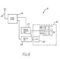
- the television receiver 31 of Figure 6 has a liquid crystal display 32 formed of a lattice of display elements 33 made from liquid crystal material, each element being individually actuable.
- the lattice of elements 33 is backlit by a number of fluorescent tubes 34 whose light intensity and duration of operation can be controlled.
- the video signal for input to television receiver has a 70Hz scan rate providing a scan period of 14mS, and includes in each picture of display information an 8-bit word for each display element, a word beginning with the most-significant-bit and ending with the least-significant-bit.
- this signal is input to receiver 31 via its aerial 35, one picture of display information passes to a frame store 36.
- frame store 36 In the processing for the display of the most-significant-bits of the word, frame store 36 outputs the first bit of each word and sends the bits to a control unit 37 for an array of drivers 38, one being assigned to each row and column of the lattice.
- the driver array sets each element to the condition (on or off) appropriate to its most-signficant-bit.
- driver control unit 37 instructs light switch unit 39 which checks the relevant bit-position (in this case the most-significant-bit) and then activates the fluorescent tubes 34 for a time duration of 3mS and at an intensity to provide an appropriate output.
- the light switch unit 39 de-activates the tubes 34 and instructs frame store 36 which proceeds to output the secondmost-significant bits to driver control unit 37 thereby to set all the elements for this bit-position.
- light switch unit 39 activates the tubes half as long as before (namely 1.5mS) at the same intensity to provide only half the output as that for the most-significant bits. This routine is repeated for all eight bits of the words, the light output being halved each time. Once the least significant bit has been displayed (the light output time duration being 25 S), the store 36 is emptied and the next picture of display information is input and the processing described above is repeated.
- Figure 7 is a block diagram of a system 40 for displaying off-air video pictures on a bistable display, such as a ferroelectric liquid crystal display panel.
- Video information is received at aerial 41 and demodulated by the receiver 42; it is then digitized (four bits per pixel) and held in the digital frame store 43.
- the data is split into four streams (one for each bit) and compressed by shift registers 44 so each byte contains data for 8 pixels.
- the data is then loaded into four buffer RAMs 45, so each RAM now contains one frame of video information 1 bit deep. Accessing of the RAMs 45 and the frame store is done under control of the address generator 46.
- the data For the sequential greyscale processing the data must be sent to the display one bit at a time, i.e. firstly all the data from RAM 0 is sent to the display (the least signficant bit), then followed in turn by each of the other 3 RAMs. Also, in order to write data to the light crystal display panel each line of data mmust be presented in a manner determined by the mulitplexing scheme; this processing is performed by the data preparation block 47. Data is now in a form in which it can be sent to the display panel under control of the multiplex controller block 48, each line of data being latched into the column drive chips 49 while rows are strobed by the row drive chips 50. This results in the data being latched into the display. After a full screen of data has been written, the backlight is flashed for a length of time corresponding to the significance of the bit being displayed. This is done by the lamp drive circuit 50 under control of the multiplex controller 48.
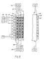
- Figure 8 shows an arrangement of metallisation patterns for a liquid crystal display panel to achieve a two-bit greyscale, for use additionally or alternatively to the greyscale processing of Figure 6 and 7.
- the ITO metallisation patterns are such that each pixel has two sections 61, 62 which can be separately driven from appropriate drive chips (not shown) on flexible pcb boards 63 and 64 via lines 65 and 66 respectively.
- section 61 corresponds to the least-significant-bit
- section 62 to the most-significant-bit.
- the row electrodes are formed by ITO metallisation strips 67 on substrate 68, which can be strobed by row drive chips (not shown) on flexible pcb 69 via lines 70.
- the substrate has been omitted as indicated by the broken-chain line yet the column metallisation is shown overlying the row metallisation, for the purpose of simplicity.
Abstract
Description
- The present invention relates to a display device incorporating liquid crystal display elements.
- British Patent Specification No. 2172733A discloses a display formed of a matrix of liquid crystal devices backlit by three light sources which are switched on sequentially each for a time duration corresponding to a third of the frame period. The intensity is controlled by using the liquid crystal elements in the variable transmission mode.
- The present invention provides a display device comprising a lattice of liquid crystal display elements, each element selectively settable between two states, one state allowing the transmission of light therethrough and the other state not allowing the transmission of light therethrough, means to effect setting of the lattice in accordance with a portion of a signal for display, and means to control the light output by the display device for a given setting of the lattice, said control means including means to render the amount of light passing through the lattice for a given setting proportional to the binary significance of that portion of the input signal.
- Preferably, the light passage means comprises means to operate, for a given setting, a light source at a light intensity proportional to the binary significance of the portion of the signal for display at that given setting.
- Advantageously, in a colour display, the light-passage means comprises means to operate three light sources of different colour characteristics, such that the intensity of each light source is proportional to the binary significance of that portion of the signal for the setting.
- The maximum intensity for the three light sources need not be the same; for example, if the three light sources are such that one emits green light, another blue light and the third red light, then the green-emitting source may have a higher maximum intensity than the red or the blue sources.
- Additionally or alternatively the light-passage means comprises means to generate a light source for a time duration proportional to the binary significance of the brightness portion of the input signal for that pixel. For a colour display, preferably the light-passage means comprises means to operate three light sources of different colour characteristics, such that the intensity of each light source is proportional to the binary significance of that colour brightness for that pixel in the input signal to the device. The maximum time duration for the three light sources need not be the same.
- Preferably, the signal for one picture comprises a sequence of words (for example each of 8 bits), each one corresponding to the display information for a display element in the lattice. Thus the output means can operate such as to take out, from the store, the first bit in each word and pass them sequentially to the lattice; thereafter the output means can operate such as to take out, from the store, the second bit in each word and pass them sequentially to the lattice. This operation can be repeated until all the bits have been processed in this way.
- As the bits in a given position (e.g. first) in the display word reach the drivers, they set each pixel to the corresponding condition. Once the entire lattice has been set in accordance with a given bit-position, the light-modulation means can be activated to output light in accordance with the given bit-position; thus, for example, if the given bit-position is the first bit in the word and this is designated as the most-significant bit, then the light output with the elements in this condition is accordingly a substantial fraction of the total output. The light for the most-significant-bit setting may be double that for the secondmost-significant-bit setting, which is itself double that for the third most-significant-bit setting, and so on. The light modulation means may have means to regulate the intensity of the light output in accordance with the given bit-position, and/or means to regulate the duration of light output in accordance with the given bit-position.
- Preferably the display device may have means to blank the elements during setting of the elements for a given bit position.
- For a colour display, preferably the display device has a lattice formed of groups of three display elements, each of the elements in a group producing a different colour and being set separately. In an alternative arrangement, the lattice is formed of single display elements, each of which is exposed to light of the three colours sequentially, an element being re-set after each exposure.
- The present invention also provide a method of operating a grey-scale display device having a lattice of bi-stable display elements, the method comprising:-
inputting a signal, representing the display information for one picture, to a store;
outputting from the store a section of the display information for one picture, the section consisting of corresponding portions of display information for all the bi-stable display elements;
using a plurality of drivers, each allocated to a row or column of the lattice, to effect setting of each display element to a condition in accordance with its respective portion of the signal from the output means;
producing a light output, once the elements are set, modulated in accordance with the significance of the portion of the video signal;
outputting from the store a second section of the display information, the second section consisting of different corresponding portions of display information for all the bi-stable display elements, and effecting the setting and modulating operations for the second section; and
repeating the outputting, setting and modulating operations on any further corresponding portions. - Preferably, the signal comprises an 8-bit word for each element, and the most-significant-bit of each word is first output from the store for setting and display. Thereafter the second-most-significant-bit of each word is output from the store for setting and display, the total light output being half the previous output. This sequence is repeated until the least-significant bit has been displayed.
- Preferably, modulation of the light output is achieved by regulation of the light intensity and/or of the duration of light output.
- Preferably, each row and column of the lattice has a separate driver. Alternatively, each column has a separate driver, and some or all the rows have a common driver.
- Preferably a display element comprises one or more selectively-settable liquid crystal cells.
- The present invention is applicable to many forms of displays, for example to one in which the image is presented at a surface of a liquid panel backlit by fluorescent tubes, or to one in which the image is projected onto a screen by means of a liquid crystal panel positioned in the path of a light beam. Also, the present invention is applicable to colour displays and to black-and-white displays.
- Furthermore, the present invention also embodies equipment for the generation, and/or transmission, and/or reception, and/or processing, of signals suited and/or designed for a display device as herein defined.
- Additionally or alternatively the light-passage means comprises means to generate a light source for a time duration proportional to the binary significance of the brightness portion of the input signal for that pixel. For a colour display, preferably the light-passage means comprises means to operate three light sources of different colour characteristics, such that the intensity of each light source is proportional to the binary significance of that colour brightness for that pixel in the input signal to the device. The maximum time duration for the three light sources need not be the same.
- In order that the invention may more readily be understood, a description is now given, by way of example only, reference being made to the accompanying drawings in which:-
- Figure 1 is a block schematic diagram of part of a display device embodying the present invention;
- Figure 2 is a diagram of waveforms for use in a display device embodying the present invention;
- Figure 3 is a diagram of waveforms for use in another embodiment of display device;
- Figure 4 is a diagram of a part of a further embodiment of the present invention;
- Figure 5 is a diagram of the sequence of waveforms in one frame for a display device embodying the present invention;
- Figure 6 is a block diagram of a display device embodying the present invention;
- Figure 7 is another block diagram of a display device embodying the present invention; and
- Figure 8 shows a pixel arrangement for a display device embodying the present invention.
- There is shown in Figure 1 part of a colour-
sequential display 1 formed by a matrix of surface-stabilised bi-stable ferroelectricliquid crystal elements 2. Eachelement 2 is separately settable, by the output of appropriate signals frommatrix driver 3 along column conductor lines 4 androw conductor lines 5, between two states, in one of which light can pass through the element and in the other of which light is prevented from passing therethrough. -
Display 1 has three sets (6, 7 and 8) of fluorescent tubes, each set providing uniform backlighting of the matrix in a respective colour (green, red, and blue) used to produce a colour display. - In order to avoid any problems of top-bottom shading, all the
elements 2 forming the matrix are set to their relevant state (i.e. light-transmitting or light-blocking) in each field before a set of fluorescent tubes is activated. - In order to provide brightness control of the display, the activation duration of the sets of fluorescent tubes is variable, being dependent on the binary significance of the brightness information for the relevant colour in the input signal. Half of the frame time (T) is used for the numerous setting operations on the matrix of elements and half is used for the backlighting operations of the various settings. The setting and backlighting operations in respect of the green light constitute half the frame time, while those for each of the red and blue light constitute quarter the frame time. This display utilises an eight bit-encoded video signal consisting of four bits dedicated to the green light information, and two bits dedicated to each of the red and blue light information.
- More specifically, in order to display the green light information in one frame, there is a sequence of four consecutive writing operations each separated by a green backlighting pulse of predetermined duration and amplitude. The writing of a stable bi-level pattern is achieved, while all the lights are off, by addressing the matrix via
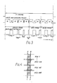
lines 4 and 5 according to the significance of the respective bit in the input video signal. For example, a bi-level pattern corresponding to the most-significant-bit is written over the entire matrix and, once completed,tube set 6 is turned on with an intensity 8Ig for a time period T/16, where Ig is a reference light intensity for the green image.Tube set 6 is then turned off for T/16, during which the matrix is overwritten to form a pattern appropriate to the next most-significant-bit, this taking T/16; once completed,tube set 6 is turned on at an intensity 4Ig for T/16. Then the light is pulsed off again for T/16, and the matrix is overwritten to produce a pattern corresponding to the next most-significant-bits for the green image, after whichtube set 6 is turned on for T/16 at intensity 2Ig. The overwriting and exposure sequence is repeated again, for a lighting intensity of Ig, whereupon display of the green image is completed. - To achieve display of the red image, a similar routine is followed but this time only two patterns are overwritten and exposed, the first pattern at an intensity of 2Ir and the second at an intensity of Ir. Each pattern is written in a time period of T/16, with tube set 7 off. For the blue image, this routine of only two patterns is repeated, at intensities 2Ib and Ib. Figure 2 shows the relevant waveforms used to produce a display with these routines.
- In an alternative form, the duration of exposure of the various patterns differs, while the intensity of the light sources remains the same for all the patterns overwritten. Thus, to display the green light information, there are four overwritten/exposure operations each having a common writing duration, but having differing exposure durations of 8tg, 4tg, 2tg and tg. Likewise each of the routines for producing the red and blue displays has two overwriting/exposure operations having differing exposure durations of 2tr and tr, or 2tb and tb respectively.
- As the
display 1 conforms to the PAL system standards, each frame must consist of 575 active lines per 40 msec which must be displayed every 20 msec to ensure a flicker-free image. In each 20 msec period, eight fields corresponding to each grey level and colour need to be written, so that the total writing time in 4.3N µsec per line, where N is the number of subdivisions of the display area that can be addressed in parallel. Such parallel addressing can be achieved in a number of ways, one of which is to utilise the arrangement of light gates and conductors as shown in Figure 4, whereby each column is made up of four sub-electrodes A, B, C and D. In this way, by doubling the number of light gates per line conductor and doubling the number of column conductors, it is possible to switch four lines simultaneously. Thus, by addressing 144 lines sequentially downwards from the top while simultaneously addressing 144 lines sequentially upwards from the bottom, a total of 576 lines are addressed in the time taken to scan 144 lines. In this instance, N = 4 and so, if all the fields are to be written in 20ms, the time available for writing is 17 µsec per line. - In a modification, both the duration of exposure and the intensity of the light sources can be made to be variable.
- The three
sets 6, 7, 8 of fluorescent tubes are contained in a housing designed to provide a uniform flux of each colour into the display. The sets of tubes used in the backlight are low pressure mercury/rare gas (LPMV) discharge lamps coated on the inside wall with a phosphor, chosen to have appropriate spectral distribution, rise and decay time characteristics. The lamps are run off a high frequency supply ( >10 kHz) which is switched sequentially between the three lamps using non-rectifying thyristor switching elements. The on-time of the lamp may be made variable, consistent with the transmissive mode window of the display to provide colour balance and overall brightness adjustment. - Figure 5 shows a sequence of addressing signals appropriate to produce an 8-colour display suitable for most alphagraphics and capable of three times the resolution of a microdot colour display, since it requires only one cell per picture element. With a suitable liquid crystal display device it would be possible to arrange for temporal and/or spatial modulation of each gate to provide halftoning.
- The use of a bi-stable ferroelectric liquid crystal display in the manner described above enables the possibility of providing for each pixel, six colours together with black and white.
- The colour-sequential technique of addressing mentioned above requires the tubes to run at frequencies greater than about 65 Hz in order to provide flicker-free displays. There is about 5 msec available for each frame of information on an individual colour, during which period the information has to be written on the display and illuminated. Such time restraints require the phosphor to be used to have specific characteristics including a narrow band emission at an appropriate wavelength and a decay time (i.e. time to fall to 10% of maximum or operational output) of less than 1 msec. Cheap wide band (light transmission) filters are used to filter out the mercury spectral lines from the light output.
- Resistive ballasts are used if square light pulses are required to illuminate the display, and also because they do not introduce any delays into the circuit. By making part of the ballast resistance variable, the overall screen brightness and colour can be simply adjusted. The pulse shape of the light output can be altered by appropriate choice of ballast components, for example, using reactive components. The possibility of shaping the light output pulses allows the lines of display to be switched whilst the lamps are on.
- The sequence of illuminating the sets of tubes can be important to the overall performance, and image-quality, of the display. Thus for example the illuminations sequence of red light sources, then green light sources, then blue light sources can substantially affect the colour performance as compared to the sequence of red, then blue, then green sources.
- The colour of the 6 available colours of the display can be altered by changing the phase of the lamp pulse with respect to the LCD drivers. In effect, this moves a window across the light output.
- The colour of each individual pixel can be adjusted to give more than the 6 colours previously mentioned by a similar technique to that used to give control of the brightness of each individual pixel (greyscale).
- The
television receiver 31 of Figure 6 has aliquid crystal display 32 formed of a lattice ofdisplay elements 33 made from liquid crystal material, each element being individually actuable. The lattice ofelements 33 is backlit by a number offluorescent tubes 34 whose light intensity and duration of operation can be controlled. - The video signal for input to television receiver has a 70Hz scan rate providing a scan period of 14mS, and includes in each picture of display information an 8-bit word for each display element, a word beginning with the most-significant-bit and ending with the least-significant-bit. When this signal is input to
receiver 31 via its aerial 35, one picture of display information passes to aframe store 36. - In the processing for the display of the most-significant-bits of the word,
frame store 36 outputs the first bit of each word and sends the bits to acontrol unit 37 for an array ofdrivers 38, one being assigned to each row and column of the lattice. The driver array sets each element to the condition (on or off) appropriate to its most-signficant-bit. Once the array ofdrivers 38 has set all the elements (which takes less than 1mS),driver control unit 37 instructslight switch unit 39 which checks the relevant bit-position (in this case the most-significant-bit) and then activates thefluorescent tubes 34 for a time duration of 3mS and at an intensity to provide an appropriate output. - When the required output has been achieved then the
light switch unit 39 de-activates thetubes 34 and instructsframe store 36 which proceeds to output the secondmost-significant bits todriver control unit 37 thereby to set all the elements for this bit-position. On this occasion,light switch unit 39 activates the tubes half as long as before (namely 1.5mS) at the same intensity to provide only half the output as that for the most-significant bits. This routine is repeated for all eight bits of the words, the light output being halved each time. Once the least significant bit has been displayed (the light output time duration being 25 S), thestore 36 is emptied and the next picture of display information is input and the processing described above is repeated. - Figure 7 is a block diagram of a
system 40 for displaying off-air video pictures on a bistable display, such as a ferroelectric liquid crystal display panel. Video information is received at aerial 41 and demodulated by thereceiver 42; it is then digitized (four bits per pixel) and held in thedigital frame store 43. - To display one video frame, firstly the data is split into four streams (one for each bit) and compressed by
shift registers 44 so each byte contains data for 8 pixels. The data is then loaded into fourbuffer RAMs 45, so each RAM now contains one frame ofvideo information 1 bit deep. Accessing of theRAMs 45 and the frame store is done under control of theaddress generator 46. - For the sequential greyscale processing the data must be sent to the display one bit at a time, i.e. firstly all the data from RAM 0 is sent to the display (the least signficant bit), then followed in turn by each of the other 3 RAMs. Also, in order to write data to the light crystal display panel each line of data mmust be presented in a manner determined by the mulitplexing scheme; this processing is performed by the
data preparation block 47. Data is now in a form in which it can be sent to the display panel under control of themultiplex controller block 48, each line of data being latched into the column drive chips 49 while rows are strobed by the row drive chips 50. This results in the data being latched into the display. After a full screen of data has been written, the backlight is flashed for a length of time corresponding to the significance of the bit being displayed. This is done by thelamp drive circuit 50 under control of themultiplex controller 48. - The sequence of events which results in a full picture with sixteen grey levels being displayed, is as follows:-
- 1.
Load frame store 43; - 2. Load buffer RAMs 45, one significant bit to each;
- 3. Load data from buffer RAM 0 line by line into
data preparation unit 47; - 4. Load data from
buffer RAM 1 line by line intodata preparation unit 47; - 5. Load data from
buffer RAM 2 line by line intodata preparation unit 47; - 6. Load data from
buffer RAM 3 line by line intodata preparation unit 47; - 7.
Multiplex controller 48 sends data frompreparation unit 47 to column drive chips 49 and controls row drive chips 50; - 8. When data from RAM 0 has been latched into the display (i.e. when the least significant bit for the frame is being presented), the
multiplex controller 49 signals the lamp drive to flash for a period of time A mS; - 9. Data from
RAM 1 is now latched and the backlight flashed for 2A mS; - 10. Data from
RAM 2 is now latched and the backlight flashed for 4A mS; - 11. Data from
RAM 3 is now latched and the backlight flashed for 8A mS; - 12. The picture has now been displayed.
- Figure 8 shows an arrangement of metallisation patterns for a liquid crystal display panel to achieve a two-bit greyscale, for use additionally or alternatively to the greyscale processing of Figure 6 and 7. On the susbtrate 30 having the column electrodes, the ITO metallisation patterns are such that each pixel has two
sections flexible pcb boards lines section 61 corresponds to the least-significant-bit, andsection 62 to the most-significant-bit. The row electrodes are formed by ITO metallisation strips 67 onsubstrate 68, which can be strobed by row drive chips (not shown) on flexible pcb 69 vialines 70. In Figure 8, on the left hand side the substrate has been omitted as indicated by the broken-chain line yet the column metallisation is shown overlying the row metallisation, for the purpose of simplicity.
Claims (10)
Priority Applications (1)
| Application Number | Priority Date | Filing Date | Title |
|---|---|---|---|
| AT87308309T ATE89426T1 (en) | 1986-09-20 | 1987-09-18 | INDICATOR. |
Applications Claiming Priority (4)
| Application Number | Priority Date | Filing Date | Title |
|---|---|---|---|
| GB8622711 | 1986-09-20 | ||
| GB868622711A GB8622711D0 (en) | 1986-09-20 | 1986-09-20 | Display device |
| GB878716162A GB8716162D0 (en) | 1987-07-09 | 1987-07-09 | Display device |
| GB8716162 | 1987-07-09 |
Publications (3)
| Publication Number | Publication Date |
|---|---|
| EP0261896A2 true EP0261896A2 (en) | 1988-03-30 |
| EP0261896A3 EP0261896A3 (en) | 1989-01-11 |
| EP0261896B1 EP0261896B1 (en) | 1993-05-12 |
Family
ID=26291316
Family Applications (1)
| Application Number | Title | Priority Date | Filing Date |
|---|---|---|---|
| EP87308309A Expired - Lifetime EP0261896B1 (en) | 1986-09-20 | 1987-09-18 | Display device |
Country Status (6)
| Country | Link |
|---|---|
| US (1) | US5122791A (en) |
| EP (1) | EP0261896B1 (en) |
| JP (1) | JP2567871B2 (en) |
| CA (1) | CA1294720C (en) |
| DE (1) | DE3785813T2 (en) |
| ES (1) | ES2040258T3 (en) |
Cited By (24)
| Publication number | Priority date | Publication date | Assignee | Title |
|---|---|---|---|---|
| EP0342835A1 (en) * | 1988-05-18 | 1989-11-23 | Stc Plc | Liquid crystal cell addressing |
| GB2235847A (en) * | 1989-07-05 | 1991-03-13 | Gold Star Co | Automatic backlight on/off for liquid crystal display television |
| FR2662271A1 (en) * | 1990-05-18 | 1991-11-22 | Thomson Lcd | Optical system for reproducing video images |
| US5170100A (en) * | 1990-03-06 | 1992-12-08 | Hangzhou University | Electronic fluorescent display system |
| US5233338A (en) * | 1990-09-25 | 1993-08-03 | Thorn Emi Plc | Display devices having color sequential illumination |
| WO1994009473A1 (en) * | 1992-10-15 | 1994-04-28 | Rank Brimar Limited | Display device |
| WO1994010675A1 (en) * | 1992-11-04 | 1994-05-11 | Rank Brimar Limited | Display system |
| WO1995001701A1 (en) * | 1993-06-30 | 1995-01-12 | Philips Electronics N.V. | Matrix display systems and methods of operating such systems |
| US5402143A (en) * | 1991-12-23 | 1995-03-28 | Panocorp Display Systems | Color fluorescent liquid crystal display |
| WO1995011572A1 (en) * | 1993-10-21 | 1995-04-27 | Philips Electronics N.V. | Image projection device and lamp control system for use therein |
| EP0660593A1 (en) * | 1993-12-24 | 1995-06-28 | Sony Corporation | Method for displaying gradations |
| EP0662773A1 (en) * | 1994-01-07 | 1995-07-12 | Texas Instruments Incorporated | Method and apparatus for sequential color imaging |
| WO1995027970A1 (en) * | 1994-04-12 | 1995-10-19 | Rank Brimar Limited | Display device |
| US5565742A (en) * | 1991-02-25 | 1996-10-15 | Panocorp Display Systems | Electronic fluorescent display |
| NL1001925C2 (en) * | 1994-12-21 | 1997-05-02 | Hughes Aircraft Co | Image projection system. |
| EP0709823A3 (en) * | 1994-10-24 | 1997-10-22 | Aoki Kazuo | Panel type color display device and system for processing image information |
| EP0889458A2 (en) | 1997-07-02 | 1999-01-07 | Sony Corporation | Method and device for driving a spatial light modulator |
| US6377002B1 (en) | 1994-09-15 | 2002-04-23 | Pixtech, Inc. | Cold cathode field emitter flat screen display |
| EP1532481A2 (en) * | 2002-05-06 | 2005-05-25 | Uni-Pixel Displays, Inc. | Field sequential color efficiency |
| WO2007040732A1 (en) * | 2005-09-14 | 2007-04-12 | Hewlett-Packard Development Company, L.P. | Image display system and method |
| WO2007042267A3 (en) * | 2005-10-11 | 2007-07-12 | Barco Nv | Display assemblies and methods of display |
| US7253794B2 (en) | 1995-01-31 | 2007-08-07 | Acacia Patent Acquisition Corporation | Display apparatus and method |
| WO2007096805A1 (en) * | 2006-02-22 | 2007-08-30 | Philips Intellectual Property & Standards Gmbh | Method of colour image projection using spatial light modulation and light source modulation |
| EP2360668A1 (en) * | 2010-01-15 | 2011-08-24 | Samsung Electronics Co., Ltd. | Backlight unit and display apparatus |
Families Citing this family (85)
| Publication number | Priority date | Publication date | Assignee | Title |
|---|---|---|---|---|
| JPH0827453B2 (en) * | 1986-09-29 | 1996-03-21 | セイコー電子工業株式会社 | Ferroelectric liquid crystal color electro-optical device |
| JP2608431B2 (en) * | 1987-12-16 | 1997-05-07 | スタンレー電気株式会社 | Liquid crystal display device |
| JP2734570B2 (en) * | 1988-11-08 | 1998-03-30 | ヤマハ株式会社 | Liquid crystal display circuit |
| KR100202246B1 (en) * | 1989-02-27 | 1999-06-15 | 윌리엄 비. 켐플러 | Apparatus and method for digital video system |
| US6535187B1 (en) | 1998-04-21 | 2003-03-18 | Lawson A. Wood | Method for using a spatial light modulator |
| US5416496A (en) * | 1989-08-22 | 1995-05-16 | Wood; Lawson A. | Ferroelectric liquid crystal display apparatus and method |
| US6348907B1 (en) | 1989-08-22 | 2002-02-19 | Lawson A. Wood | Display apparatus with digital micromirror device |
| KR940004138B1 (en) * | 1990-04-06 | 1994-05-13 | Canon Kk | Display apparatus |
| TW228633B (en) * | 1991-01-17 | 1994-08-21 | Semiconductor Energy Res Co Ltd | |
| JPH0743738A (en) * | 1991-01-17 | 1995-02-14 | Semiconductor Energy Lab Co Ltd | Liquid crystal electro-optical device |
| JP2704581B2 (en) * | 1991-11-20 | 1998-01-26 | 株式会社半導体エネルギー研究所 | Image display device |
| US5428366A (en) * | 1992-09-09 | 1995-06-27 | Dimension Technologies, Inc. | Field sequential color illumination system for liquid crystal display |
| JPH10503030A (en) * | 1993-11-28 | 1998-03-17 | スマートライト・リミテッド | Fluoroscopy device with passive matrix LCD |
| JP3145552B2 (en) * | 1993-12-28 | 2001-03-12 | セイコーインスツルメンツ株式会社 | Liquid crystal display panel drive device |
| JP3027298B2 (en) * | 1994-05-31 | 2000-03-27 | シャープ株式会社 | Liquid crystal display with backlight control function |
| US6184969B1 (en) * | 1994-10-25 | 2001-02-06 | James L. Fergason | Optical display system and method, active and passive dithering using birefringence, color image superpositioning and display enhancement |
| US5715029A (en) * | 1994-10-25 | 1998-02-03 | Fergason; James L. | Optical dithering system using birefringence for optical displays and method |
| US5757348A (en) * | 1994-12-22 | 1998-05-26 | Displaytech, Inc. | Active matrix liquid crystal image generator with hybrid writing scheme |
| US5748164A (en) * | 1994-12-22 | 1998-05-05 | Displaytech, Inc. | Active matrix liquid crystal image generator |
| US5808800A (en) | 1994-12-22 | 1998-09-15 | Displaytech, Inc. | Optics arrangements including light source arrangements for an active matrix liquid crystal image generator |
| JP3062418B2 (en) * | 1995-06-02 | 2000-07-10 | キヤノン株式会社 | Display device, display system, and display control method |
| US5767828A (en) * | 1995-07-20 | 1998-06-16 | The Regents Of The University Of Colorado | Method and apparatus for displaying grey-scale or color images from binary images |
| US5959598A (en) | 1995-07-20 | 1999-09-28 | The Regents Of The University Of Colorado | Pixel buffer circuits for implementing improved methods of displaying grey-scale or color images |
| JP3215913B2 (en) * | 1997-07-30 | 2001-10-09 | 富士通株式会社 | Display control method of liquid crystal display device and liquid crystal display device |
| US6232963B1 (en) * | 1997-09-30 | 2001-05-15 | Texas Instruments Incorporated | Modulated-amplitude illumination for spatial light modulator |
| WO1999023456A1 (en) | 1997-10-30 | 1999-05-14 | Baker Electronics, Inc. | Consistent brightness backlight system |
| JP3049061B1 (en) * | 1999-02-26 | 2000-06-05 | キヤノン株式会社 | Image display device and image display method |
| JP3971026B2 (en) * | 1998-06-22 | 2007-09-05 | シチズンホールディングス株式会社 | Liquid crystal display |
| US6809717B2 (en) * | 1998-06-24 | 2004-10-26 | Canon Kabushiki Kaisha | Display apparatus, liquid crystal display apparatus and driving method for display apparatus |
| JP2000241796A (en) * | 1998-12-24 | 2000-09-08 | Sharp Corp | Liquid crystal display device and electronic equipment outputting control signal of liquid crystal display device |
| JP2000214825A (en) * | 1999-01-20 | 2000-08-04 | Nec Corp | Backlight display device and method |
| JP2000275604A (en) * | 1999-03-23 | 2000-10-06 | Hitachi Ltd | Liquid crystal display device |
| KR20010050623A (en) * | 1999-10-04 | 2001-06-15 | 모리시타 요이찌 | Display technique for high gradation degree |
| KR100327375B1 (en) * | 2000-03-06 | 2002-03-06 | 구자홍 | apparatus for active driver |
| KR100385880B1 (en) * | 2000-12-15 | 2003-06-02 | 엘지.필립스 엘시디 주식회사 | Method of Driving Liquid Crystal Display |
| WO2002056288A1 (en) * | 2001-01-10 | 2002-07-18 | Mitsubishi Denki Kabushiki Kaisha | Color image display |
| JP3471782B2 (en) * | 2001-02-13 | 2003-12-02 | Nec液晶テクノロジー株式会社 | Flat fluorescent lamp unit and liquid crystal display device using the same |
| EP2312380B1 (en) | 2001-02-27 | 2020-11-18 | Dolby Laboratories Licensing Corporation | A method and device for displaying an image |
| EP1390941A1 (en) * | 2001-04-18 | 2004-02-25 | Kent Displays Incorporated | Active matrix addressed bistable reflective cholesteric displays and graphic controllers and operating methods therefor |
| JP3850241B2 (en) * | 2001-07-19 | 2006-11-29 | シャープ株式会社 | LIGHTING DEVICE AND LIQUID CRYSTAL DISPLAY DEVICE USING THE SAME |
| JP3840940B2 (en) * | 2001-09-28 | 2006-11-01 | 株式会社日立製作所 | Image display device |
| US7064740B2 (en) * | 2001-11-09 | 2006-06-20 | Sharp Laboratories Of America, Inc. | Backlit display with improved dynamic range |
| KR100673666B1 (en) * | 2002-02-26 | 2007-01-24 | 유니-픽셀 디스플레이스, 인코포레이티드 | Enhancements to optical flat panel displays |
| US8687271B2 (en) | 2002-03-13 | 2014-04-01 | Dolby Laboratories Licensing Corporation | N-modulation displays and related methods |
| JP4348457B2 (en) * | 2002-03-13 | 2009-10-21 | ドルビー ラボラトリーズ ライセンシング コーポレイション | High dynamic range display, display controller, and image display method |
| US20030184506A1 (en) * | 2002-04-02 | 2003-10-02 | Koninklijke Philips Electronics N.V. | Current modulation method for liquid crystal display projection lamp |
| JP4169589B2 (en) * | 2002-12-13 | 2008-10-22 | 富士通株式会社 | Display device and display method |
| US8243004B2 (en) * | 2003-03-10 | 2012-08-14 | Fergason Patent Properties, Llc | Apparatus and method for preparing, storing, transmitting and displaying images |
| US7623105B2 (en) | 2003-11-21 | 2009-11-24 | Sharp Laboratories Of America, Inc. | Liquid crystal display with adaptive color |
| KR20050053447A (en) * | 2003-12-02 | 2005-06-08 | 엘지.필립스 엘시디 주식회사 | Liquid crystal display device and the method thereof |
| KR100875326B1 (en) * | 2003-12-18 | 2008-12-22 | 샤프 가부시키가이샤 | Liquid crystal display response characteristics determination method and presentation method |
| US8395577B2 (en) | 2004-05-04 | 2013-03-12 | Sharp Laboratories Of America, Inc. | Liquid crystal display with illumination control |
| US20050248553A1 (en) * | 2004-05-04 | 2005-11-10 | Sharp Laboratories Of America, Inc. | Adaptive flicker and motion blur control |
| US7872631B2 (en) | 2004-05-04 | 2011-01-18 | Sharp Laboratories Of America, Inc. | Liquid crystal display with temporal black point |
| US7612757B2 (en) | 2004-05-04 | 2009-11-03 | Sharp Laboratories Of America, Inc. | Liquid crystal display with modulated black point |
| US7777714B2 (en) | 2004-05-04 | 2010-08-17 | Sharp Laboratories Of America, Inc. | Liquid crystal display with adaptive width |
| US7532192B2 (en) | 2004-05-04 | 2009-05-12 | Sharp Laboratories Of America, Inc. | Liquid crystal display with filtered black point |
| US7505018B2 (en) * | 2004-05-04 | 2009-03-17 | Sharp Laboratories Of America, Inc. | Liquid crystal display with reduced black level insertion |
| US7023451B2 (en) * | 2004-06-14 | 2006-04-04 | Sharp Laboratories Of America, Inc. | System for reducing crosstalk |
| US7556836B2 (en) | 2004-09-03 | 2009-07-07 | Solae, Llc | High protein snack product |
| US7898519B2 (en) * | 2005-02-17 | 2011-03-01 | Sharp Laboratories Of America, Inc. | Method for overdriving a backlit display |
| EP1650736A1 (en) * | 2004-10-25 | 2006-04-26 | Barco NV | Backlight modulation for display |
| US7525528B2 (en) | 2004-11-16 | 2009-04-28 | Sharp Laboratories Of America, Inc. | Technique that preserves specular highlights |
| US8050511B2 (en) | 2004-11-16 | 2011-11-01 | Sharp Laboratories Of America, Inc. | High dynamic range images from low dynamic range images |
| US8050512B2 (en) | 2004-11-16 | 2011-11-01 | Sharp Laboratories Of America, Inc. | High dynamic range images from low dynamic range images |
| TW200705005A (en) * | 2005-07-22 | 2007-02-01 | Ind Tech Res Inst | Liquid crystal display |
| WO2007016511A2 (en) * | 2005-08-02 | 2007-02-08 | Uni-Pixel Displays, Inc. | Mechanism to mitigate color breakup artifacts in field sequential color display systems |
| US20070063996A1 (en) * | 2005-09-14 | 2007-03-22 | Childers Winthrop D | Image display system and method |
| US20070064008A1 (en) * | 2005-09-14 | 2007-03-22 | Childers Winthrop D | Image display system and method |
| US7551154B2 (en) | 2005-09-15 | 2009-06-23 | Hewlett-Packard Development Company, L.P. | Image display system and method |
| US9143657B2 (en) | 2006-01-24 | 2015-09-22 | Sharp Laboratories Of America, Inc. | Color enhancement technique using skin color detection |
| US8121401B2 (en) | 2006-01-24 | 2012-02-21 | Sharp Labortories of America, Inc. | Method for reducing enhancement of artifacts and noise in image color enhancement |
| JP4645486B2 (en) * | 2006-03-13 | 2011-03-09 | セイコーエプソン株式会社 | Image display device and projector |
| US8941580B2 (en) | 2006-11-30 | 2015-01-27 | Sharp Laboratories Of America, Inc. | Liquid crystal display with area adaptive backlight |
| US8471807B2 (en) * | 2007-02-01 | 2013-06-25 | Dolby Laboratories Licensing Corporation | Calibration of displays having spatially-variable backlight |
| US8203547B2 (en) * | 2007-06-15 | 2012-06-19 | Ricoh Co. Ltd | Video playback on electronic paper displays |
| US8355018B2 (en) * | 2007-06-15 | 2013-01-15 | Ricoh Co., Ltd. | Independent pixel waveforms for updating electronic paper displays |
| US8416197B2 (en) * | 2007-06-15 | 2013-04-09 | Ricoh Co., Ltd | Pen tracking and low latency display updates on electronic paper displays |
| US8319766B2 (en) * | 2007-06-15 | 2012-11-27 | Ricoh Co., Ltd. | Spatially masked update for electronic paper displays |
| US8913000B2 (en) * | 2007-06-15 | 2014-12-16 | Ricoh Co., Ltd. | Video playback on electronic paper displays |
| US8279232B2 (en) * | 2007-06-15 | 2012-10-02 | Ricoh Co., Ltd. | Full framebuffer for electronic paper displays |
| US20090322800A1 (en) | 2008-06-25 | 2009-12-31 | Dolby Laboratories Licensing Corporation | Method and apparatus in various embodiments for hdr implementation in display devices |
| CN101719352B (en) | 2008-10-09 | 2012-07-25 | 北京京东方光电科技有限公司 | Device and method for detection after forming liquid crystal box |
| US20100214282A1 (en) | 2009-02-24 | 2010-08-26 | Dolby Laboratories Licensing Corporation | Apparatus for providing light source modulation in dual modulator displays |
| WO2012124623A1 (en) * | 2011-03-17 | 2012-09-20 | シャープ株式会社 | Liquid crystal display device and method for driving same |
Citations (8)
| Publication number | Priority date | Publication date | Assignee | Title |
|---|---|---|---|---|
| US4090219A (en) * | 1974-12-09 | 1978-05-16 | Hughes Aircraft Company | Liquid crystal sequential color display |
| US4378568A (en) * | 1981-01-29 | 1983-03-29 | Eastman Kodak Company | Light valve imaging apparatus and method for providing gray scale |
| US4380023A (en) * | 1981-01-29 | 1983-04-12 | Eastman Kodak Company | Electronic imaging apparatus with light valve area arrays |
| JPS6089042A (en) * | 1983-10-21 | 1985-05-18 | Toshiba Corp | Color display device |
| JPS60163023A (en) * | 1984-02-03 | 1985-08-24 | Seiko Epson Corp | Liquid crystal display body |
| JPS60260922A (en) * | 1984-06-07 | 1985-12-24 | Citizen Watch Co Ltd | Display lighting device for liquid crystal element |
| EP0174497A2 (en) * | 1984-08-29 | 1986-03-19 | Hitachi, Ltd. | Electronic instrument panel |
| GB2172733A (en) * | 1985-03-05 | 1986-09-24 | Lohja Ab Oy | Colour displays |
Family Cites Families (15)
| Publication number | Priority date | Publication date | Assignee | Title |
|---|---|---|---|---|
| US3590156A (en) * | 1968-08-28 | 1971-06-29 | Zenith Radio Corp | Flat panel display system with time-modulated gray scale |
| GB1390925A (en) * | 1971-09-01 | 1975-04-16 | Rank Organisation Ltd | Optical display device |
| US3845243A (en) * | 1973-02-28 | 1974-10-29 | Owens Illinois Inc | System for producing a gray scale with a gaseous display and storage panel using multiple discharge elements |
| US4006298A (en) * | 1975-05-20 | 1977-02-01 | Gte Laboratories Incorporated | Bistable matrix television display system |
| JPS54109722A (en) * | 1978-02-16 | 1979-08-28 | Sony Corp | Flat-type picture display device |
| US4368826A (en) * | 1979-05-21 | 1983-01-18 | Thompson Mortimer S | Bottles with attached handles and a method of forming the same |
| JPS57130887U (en) * | 1981-02-10 | 1982-08-14 | ||
| US4559535A (en) * | 1982-07-12 | 1985-12-17 | Sigmatron Nova, Inc. | System for displaying information with multiple shades of a color on a thin-film EL matrix display panel |
| JPS6037591A (en) * | 1983-08-11 | 1985-02-26 | 日本電気株式会社 | Color display and driving thereof |
| GB8402654D0 (en) * | 1984-02-01 | 1984-03-07 | Secr Defence | Flatpanel display |
| DE3466817D1 (en) * | 1984-02-15 | 1987-11-19 | Ibm | Colour display apparatus and method of coding a colour image |
| JPS6126027A (en) * | 1984-07-17 | 1986-02-05 | Seiko Epson Corp | Driving circuit of liquid crystal display panel |
| US4709995A (en) * | 1984-08-18 | 1987-12-01 | Canon Kabushiki Kaisha | Ferroelectric display panel and driving method therefor to achieve gray scale |
| DE3686428T2 (en) * | 1985-03-08 | 1993-01-14 | Ascii Corp | DISPLAY CONTROL SYSTEM. |
| US4720706A (en) * | 1985-08-26 | 1988-01-19 | Stine Edward V | Method and apparatus for electro-optical color imaging |
-
1987
- 1987-09-18 DE DE87308309T patent/DE3785813T2/en not_active Expired - Lifetime
- 1987-09-18 ES ES198787308309T patent/ES2040258T3/en not_active Expired - Lifetime
- 1987-09-18 EP EP87308309A patent/EP0261896B1/en not_active Expired - Lifetime
- 1987-09-21 CA CA000547371A patent/CA1294720C/en not_active Expired - Lifetime
- 1987-09-21 JP JP62235071A patent/JP2567871B2/en not_active Expired - Lifetime
- 1987-09-21 US US07/099,376 patent/US5122791A/en not_active Expired - Lifetime
Patent Citations (8)
| Publication number | Priority date | Publication date | Assignee | Title |
|---|---|---|---|---|
| US4090219A (en) * | 1974-12-09 | 1978-05-16 | Hughes Aircraft Company | Liquid crystal sequential color display |
| US4378568A (en) * | 1981-01-29 | 1983-03-29 | Eastman Kodak Company | Light valve imaging apparatus and method for providing gray scale |
| US4380023A (en) * | 1981-01-29 | 1983-04-12 | Eastman Kodak Company | Electronic imaging apparatus with light valve area arrays |
| JPS6089042A (en) * | 1983-10-21 | 1985-05-18 | Toshiba Corp | Color display device |
| JPS60163023A (en) * | 1984-02-03 | 1985-08-24 | Seiko Epson Corp | Liquid crystal display body |
| JPS60260922A (en) * | 1984-06-07 | 1985-12-24 | Citizen Watch Co Ltd | Display lighting device for liquid crystal element |
| EP0174497A2 (en) * | 1984-08-29 | 1986-03-19 | Hitachi, Ltd. | Electronic instrument panel |
| GB2172733A (en) * | 1985-03-05 | 1986-09-24 | Lohja Ab Oy | Colour displays |
Non-Patent Citations (3)
| Title |
|---|
| PATENT ABSTRACTS OF JAPAN, vol. 10, no. 140 (P-458)(2197), 23rd May 1986; & JP - A - 60 260 922 (CITIZEN TOKEI) 24-12-1985 * |
| PATENT ABSTRACTS OF JAPAN, vol. 10, no. 7 (P-419)(2064), 11th january 1986; & JP - A - 60 163 023 (SUWA SEIKOSHA) 24-08-1985 * |
| PATENT ABSTRACTS OF JAPAN, vol. 9, no. 234 (E-344)(1957), 20th September 1985; & JP - A - 60 889 042 (TOSHIBA) 08-05-1985 * |
Cited By (39)
| Publication number | Priority date | Publication date | Assignee | Title |
|---|---|---|---|---|
| EP0342835A1 (en) * | 1988-05-18 | 1989-11-23 | Stc Plc | Liquid crystal cell addressing |
| GB2235847A (en) * | 1989-07-05 | 1991-03-13 | Gold Star Co | Automatic backlight on/off for liquid crystal display television |
| GB2235847B (en) * | 1989-07-05 | 1993-07-21 | Gold Star Co | Automatic backlight on/off control apparatus for liquid crystal display television |
| US5170100A (en) * | 1990-03-06 | 1992-12-08 | Hangzhou University | Electronic fluorescent display system |
| US5621284A (en) * | 1990-03-06 | 1997-04-15 | Pixtech, Inc. | Electronic fluorescent display system |
| FR2662271A1 (en) * | 1990-05-18 | 1991-11-22 | Thomson Lcd | Optical system for reproducing video images |
| US5233338A (en) * | 1990-09-25 | 1993-08-03 | Thorn Emi Plc | Display devices having color sequential illumination |
| US5565742A (en) * | 1991-02-25 | 1996-10-15 | Panocorp Display Systems | Electronic fluorescent display |
| US5402143A (en) * | 1991-12-23 | 1995-03-28 | Panocorp Display Systems | Color fluorescent liquid crystal display |
| WO1994009473A1 (en) * | 1992-10-15 | 1994-04-28 | Rank Brimar Limited | Display device |
| US5986640A (en) * | 1992-10-15 | 1999-11-16 | Digital Projection Limited | Display device using time division modulation to display grey scale |
| WO1994010675A1 (en) * | 1992-11-04 | 1994-05-11 | Rank Brimar Limited | Display system |
| US5912651A (en) * | 1993-06-30 | 1999-06-15 | U.S. Philips Corporation | Matrix display systems and methods of operating such systems |
| WO1995001701A1 (en) * | 1993-06-30 | 1995-01-12 | Philips Electronics N.V. | Matrix display systems and methods of operating such systems |
| WO1995011572A1 (en) * | 1993-10-21 | 1995-04-27 | Philips Electronics N.V. | Image projection device and lamp control system for use therein |
| US5917558A (en) * | 1993-10-21 | 1999-06-29 | Philips Electronics North America Corp. | Method for controlling a color projection video system |
| EP0660593A1 (en) * | 1993-12-24 | 1995-06-28 | Sony Corporation | Method for displaying gradations |
| EP0662773A1 (en) * | 1994-01-07 | 1995-07-12 | Texas Instruments Incorporated | Method and apparatus for sequential color imaging |
| WO1995027970A1 (en) * | 1994-04-12 | 1995-10-19 | Rank Brimar Limited | Display device |
| US6377002B1 (en) | 1994-09-15 | 2002-04-23 | Pixtech, Inc. | Cold cathode field emitter flat screen display |
| EP0709823A3 (en) * | 1994-10-24 | 1997-10-22 | Aoki Kazuo | Panel type color display device and system for processing image information |
| NL1001925C2 (en) * | 1994-12-21 | 1997-05-02 | Hughes Aircraft Co | Image projection system. |
| US5903323A (en) * | 1994-12-21 | 1999-05-11 | Raytheon Company | Full color sequential image projection system incorporating time modulated illumination |
| US7782280B2 (en) | 1995-01-31 | 2010-08-24 | Acacia Patent Acquisition Corporation | Display apparatus and method |
| US7253794B2 (en) | 1995-01-31 | 2007-08-07 | Acacia Patent Acquisition Corporation | Display apparatus and method |
| EP0889458A2 (en) | 1997-07-02 | 1999-01-07 | Sony Corporation | Method and device for driving a spatial light modulator |
| US6008929A (en) * | 1997-07-02 | 1999-12-28 | Sony Corporation | Image displaying apparatus and method |
| EP0889458A3 (en) * | 1997-07-02 | 1999-03-31 | Sony Corporation | Method and device for driving a spatial light modulator |
| KR100865325B1 (en) * | 1997-07-02 | 2009-02-05 | 소니 가부시끼 가이샤 | Image display device and image display method |
| EP1532481A4 (en) * | 2002-05-06 | 2009-04-22 | Uni Pixel Displays Inc | Field sequential color efficiency |
| EP1532481A2 (en) * | 2002-05-06 | 2005-05-25 | Uni-Pixel Displays, Inc. | Field sequential color efficiency |
| WO2007040732A1 (en) * | 2005-09-14 | 2007-04-12 | Hewlett-Packard Development Company, L.P. | Image display system and method |
| WO2007042267A3 (en) * | 2005-10-11 | 2007-07-12 | Barco Nv | Display assemblies and methods of display |
| US8400607B2 (en) | 2005-10-11 | 2013-03-19 | Barco N.V. | Display assemblies and methods of display |
| EP2843465A1 (en) * | 2005-10-11 | 2015-03-04 | Barco NV | Display assemblies and methods of display |
| WO2007096805A1 (en) * | 2006-02-22 | 2007-08-30 | Philips Intellectual Property & Standards Gmbh | Method of colour image projection using spatial light modulation and light source modulation |
| KR101333030B1 (en) * | 2006-02-22 | 2013-11-26 | 코닌클리케 필립스 엔.브이. | Method of colour image projection using spatial light modulation and light source modulation |
| EP2360668A1 (en) * | 2010-01-15 | 2011-08-24 | Samsung Electronics Co., Ltd. | Backlight unit and display apparatus |
| US9125276B2 (en) | 2010-01-15 | 2015-09-01 | Samsung Electronics Co., Ltd. | Backlight unit including first and second driving currents and display apparatus using the same |
Also Published As
| Publication number | Publication date |
|---|---|
| ES2040258T3 (en) | 1993-10-16 |
| EP0261896A3 (en) | 1989-01-11 |
| EP0261896B1 (en) | 1993-05-12 |
| DE3785813D1 (en) | 1993-06-17 |
| US5122791A (en) | 1992-06-16 |
| JP2567871B2 (en) | 1996-12-25 |
| JPS63113426A (en) | 1988-05-18 |
| DE3785813T2 (en) | 1993-11-11 |
| CA1294720C (en) | 1992-01-21 |
Similar Documents
| Publication | Publication Date | Title |
|---|---|---|
| EP0261896B1 (en) | Display device | |
| US5731794A (en) | Color panel display device | |
| JP3266288B2 (en) | Display device and operation method thereof | |
| US4843381A (en) | Field sequential color liquid crystal display and method | |
| US5093652A (en) | Display device | |
| US5912651A (en) | Matrix display systems and methods of operating such systems | |
| US6239780B1 (en) | Multiplexed display element sequential color LCD panel | |
| US6243072B1 (en) | Method or apparatus for displaying greyscale or color images from binary images | |
| US6831621B2 (en) | Liquid crystal display device | |
| JP2003280600A (en) | Display device, and its driving method | |
| US20090251401A1 (en) | Display Utilizing Simultaneous Color Intelligent Backlighting and luminescence Controlling Shutters | |
| IL145590A (en) | Fullcolour led display system | |
| EP0261897B1 (en) | Display device | |
| US7307611B2 (en) | Driving method for LCD panel | |
| WO1999050817A1 (en) | Blacklight control for a display device | |
| JPH05265399A (en) | Display device | |
| JPH0383015A (en) | Display device | |
| EP0227691A1 (en) | Method and apparatus for generating multi-color displays | |
| DE3722912A1 (en) | METHOD AND DEVICE FOR PRODUCING MULTIPLE COLORS | |
| JPS6089042A (en) | Color display device | |
| JPH01206395A (en) | Multi-gradation display system | |
| JPH08314411A (en) | Color liquid crystal display device and driving method therefor |
Legal Events
| Date | Code | Title | Description |
|---|---|---|---|
| PUAI | Public reference made under article 153(3) epc to a published international application that has entered the european phase |
Free format text: ORIGINAL CODE: 0009012 |
|
| AK | Designated contracting states |
Kind code of ref document: A2 Designated state(s): AT BE CH DE ES FR GB GR IT LI LU NL SE |
|
| PUAL | Search report despatched |
Free format text: ORIGINAL CODE: 0009013 |
|
| AK | Designated contracting states |
Kind code of ref document: A3 Designated state(s): AT BE CH DE ES FR GB GR IT LI LU NL SE |
|
| 17P | Request for examination filed |
Effective date: 19890608 |
|
| 17Q | First examination report despatched |
Effective date: 19910528 |
|
| GRAA | (expected) grant |
Free format text: ORIGINAL CODE: 0009210 |
|
| ITF | It: translation for a ep patent filed |
Owner name: FUMERO BREVETTI S.N.C. |
|
| AK | Designated contracting states |
Kind code of ref document: B1 Designated state(s): AT BE CH DE ES FR GB GR IT LI LU NL SE |
|
| PG25 | Lapsed in a contracting state [announced via postgrant information from national office to epo] |
Ref country code: BE Effective date: 19930512 Ref country code: CH Effective date: 19930512 Ref country code: GR Free format text: LAPSE BECAUSE OF FAILURE TO SUBMIT A TRANSLATION OF THE DESCRIPTION OR TO PAY THE FEE WITHIN THE PRESCRIBED TIME-LIMIT Effective date: 19930512 Ref country code: AT Effective date: 19930512 Ref country code: SE Effective date: 19930512 Ref country code: LI Effective date: 19930512 |
|
| REF | Corresponds to: |
Ref document number: 89426 Country of ref document: AT Date of ref document: 19930515 Kind code of ref document: T |
|
| REF | Corresponds to: |
Ref document number: 3785813 Country of ref document: DE Date of ref document: 19930617 |
|
| ET | Fr: translation filed | ||
| REG | Reference to a national code |
Ref country code: CH Ref legal event code: PL |
|
| PG25 | Lapsed in a contracting state [announced via postgrant information from national office to epo] |
Ref country code: LU Free format text: LAPSE BECAUSE OF NON-PAYMENT OF DUE FEES Effective date: 19930930 |
|
| REG | Reference to a national code |
Ref country code: ES Ref legal event code: FG2A Ref document number: 2040258 Country of ref document: ES Kind code of ref document: T3 |
|
| REG | Reference to a national code |
Ref country code: GB Ref legal event code: 732E |
|
| NLS | Nl: assignments of ep-patents |
Owner name: CENTRAL RESEARCH LABORATORIES LIMITED |
|
| REG | Reference to a national code |
Ref country code: FR Ref legal event code: TP Free format text: CORRECTION |
|
| REG | Reference to a national code |
Ref country code: ES Ref legal event code: PC2A Owner name: CENTRAL RESEARCH LABORATORIES LIMITED |
|
| REG | Reference to a national code |
Ref country code: GB Ref legal event code: IF02 |
|
| PGFP | Annual fee paid to national office [announced via postgrant information from national office to epo] |
Ref country code: GB Payment date: 20060831 Year of fee payment: 20 |
|
| PGFP | Annual fee paid to national office [announced via postgrant information from national office to epo] |
Ref country code: FR Payment date: 20060911 Year of fee payment: 20 |
|
| PGFP | Annual fee paid to national office [announced via postgrant information from national office to epo] |
Ref country code: NL Payment date: 20060921 Year of fee payment: 20 |
|
| PGFP | Annual fee paid to national office [announced via postgrant information from national office to epo] |
Ref country code: DE Payment date: 20060925 Year of fee payment: 20 |
|
| PGFP | Annual fee paid to national office [announced via postgrant information from national office to epo] |
Ref country code: IT Payment date: 20060930 Year of fee payment: 20 |
|
| PGFP | Annual fee paid to national office [announced via postgrant information from national office to epo] |
Ref country code: ES Payment date: 20061004 Year of fee payment: 20 |
|
| REG | Reference to a national code |
Ref country code: GB Ref legal event code: PE20 |
|
| NLV7 | Nl: ceased due to reaching the maximum lifetime of a patent |
Effective date: 20070918 |
|
| PG25 | Lapsed in a contracting state [announced via postgrant information from national office to epo] |
Ref country code: GB Free format text: LAPSE BECAUSE OF EXPIRATION OF PROTECTION Effective date: 20070917 |
|
| REG | Reference to a national code |
Ref country code: ES Ref legal event code: FD2A Effective date: 20070919 |
|
| PG25 | Lapsed in a contracting state [announced via postgrant information from national office to epo] |
Ref country code: ES Free format text: LAPSE BECAUSE OF EXPIRATION OF PROTECTION Effective date: 20070919 Ref country code: NL Free format text: LAPSE BECAUSE OF EXPIRATION OF PROTECTION Effective date: 20070918 |
|
| PLBE | No opposition filed within time limit |
Free format text: ORIGINAL CODE: 0009261 |
|
| STAA | Information on the status of an ep patent application or granted ep patent |
Free format text: STATUS: NO OPPOSITION FILED WITHIN TIME LIMIT |