EP0260039B1 - Dynamic random access memory - Google Patents
Dynamic random access memory Download PDFInfo
- Publication number
- EP0260039B1 EP0260039B1 EP87307618A EP87307618A EP0260039B1 EP 0260039 B1 EP0260039 B1 EP 0260039B1 EP 87307618 A EP87307618 A EP 87307618A EP 87307618 A EP87307618 A EP 87307618A EP 0260039 B1 EP0260039 B1 EP 0260039B1
- Authority
- EP
- European Patent Office
- Prior art keywords
- signal
- clock
- clock signal
- circuitry
- memory
- Prior art date
- Legal status (The legal status is an assumption and is not a legal conclusion. Google has not performed a legal analysis and makes no representation as to the accuracy of the status listed.)
- Expired - Lifetime
Links
Images


Classifications
-
- G—PHYSICS
- G11—INFORMATION STORAGE
- G11C—STATIC STORES
- G11C11/00—Digital stores characterised by the use of particular electric or magnetic storage elements; Storage elements therefor
- G11C11/21—Digital stores characterised by the use of particular electric or magnetic storage elements; Storage elements therefor using electric elements
- G11C11/34—Digital stores characterised by the use of particular electric or magnetic storage elements; Storage elements therefor using electric elements using semiconductor devices
- G11C11/40—Digital stores characterised by the use of particular electric or magnetic storage elements; Storage elements therefor using electric elements using semiconductor devices using transistors
- G11C11/401—Digital stores characterised by the use of particular electric or magnetic storage elements; Storage elements therefor using electric elements using semiconductor devices using transistors forming cells needing refreshing or charge regeneration, i.e. dynamic cells
- G11C11/406—Management or control of the refreshing or charge-regeneration cycles
Definitions
- the present invention relates to a semiconductor memory device, and more particularly, to a dynamic random access memory (DRAM).
- DRAM dynamic random access memory
- the data is stored in a capacitor of a memory cell on the basis of whether or not there is a charge in the capacitor. Accordingly, the data must be refreshed to hold it in the capacitor, since the data will be lost with the elapse of time, due to a leakage of current from the capacitor.
- a DRAM is set to operate in two modes, i.e. a read/write mode for reading or writing the data, and a refresh mode for refreshing the data.
- a read/write mode for reading or writing the data
- a refresh mode for refreshing the data.
- the operational speed of such a DRAM depends on the read/write and the refresh operational speeds at those modes, the timing of the refresh mode particularly can be an important factor in determining the operational speed of the DRAM.
- a dynamic random access memory comprising: a plurality of dynamic-type memory cells, arranged in rows and columns, for storing respective items of data; refresh control circuitry for causing the data in selected ones of those memory cells to be refreshed, when the memory is in a refresh mode, and including refresh address circuitry for generating refresh address signals denoting memory cells to be refreshed; and clock signal generating circuitry connected to receive row address strobe signals and column address strobe signals and operating in dependence thereon to generate a first clock signal, when a preset length of time has elapsed after receipt of a row address strobe signal , and to generate second and third clock signals in response to the said first clock signal, the said second clock signal being generated during a read/write mode of the memory and being delivered to addressing circuitry of the memory so as to cause that circuitry to latch an external address signal supplied thereto, and the said third clock signal being generated during the said refresh mode and being delivered to the said addressing circuitry, so as to cause that circuitry to latch a
- Fig. 1 shows a circuit diagram of a clock generator previously considered by the present applicants
- Fig. 2 shows a circuit diagram of an address latch circuit and peripheral circuits previously considered by the present applicants
- Fig. 3 shows a timing chart for each clock signal of Fig. 1 during a read/write mode
- Fig. 4 shows a timing chart for each clock signal of Fig. 1 during a refresh mode
- Fig. 5 shows a chart for explaining timing of row and column address strobe signals in the read/write mode
- Fig. 6 shows a chart for explaining timing of row and column address strobe signals in the refresh mode
- Fig. 1 shows a circuit diagram of a clock generator previously considered by the present applicants
- Fig. 2 shows a circuit diagram of an address latch circuit and peripheral circuits previously considered by the present applicants
- Fig. 3 shows a timing chart for each clock signal of Fig. 1 during a read/write mode
- Fig. 4 shows a timing chart for each clock signal of Fig. 1 during a refresh mode
- FIG. 7 shows a circuit diagram of clock signal generating circuitry of a DRAM embodying the present invention
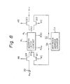
- Fig. 8 shows a circuit diagram of addressing circuitry of a DRAM embodying the present invention
- Fig. 9 shows a timing chart for each clock signal of Fig. 7 during a read/write mode
- Fig. 10 shows a timing chart for each clock signal of Fig. 7 during a refresh mode
- Fig. 11 shows a circuit diagram of clock signal generating circuitry of a further DRAM embodying the present invention
- Fig. 12 shows a circuit diagram of addressing circuitry of the further DRAM embodying the present invention
- Fig. 13 shows a timing chart for each clock signal of Fig. 11 during a read/write mode
- Fig. 14 shows a timing chart for each clock signal of Fig. 11 during a refresh mode
- Fig. 15 shows a schematic block diagram of a DRAM embodying the present invention.
- RAS denotes a row address strobe signal, CAS a column address strobe signal, and ⁇ A, ⁇ B, ⁇ C and ⁇ L internal clock signals.
- TG1 and TG2 denote gate transistors, and TR1 to TR4 transistors.
- reference numbers 15 and 16 denote input terminals, 17 a RAS buffer, and 18 and 19 inverters.
- V CC denotes a first power source and GND a second power source, i.e. ground.
- the signals RAS and CAS are input from an external circuit of the DRAM to the input terminals 15 and 16 for setting the read/write mode and the refresh mode.
- the clocks ⁇ A and ⁇ L are generated from the RAS buffer 17 after a predetermined delay time. In this case, the delay time of the clock ⁇ A is different from that of the clock ⁇ L, as explained below.
- the clock ⁇ B is obtained from a common node of the transistors TR2 and TR4, and the clock ⁇ C is obtained from a common node of the transistors TR1 and TR3. That is, when the transistor TR2 is ON and the transistor TR4 is OFF, the clock ⁇ B is at a high level. When the transistor TR1 is ON and the transistor TR3 is OFF, the clock ⁇ C is at a high level as explained below.
- AL denotes an address latch circuit constituted by, for example, flip-flop circuits
- CU denotes a refresh address counter
- N1 denotes a first input connection point (first node)
- N2 a second input connection point (second node)
- Q1 to Q8 denote transistors constituting a peripheral circuit.
- a n denotes an input address signal (TTL level) from an external stage (not shown), Q n a refresh address signal from the refresh address counter CU, Q n a complementary refresh address signal of the signal Q n , RA n a latched address signal (MOS level) from the address latch circuit AL, RA n a complementary latched address signal (MOS level) of the signal RA n , and V rf a reference voltage level (approximately, 1.5 volts) generated from the internal circuit (not shown).
- the clocks ⁇ B, ⁇ C and ⁇ L are input from the clock generator shown in Fig. 1. In this case, the clock ⁇ L is used for activating the address latch circuit AL, the clock ⁇ B for controlling the input address signal A n , and the clock ⁇ C for controlling the refresh address signals Q n and Q n .
- the charge of the node N1 is discharged in correspondence with the data of the external address signal A n through the transistors Q1 and Q3 when the clock ⁇ B is high.
- the charge of the node N2 is discharged through the transistors Q6 and Q8.
- the reference voltage V rf is set to an intermediate level of an amplitude of the input address signal A n , the discharge quantity of the node N2 is different from that of the node N1.
- the external address signal A n can be taken into the address latch circuit AL.
- the charge of the node N1 is discharged in correspondence with the signal Q n from the refresh counter CU through the transistors Q2 and Q4 when the clock ⁇ C is high.
- the charge of the node N2 is discharged in correspondence with the signal Q n from the refresh counter CU through the transistors Q5 and Q7.
- the row address strobe RAS and the column address strobe CAS are taken to be the respective trailing edges of the strobe signal waveform.
- the clock ⁇ A is obtained from the RAS buffer 17 and this clock is delayed by a predetermined delay time from the trailing edge of the signal RAS .
- the timing chart of Fig. 5 denotes the read/write mode, hereinafter called the "normal cycle", wherein t CRS denotes a set-up time of the signal CAS to signal RAS , and t RCD is a delay time between the signal RAS and the signal CAS .
- the timing chart of Fig. 6 denotes the refresh mode, hereinafter called the "CBR refresh cycle" where "CBR" means that the signal CAS is dropped from a high level to a low level before the signal RAS has dropped from a high level to a low level.
- CBR the refresh mode
- t FCS denotes a set-up time of the signal CAS to the signal RAS for the refresh operation
- t FCH denotes a hold time of the signal CAS from the signal RAS for the refresh operation.
- the row address strobe signal RAS is changed from high level (H) to low level (L) when the row address signal is taken in from the external stage.
- the column address strobe signal CAS is held at the high level.
- the signal CAS is changed from high level to low level before the signal RAS is changed from high level to low level. This trailing timing of the signal CAS is detected in the clock generator shown in Fig. 1 and the generated clock ⁇ C is input to the transistors Q2 and Q5 shown in Fig. 2.
- the clock ⁇ A rises from low level to high level after a predetermined delay time from the trailing edge of the signal RAS .
- the clock ⁇ A is input to the transistors TR1 and TR2 shown in Fig. 1.
- the address latch circuit AL is constituted by, for example, flip-flop circuits as explained above. Therefore, the transistors Q1 to Q8 are provided for forming current paths to discharge the charge in the flip-flop circuits.
- the node N1 is connected to the ground GND through either a first current path, consisting of the transistors Q1 and Q3, or a second current path, consisting of the transistors Q2 and Q4.
- the node N2 is connected to the ground GND through either a third current path, consisting of the transistors Q5 and Q7, or a fourth current path, consisting of the transistors Q6 and Q8.
- the transistors Q1 and Q6 When the clock ⁇ B is input to the transistors Q1 and Q6, these transistors are turned ON.
- the transistor Q3 is turned ON or OFF in correspondence with the high or low level of the input address signal A n .
- the transistor Q3 when the transistor Q3 is turned ON, the charge of the node N1 is completely discharged to the ground GND. Since the reference voltage V rf is set to an intermediate level between the high level and the low level at the input address signal A n , the transistor Q8 is not completely turned ON so that the discharge quantity from the node N2 is smaller than that of the node N1. Consequently, when the transistor Q3 is completely turned ON, the node N1 is discharged and becomes low level.
- the node N1 When the transistor Q3 is completely turned OFF, the node N1 is held at the high level. At this time, the node N2 is discharged and becomes low level since the transistor Q8 is turned ON at the intermediate state (i.e. incomplete turning ON state). As a result, the external address signal A n is latched in the address latch circuit AL and the data based on the latched address signal is output in correspondence with the clock ⁇ L based on the row address signal RA n or the complementary signal RA n from the circuit AL.
- the clock ⁇ C rises from low level to high level as shown in Fig. 4. That is, in Fig. 1, since the signal CAS is low, the output of the inverter 18 is high so that the transistor TR4 is turned ON. But, since the output of the inverter 19 is low, the transistor TR3 is turned OFF. Further, the transistor TR1 is turned ON and the transistor TR2 is turned OFF. Therefore, the clock ⁇ C is high and the clock ⁇ B is low.
- the clock ⁇ C is input to the transistors Q2 and Q5. Therefore, these transistors Q2 and Q5 are turned ON.
- the transistor Q4 is turned ON and the transistor Q7 is turned OFF when the refresh address signal Q n is high and the complementary refresh address signal Q n is low. Further, the transistor Q7 is turned ON and the transistor Q4 is turned OFF when the signal Q n is low and the signal Q n is high.
- the charge of the node N1 is discharged and becomes low level when the transistor Q4 is turned ON.
- the charge of the node N2 is discharged and becomes low level when the transistor Q7 is turned ON. Consequently, the refresh address signal from the counter CU is taken into the address latch circuit AL.
- the data based on the latched refresh address signal is output in correspondence with the clock ⁇ L based on the row address signal RA n and the complementary signal RA n .
- the row address strobe signal RAS is the earliest clock, based on the system operation speed.
- the column address strobe signal CAS must be input before the signal RAS is input. Therefore, some problems arise regarding this early input timing of the signal CAS . For example, it is not obvious whether or not the level of the CAS to be input is high in an initial state of a central processing unit (CPU). Therefore, a delay of approximately 50 nanoseconds occurs for inputting the signal CAS , since the signal CAS is input after determination by the CPU. Consequently, it is very difficult to achieve a high speed operation of the DRAM, owing to these delay times for the set-up time.
- CPU central processing unit
- a dynamic random access memory having improved refresh timing, which embodies the present invention will be explained in detail hereinafter.
- INV 1 to INV 6 denote inverters.
- AND 1 to AND 3 denote AND gates.
- the signal RAS is delayed by a plurality of inverters INV 1 to INV 4 and the clock ⁇ A is obtained from the inverter INV 4.
- the inverters INV 1 to INV 4 correspond to the RAS buffer 17 shown in Fig. 1.
- an inverted RAS signal (RAS) delayed by the inverters INV 1 to INV 2 is input to one input terminal of the gate AND 1.
- the signal CAS is inverted to an opposite level signal CAS in the other input terminal of the gate AND 1. Therefore, the signal CAS is obtained when the signal CAS is low. In this case, the signal RAS is always high.
- An internal clock ⁇ X is obtained by inverting the signal CAS. Therefore, the clock ⁇ C is obtained through the gate AND 2 when the clock ⁇ A and the signal CAS are high.
- the clock ⁇ B is obtained through the gate AND 3 when both clocks ⁇ A and ⁇ X are high.
- the clock ⁇ L is obtained through a NOR gate and the inverter INV 6, except when both clocks ⁇ B and ⁇ C are low. Further, many loads, for example, capacitive loads of other clock generators, are shown by a dotted line L.
- the gate AND 1 and the loading circuitry L together constitute signal modifying means. The signal CAS is sent to these loads so that the leading edge of the signal CAS becomes a gentle slope, as shown by a dotted line in Fig. 10. The present invention utilizes this gentle slope of the signal CAS. The operation of this circuit will be explained in detail hereinafter.
- Q9 to Q12 denote transistors.
- the external input address signal A n is input to an input terminal 20.
- the signals A n , V rf , Q n and Q n are input to either the source or the drain side of transistors Q9 to Q12 respectively. Conventionally, these signals are input to the gate side of each transistor as shown in Fig. 2. Therefore, each of transistors Q9 to Q12 is used only as a gate transistor.
- the transistor Q9 is used for taking in the external address signal A n when the clock ⁇ B is high in the normal cycle; the transistor Q10 is used for taking in the reference voltage V rf when the clock ⁇ B is high in the normal cycle; the transistor Q11 is used for taking in the internal refresh address signal Q n when the clock ⁇ C is high in the CBR refresh cycle; and the transistor Q12 is used for taking in the complementary refresh address signal Q n when the clock ⁇ C is high in the CBR refresh cycle.
- the clock ⁇ B is generated from the gate AND 3 when both clocks ⁇ A and ⁇ X are high. That is, the signal CAS is high in the normal cycle, and the signal CAS generated from the gate AND 1 is low since the signal RAS is high. Therefore, the internal clock ⁇ X is high so that the clock ⁇ B is output from the gate AND 3, since the clock ⁇ A is high. In this case, the clock ⁇ C from the gate AND 2 is low, since the clock ⁇ A is high and the signal CAS is low. Therefore, the clock ⁇ L is output through the NOR gate and the inverter INV 6 when the clock ⁇ B is high.
- the clock ⁇ C is generated from the gate AND 2 when the signal CAS and the clock ⁇ A are high. That is, the signal CAS is low in the CBR refresh cycle, and the signal CAS is high since the signal RAS is high. In this case, the clock ⁇ B is low, since the clock ⁇ A is high and the clock ⁇ X is low. Therefore, the clock ⁇ L is output through the NOR gate and the inverter INV 6 when the clock ⁇ C is high.
- the starting point of the leading edge of the signal CAS is earlier than that of the clock ⁇ A.
- the time at which it is completely raised is later than that of the clock ⁇ A. That is, the leading edge of the signal CAS becomes a gentle slope caused by many loads. Therefore, the time when the clock ⁇ A and the signal CAS become high level is delayed so that the leading time of the clock ⁇ C depends on the leading edge of the signal CAS. This is because, as explained above, many loads, for example capacitive loads (see Fig. 7), are provided to the output of the gate AND 1 for utilizing the signal CAS.
- the difference of the leading time between the clock ⁇ B and the clock ⁇ C is utilized. That is, in the normal cycle shown in Fig. 9, the clock ⁇ B immediately rises since the internal clock ⁇ X is high because the signal CAS is low. But, in the CBR refresh cycle, the clock ⁇ C rises after the signal CAS is completely raised for the above explained reason, although the clock ⁇ A has already risen. Therefore, each of the gate transistors Q9 to Q12 shown in Fig. 8 is opened in correspondence with the input timing of these clocks ⁇ B and ⁇ C in the normal and the CBR refresh cycles.
- the timing of the clock ⁇ B is the same as that of the clock ⁇ C, so that the inverters 18 and 19 are necessary. Therefore, it is necessary to set the refresh set-up time t FCS to a time sufficient to cover the delay time caused by these inverters 18 and 19 in the previously-considered clock generator.
- CMOS complementary metal oxide semiconductor
- the circuit can be operated by either a negative or a positive logic. But, in the case of the N-channel transistor, the circuit can be operated only by a positive logic. In general, the negative logic is better than the positive logic because the trailing operation of the signal is easier than the leading operation of the signal.
- AE denotes a delay signal delayed from the signal RAS
- ALE a control signal for controlling generation of the clocks ⁇ B and ⁇ C
- Q13 and Q15 P-channel MOS transistors and Q14 and Q16 N-channel MOS transistors.
- the pair of transistors Q 13 and Q 14 and the pair of transistors Q15 and Q16 constitute respective CMOS inverters.
- the clock ⁇ A is obtained from the signal AE after a delay by inverters INV 7 and INV 8. This clock ⁇ A is input to the source of the transistors Q14 and Q16.
- the clock ⁇ B is obtained from a common node of the transistors Q13 and Q14, and the clock ⁇ C is obtained from a common node of the transistors Q15 and Q16.
- the clocks ⁇ B and ⁇ C are input to the NAND gate, to achieve a quick operation of the NAND gate.
- 21 denotes an address buffer comprising a NAND gate NAND 2 and an inverter INV 13.
- the address buffer 21 amplifies the external address signal A n having a TTL level voltage to a clock AI n having a MOS level voltage in correspondence with the timing of the signal AE.
- the clock AI n is input to the address latch circuit AL and the complementary clock AI n inverted by the inverter INV 14 is also input to the address latch circuit AL.
- the node N1 is high.
- the clock ⁇ A also drops from a high level to a low level after a delay due to the two inverters INV7 and INV8. Therefore, the clock ⁇ B becomes low level since the clock ⁇ A is input to the source S of the transistor Q14.
- the signal ALE becomes high level after delay due to the inverters INV9 and INV10 and the gate NAND1
- the node N1 becomes low level through the gate NOR and the clock ⁇ B becomes high level (not shown).
- the clock ⁇ B functions as "one shot pulse" only the curve from high level to low level is shown in Fig. 13.
- the node N2 is low.
- the signal CAS becomes high level before the signal AE becomes low level
- the node N2 becomes high level and, then the node N1 becomes low level.
- the clock ⁇ A also becomes low level so that the clock ⁇ C becomes low level through the source S of the transistor Q16.
- the signal ALE becomes high level
- the node N2 becomes low level so that the clock ⁇ C becomes high level (not shown).
- the clock ⁇ C functions as "one shot pulse", only the curve from high level to low level is shown in Fig. 14.
- a MOS (metal oxide semiconductor) DRAM embodying the present invention comprises: a first clock generator 1 for generating clocks, for example ⁇ A, RAS, AE, etc.; a second clock generator 2A for generating clocks, for example, ⁇ B, ⁇ C, ⁇ L, ALE, etc.
- a third clock generator 2B for generating clocks to control read/write operations for a column address; a write clock generator 3 for controlling a read/write mode based on an input write enable signal WE ; a refresh control circuit 4 for generating a clock ⁇ O to control the operation of the internal refresh counter in the CBR refresh cycle; an address counter for generating an internal address signal for a refresh operation; an address buffer for a column side 6A and an address buffer for a row side 7A, each converting an input address level to an internal CMOS level; an address latch circuit for a column side 6B and an address latch circuit for a row side 7B, each latching an external address signal and a refresh address signal; a data input buffer 12 for converting the level of an input data D IN to an internal CMOS level; a data output buffer 13 for amplifying an output data D OT ; a substrate bias generator 14 for generating a back bias voltage; a memory cell array constituted by a plurality of DRAM cells; row and
Description
- The present invention relates to a semiconductor memory device, and more particularly, to a dynamic random access memory (DRAM).
- In a DRAM, the data is stored in a capacitor of a memory cell on the basis of whether or not there is a charge in the capacitor. Accordingly, the data must be refreshed to hold it in the capacitor, since the data will be lost with the elapse of time, due to a leakage of current from the capacitor.
- Therefore, a DRAM is set to operate in two modes, i.e. a read/write mode for reading or writing the data, and a refresh mode for refreshing the data. Although the operational speed of such a DRAM depends on the read/write and the refresh operational speeds at those modes, the timing of the refresh mode particularly can be an important factor in determining the operational speed of the DRAM.
- Accordingly, it is desirable to provide a dynamic random access memory having improved refresh timing, with a view to increasing the operational speed of the DRAM.
- According to the present invention, there is provided a dynamic random access memory comprising: a plurality of dynamic-type memory cells, arranged in rows and columns, for storing respective items of data; refresh control circuitry for causing the data in selected ones of those memory cells to be refreshed, when the memory is in a refresh mode, and including refresh address circuitry for generating refresh address signals denoting memory cells to be refreshed; and clock signal generating circuitry connected to receive row address strobe signals and column address strobe signals and operating in dependence thereon to generate a first clock signal, when a preset length of time has elapsed after receipt of a row address strobe signal , and to generate second and third clock signals in response to the said first clock signal, the said second clock signal being generated during a read/write mode of the memory and being delivered to addressing circuitry of the memory so as to cause that circuitry to latch an external address signal supplied thereto, and the said third clock signal being generated during the said refresh mode and being delivered to the said addressing circuitry, so as to cause that circuitry to latch a refresh address signal supplied thereto;
characterised in that the said clock signal generating circuitry includes signal modifying means including loading circuitry operative during the said refresh mode, said loading circuitry reducing the rate of change of an intermediate signal derived from the column address strobe signal and employed to determine the timing of the said third clock signal, thereby to cause the time delay between the said first and third clock signals, during the said refresh mode, to be greater than that between the said first and second clock signals during the said read/write mode. - Reference will now be made, by way of example, to the accompanying drawings, in which:
Fig. 1 shows a circuit diagram of a clock generator previously considered by the present applicants;
Fig. 2 shows a circuit diagram of an address latch circuit and peripheral circuits previously considered by the present applicants;
Fig. 3 shows a timing chart for each clock signal of Fig. 1 during a read/write mode;
Fig. 4 shows a timing chart for each clock signal of Fig. 1 during a refresh mode;
Fig. 5 shows a chart for explaining timing of row and column address strobe signals in the read/write mode;
Fig. 6 shows a chart for explaining timing of row and column address strobe signals in the refresh mode;
Fig. 7 shows a circuit diagram of clock signal generating circuitry of a DRAM embodying the present invention;
Fig. 8 shows a circuit diagram of addressing circuitry of a DRAM embodying the present invention;
Fig. 9 shows a timing chart for each clock signal of Fig. 7 during a read/write mode;
Fig. 10 shows a timing chart for each clock signal of Fig. 7 during a refresh mode;
Fig. 11 shows a circuit diagram of clock signal generating circuitry of a further DRAM embodying the present invention;
Fig. 12 shows a circuit diagram of addressing circuitry of the further DRAM embodying the present invention;
Fig. 13 shows a timing chart for each clock signal of Fig. 11 during a read/write mode;
Fig. 14 shows a timing chart for each clock signal of Fig. 11 during a refresh mode; and
Fig. 15 shows a schematic block diagram of a DRAM embodying the present invention. - Before describing the preferred embodiments, an explanation will be given of read/write and refresh timing in a DRAM previously considered by the present applicants.
- In the clock signal generator illustrated in Fig. 1,
RAS denotes a row address strobe signal,CAS a column address strobe signal, and ØA, ØB, ØC and ØL internal clock signals. TG1 and TG2 denote gate transistors, and TR1 to TR4 transistors. Further,reference numbers - The signals
RAS andCAS are input from an external circuit of the DRAM to theinput terminals RAS buffer 17 after a predetermined delay time. In this case, the delay time of the clock ØA is different from that of the clock ØL, as explained below. The clock ØB is obtained from a common node of the transistors TR2 and TR4, and the clock ØC is obtained from a common node of the transistors TR1 and TR3. That is, when the transistor TR2 is ON and the transistor TR4 is OFF, the clock øB is at a high level. When the transistor TR1 is ON and the transistor TR3 is OFF, the clock øC is at a high level as explained below. - In Fig. 2, AL denotes an address latch circuit constituted by, for example, flip-flop circuits, and CU denotes a refresh address counter. N1 denotes a first input connection point (first node), and N2 a second input connection point (second node). Q1 to Q8 denote transistors constituting a peripheral circuit. An denotes an input address signal (TTL level) from an external stage (not shown), Qn a refresh address signal from the refresh address counter CU,
Qn a complementary refresh address signal of the signal Qn , RAn a latched address signal (MOS level) from the address latch circuit AL,RAn a complementary latched address signal (MOS level) of the signal RAn , and Vrf a reference voltage level (approximately, 1.5 volts) generated from the internal circuit (not shown). The clocks øB, øC and øL are input from the clock generator shown in Fig. 1. In this case, the clock øL is used for activating the address latch circuit AL, the clock øB for controlling the input address signal An , and the clock øC for controlling the refresh address signals Qn andQn . - In the read/write mode, the charge of the node N1 is discharged in correspondence with the data of the external address signal An through the transistors Q1 and Q3 when the clock øB is high. The charge of the node N2 is discharged through the transistors Q6 and Q8. In this case, since the reference voltage Vrf is set to an intermediate level of an amplitude of the input address signal An , the discharge quantity of the node N2 is different from that of the node N1. As a result, the external address signal An can be taken into the address latch circuit AL.
- In the refresh mode, the charge of the node N1 is discharged in correspondence with the signal Qn from the refresh counter CU through the transistors Q2 and Q4 when the clock øC is high. The charge of the node N2 is discharged in correspondence with the signal
Qn from the refresh counter CU through the transistors Q5 and Q7. - With reference to Figs. 3 and 4, in which the ordinate V denotes voltage and the abscissa t denotes time, the row address strobe
RAS and the column address strobeCAS are taken to be the respective trailing edges of the strobe signal waveform. The clock øA is obtained from theRAS buffer 17 and this clock is delayed by a predetermined delay time from the trailing edge of the signalRAS . - The timing chart of Fig. 5 denotes the read/write mode, hereinafter called the "normal cycle", wherein tCRS denotes a set-up time of the signal
CAS to signalRAS , and tRCD is a delay time between the signalRAS and the signalCAS . - The timing chart of Fig. 6 denotes the refresh mode, hereinafter called the "CBR refresh cycle" where "CBR" means that the signal
CAS is dropped from a high level to a low level before the signalRAS has dropped from a high level to a low level. In Fig. 6, tFCS denotes a set-up time of the signalCAS to the signalRAS for the refresh operation, and tFCH denotes a hold time of the signalCAS from the signalRAS for the refresh operation. - In the normal cycle, the row address strobe signal
RAS is changed from high level (H) to low level (L) when the row address signal is taken in from the external stage. At this time, the column address strobe signalCAS is held at the high level. In the CBR refresh cycle, the signalCAS is changed from high level to low level before the signalRAS is changed from high level to low level. This trailing timing of the signalCAS is detected in the clock generator shown in Fig. 1 and the generated clock øC is input to the transistors Q2 and Q5 shown in Fig. 2. - The operations of the previously-considered normal cycle and the CBR refresh cycle are explained in detail hereinafter.
- Referring first of all to the normal cycle, in Fig. 3, the clock øA rises from low level to high level after a predetermined delay time from the trailing edge of the signal
RAS . The clock øA is input to the transistors TR1 and TR2 shown in Fig. 1. - In the normal cycle, since the signal
CAS is high, the output of theinverter 18 is low so that the transistor TR4 is turned OFF and, since the output of theinverter 19 is high, the transistor TR3 is turned ON. Further, the transistor TR1 is turned OFF and the transistor TR2 is turned ON. Therefore, the clock øB is high and the clock øC is low. The clock øB is input to the transistors Q1 and Q6 shown in Fig. 2. - In Fig. 2, the address latch circuit AL is constituted by, for example, flip-flop circuits as explained above. Therefore, the transistors Q1 to Q8 are provided for forming current paths to discharge the charge in the flip-flop circuits. As shown in the drawing, the node N1 is connected to the ground GND through either a first current path, consisting of the transistors Q1 and Q3, or a second current path, consisting of the transistors Q2 and Q4. Further, the node N2 is connected to the ground GND through either a third current path, consisting of the transistors Q5 and Q7, or a fourth current path, consisting of the transistors Q6 and Q8.
- When the clock øB is input to the transistors Q1 and Q6, these transistors are turned ON. The transistor Q3 is turned ON or OFF in correspondence with the high or low level of the input address signal An. In this case, when the transistor Q3 is turned ON, the charge of the node N1 is completely discharged to the ground GND. Since the reference voltage Vrf is set to an intermediate level between the high level and the low level at the input address signal An , the transistor Q8 is not completely turned ON so that the discharge quantity from the node N2 is smaller than that of the node N1. Consequently, when the transistor Q3 is completely turned ON, the node N1 is discharged and becomes low level. When the transistor Q3 is completely turned OFF, the node N1 is held at the high level. At this time, the node N2 is discharged and becomes low level since the transistor Q8 is turned ON at the intermediate state (i.e. incomplete turning ON state). As a result, the external address signal An is latched in the address latch circuit AL and the data based on the latched address signal is output in correspondence with the clock øL based on the row address signal
RAn or the complementary signal RAn from the circuit AL. - Referring now to the CBR refresh cycle, in this cycle the clock øC rises from low level to high level as shown in Fig. 4. That is, in Fig. 1, since the signal
CAS is low, the output of theinverter 18 is high so that the transistor TR4 is turned ON. But, since the output of theinverter 19 is low, the transistor TR3 is turned OFF. Further, the transistor TR1 is turned ON and the transistor TR2 is turned OFF. Therefore, the clock øC is high and the clock øB is low. - In Fig. 2, the clock øC is input to the transistors Q2 and Q5. Therefore, these transistors Q2 and Q5 are turned ON. The transistor Q4 is turned ON and the transistor Q7 is turned OFF when the refresh address signal Qn is high and the complementary refresh address signal
Qn is low. Further, the transistor Q7 is turned ON and the transistor Q4 is turned OFF when the signal Qn is low and the signalQn is high. The charge of the node N1 is discharged and becomes low level when the transistor Q4 is turned ON. The charge of the node N2 is discharged and becomes low level when the transistor Q7 is turned ON. Consequently, the refresh address signal from the counter CU is taken into the address latch circuit AL. The data based on the latched refresh address signal is output in correspondence with the clock øL based on the row address signal RAn and the complementary signalRAn . - As shown in Fig. 6, it is necessary to drop the signal
CAS from a high level to a low level before the signalRAS is dropped from a high level to a low level. Further, it is necessary to set the set-up time tFCS so that it is larger than the delay time caused by theinverters CAS from low level to high level before the signalRAS is dropped from high level to low level, as shown in Fig. 5. Approximately 10 to 20 nanoseconds are necessary for the set-up time tCRS. - As is well-known, the row address strobe signal
RAS is the earliest clock, based on the system operation speed. However, in the CBR refresh cycle, the column address strobe signalCAS must be input before the signalRAS is input. Therefore, some problems arise regarding this early input timing of the signalCAS . For example, it is not obvious whether or not the level of theCAS to be input is high in an initial state of a central processing unit (CPU). Therefore, a delay of approximately 50 nanoseconds occurs for inputting the signalCAS , since the signalCAS is input after determination by the CPU. Consequently, it is very difficult to achieve a high speed operation of the DRAM, owing to these delay times for the set-up time. - A dynamic random access memory, having improved refresh timing, which embodies the present invention will be explained in detail hereinafter.
- In Fig. 7,
INV 1 to INV 6 denote inverters. AND 1 to AND 3 denote AND gates. The signalRAS is delayed by a plurality ofinverters INV 1 toINV 4 and the clock øA is obtained from theinverter INV 4. The inverters INV 1 toINV 4 correspond to theRAS buffer 17 shown in Fig. 1. However, in an embodiment of the present invitation, an invertedRAS signal (RAS) delayed by theinverters INV 1 toINV 2 is input to one input terminal of the gate AND 1. The signalCAS is inverted to an opposite level signal CAS in the other input terminal of the gate AND 1. Therefore, the signal CAS is obtained when the signalCAS is low. In this case, the signal RAS is always high. An internal clock øX is obtained by inverting the signal CAS. Therefore, the clock øC is obtained through the gate AND 2 when the clock øA and the signal CAS are high. The clock øB is obtained through the gate AND 3 when both clocks øA and øX are high. The clock øL is obtained through a NOR gate and the inverter INV 6, except when both clocks øB and øC are low. Further, many loads, for example, capacitive loads of other clock generators, are shown by a dotted line L. The gate AND 1 and the loading circuitry L together constitute signal modifying means. The signal CAS is sent to these loads so that the leading edge of the signal CAS becomes a gentle slope, as shown by a dotted line in Fig. 10. The present invention utilizes this gentle slope of the signal CAS. The operation of this circuit will be explained in detail hereinafter. - In Fig. 8, Q9 to Q12 denote transistors. The external input address signal An is input to an
input terminal 20. As is obvious from the drawing, the signals An , Vrf, Qn andQn are input to either the source or the drain side of transistors Q₉ to Q₁₂ respectively. Conventionally, these signals are input to the gate side of each transistor as shown in Fig. 2. Therefore, each of transistors Q9 to Q12 is used only as a gate transistor. That is, the transistor Q9 is used for taking in the external address signal An when the clock øB is high in the normal cycle; the transistor Q10 is used for taking in the reference voltage Vrf when the clock øB is high in the normal cycle; the transistor Q11 is used for taking in the internal refresh address signal Qn when the clock ØC is high in the CBR refresh cycle; and the transistor Q12 is used for taking in the complementary refresh address signalQn when the clock øC is high in the CBR refresh cycle. - The operation of the circuits shown in Figs. 7 and 8 will be explained in detail with reference to Figs. 9 and 10.
- In the normal cycle shown in Fig. 9, the clock øB is generated from the gate AND 3 when both clocks øA and øX are high. That is, the signal
CAS is high in the normal cycle, and the signal CAS generated from the gate AND 1 is low since the signal RAS is high. Therefore, the internal clock øX is high so that the clock øB is output from the gate AND 3, since the clock øA is high. In this case, the clock øC from the gate AND 2 is low, since the clock øA is high and the signal CAS is low. Therefore, the clock øL is output through the NOR gate and the inverter INV 6 when the clock øB is high. - In the CBR refresh cycle shown in Fig. 10, the clock øC is generated from the gate AND 2 when the signal CAS and the clock øA are high. That is, the signal
CAS is low in the CBR refresh cycle, and the signal CAS is high since the signal RAS is high. In this case, the clock øB is low, since the clock øA is high and the clock øX is low. Therefore, the clock øL is output through the NOR gate and the inverter INV 6 when the clock øC is high. - As shown by a dotted line in the drawing, the starting point of the leading edge of the signal CAS is earlier than that of the clock øA. However, the time at which it is completely raised is later than that of the clock øA. That is, the leading edge of the signal CAS becomes a gentle slope caused by many loads. Therefore, the time when the clock øA and the signal CAS become high level is delayed so that the leading time of the clock øC depends on the leading edge of the signal CAS. This is because, as explained above, many loads, for example capacitive loads (see Fig. 7), are provided to the output of the gate AND 1 for utilizing the signal CAS.
- In an embodiment of the present invention, the difference of the leading time between the clock øB and the clock øC is utilized. That is, in the normal cycle shown in Fig. 9, the clock øB immediately rises since the internal clock øX is high because the signal CAS is low. But, in the CBR refresh cycle, the clock øC rises after the signal CAS is completely raised for the above explained reason, although the clock øA has already risen. Therefore, each of the gate transistors Q9 to Q12 shown in Fig. 8 is opened in correspondence with the input timing of these clocks øB and øC in the normal and the CBR refresh cycles.
- In Fig. 8, when the clock øB is input to the transistors Q9 and Q10 in the normal mode, these transistors are turned ON so that the external address signal An is input to the address latch circuit AL through the node N1 and the reference voltage Vrf is also input to the circuit AL through the node N2. The difference voltage between the signal An and the reference voltage Vrf is detected in the circuit AL and the row address signal RAn and the complementary row address signal
RAn are output from the circuit AL in correspondence with the clock øL after this difference voltage is amplified. In this case, the clock øL is generated at the same timing in the normal and CBR refresh cycles, to obtain a stable operation of the circuit AL in these cycles. - When the clock øC is input to the transistors Q11 and Q12 in the CBR refresh cycle, these transistors are turned ON so that the refresh address signal Qn and the complementary refresh address signal
Qn are input to the circuit AL through the nodes N1 and N2. As a result, the latched row address signal RAn and the complementary signalRAn are output from the circuit AL. - In an embodiment of the present invention, it is possible to set the refresh set-up time tFCS (see Fig. 6) so that it will become zero. That is, it is possible to set the same timing of the trailing edge between the signal
RAS and the signalCAS as shown in Fig. 10. Further, it is possible to set the later timing of the trailing edge than the signalRAS . These are because theinverters 18 and 19 (see Fig. 1) are not provided in the clock generator shown in Fig. 7, since the timing of the clock øB is different from that of the clock øC. Consequently, it is possible to achieve a high speed operation of the system. As explained above, in the previously-considered clock generation shown in Fig. 1, the timing of the clock øB is the same as that of the clock øC, so that theinverters inverters - In Figs. 11 and 12, two CMOS (complementary metal oxide semiconductor) inverters are used in the clock generator, instead of the N-channel transistor used in the first embodiment shown in Fig. 7. In the case of a CMOS, the circuit can be operated by either a negative or a positive logic. But, in the case of the N-channel transistor, the circuit can be operated only by a positive logic. In general, the negative logic is better than the positive logic because the trailing operation of the signal is easier than the leading operation of the signal.
- In Fig. 11, AE denotes a delay signal delayed from the signal
RAS , ALE a control signal for controlling generation of the clocks øB and øC, Q13 and Q15 P-channel MOS transistors, and Q14 and Q16 N-channel MOS transistors. The pair of transistors Q13 and Q14 and the pair of transistors Q15 and Q16 constitute respective CMOS inverters. The clock øA is obtained from the signal AE after a delay by inverters INV 7 andINV 8. This clock øA is input to the source of the transistors Q14 and Q16. The clock øB is obtained from a common node of the transistors Q13 and Q14, and the clock øC is obtained from a common node of the transistors Q15 and Q16. The clocks øB and øC are input to the NAND gate, to achieve a quick operation of the NAND gate. - In Fig. 12, 21 denotes an address buffer comprising a
NAND gate NAND 2 and aninverter INV 13. Theaddress buffer 21 amplifies the external address signal An having a TTL level voltage to a clock AIn having a MOS level voltage in correspondence with the timing of the signal AE. The clock AIn is input to the address latch circuit AL and the complementary clockAIn inverted by theinverter INV 14 is also input to the address latch circuit AL. - The operations of the circuits shown in Figs. 11 and 12 will be explained in detail with reference to Figs. 13 and 14.
- In the normal cycle shown in Fig. 13, initially the node N1 is high. When the signal AE is dropped from a high level to a low level, the clock øA also drops from a high level to a low level after a delay due to the two inverters INV7 and INV8. Therefore, the clock øB becomes low level since the clock øA is input to the source S of the transistor Q14. Further, when the signal ALE becomes high level after delay due to the inverters INV9 and INV10 and the gate NAND1, the node N1 becomes low level through the gate NOR and the clock øB becomes high level (not shown). In the circuit shown in Fig. 11, since the clock øB functions as "one shot pulse", only the curve from high level to low level is shown in Fig. 13.
- In the CBR refresh cycle shown in Fig. 14, initially the node N2 is low. However, since the signal CAS becomes high level before the signal AE becomes low level, the node N2 becomes high level and, then the node N1 becomes low level. Further, since the signal AE becomes low level, the clock øA also becomes low level so that the clock øC becomes low level through the source S of the transistor Q16. Further, since the signal ALE becomes high level, the node N2 becomes low level so that the clock øC becomes high level (not shown). In the circuit shown in Fig. 11, since the clock øC functions as "one shot pulse", only the curve from high level to low level is shown in Fig. 14.
- As is obvious from the above, when the node N1 is high, the clock øB is output, and when the node N2 is high, the clock øC is output, in correspondence with the timing of the clock øA. In this case, as explained above, the leading time of the signal CAS becomes a gentle slope, since many loads are connected in the path of the signal CAS.
- In Fig. 15, a MOS (metal oxide semiconductor) DRAM embodying the present invention comprises: a first clock generator 1 for generating clocks, for example øA, RAS, AE, etc.; a second clock generator 2A for generating clocks, for example, øB, øC, øL, ALE, etc. to activate a row address; a third clock generator 2B for generating clocks to control read/write operations for a column address; a write clock generator 3 for controlling a read/write mode based on an input write enable signal
WE ; a refresh control circuit 4 for generating a clock øO to control the operation of the internal refresh counter in the CBR refresh cycle; an address counter for generating an internal address signal for a refresh operation; an address buffer for a column side 6A and an address buffer for a row side 7A, each converting an input address level to an internal CMOS level; an address latch circuit for a column side 6B and an address latch circuit for a row side 7B, each latching an external address signal and a refresh address signal; a data input buffer 12 for converting the level of an input data DIN to an internal CMOS level; a data output buffer 13 for amplifying an output data DOT; a substrate bias generator 14 for generating a back bias voltage; a memory cell array constituted by a plurality of DRAM cells; row and column decoders 8 and 9; and a sense amplifier - I/O gate 10.
Claims (9)
- A dynamic random access memory comprising:
a plurality (11) of dynamic-type memory cells, arranged in rows and columns, for storing respective items of data;
refresh control circuitry (4, 5) for causing the data in selected ones of those memory cells to be refreshed, when the memory is in a refresh mode, and including refresh address circuitry (5) for generating refresh address signals (Qn,Qn ) denoting memory cells to be refreshed; and
clock signal generating circuitry (1, 2A) connected to receive row address strobe signals (RAS ) and column address strobe signals (CAS ) and operating in dependence thereon to generate a first clock signal (ØA), when a preset length of time has elapsed after receipt of a row address strobe signal (RAS ), and to generate second (ØB) and third (ØC) clock signals in response to the said first clock signal (ØA), the said second clock signal (ØB) being generated during a read/write mode of the memory and being delivered to addressing circuitry (Q9, Q10, Q11, Q12, AL) of the memory so as to cause that circuitry to latch an external address signal (An) supplied thereto, and the said third clock signal (ØC) being generated during the said refresh mode and being delivered to the said addressing circuitry (Q9, Q10, Q11, Q12, AL), so as to cause that circuitry to latch a refresh address signal (Qn,Qn ) supplied thereto;
characterised in that the said clock signal generating circuitry (1, 2A) includes signal modifying means (AND1, L) including loading circuitry (L) operative during the said refresh mode, said loading circuitry reducing the rate of change of an intermediate signal (CAS) derived from the column address strobe signal (CAS ) and employed to determine the timing of the said third clock signal (ØC), thereby to cause the time delay between the said first (ØA) and third clock signals (ØC), during the said refresh mode, to be greater than that between the said first (ØA) and second clock signals (ØB) during the said read/write mode. - A memory as claimed in claim 1, further comprising strobe signal supply means connected to initiate a refresh operation of the memory by delivering the row address strobe signal (
RAS ) and the column address strobe signal (CAS ) to the clock signal generating circuitry (1, 2A) substantially simultaneously. - A memory as claimed in claim 1 or 2, wherein the said loading circuitry (L) comprises a capacitive load.
- A memory as claimed in claim 1, 2 or 3, wherein the said clock signal generating circuitry (1, 2A) further comprises a series of inverters (INV1 to INV4) having an input for receiving the said row address strobe signal (
RAS ) and having a first output, between two of the inverters (INV2, INV3), at which an inverted row address strobe signal (RAS) is provided, and a second output, at which the said first clock signal (ØA) is provided, and wherein the said signal modifying means (AND1, L) thereof further include an AND gate (AND1) connected to receive the said inverted row address strobe signal (RAS) and the said column address strobe signal (CAS ) from which signals the AND gate derives the said intermediate signal (CAS), which signal is delivered to another inverter (INV5) of the clock signal generating circuitry (1, 2A) to obtain an internal clock signal (ØX), the modified intermediate signal (CAS) and the said internal clock signal (ØX) being supplied respectively to second and third AND gates (AND2, AND3) of the clock signal generating circuitry (1, 2A), each of which second and third AND gates (AND2, AND3) also receives the said first clock signal (ØA), the said second clock signal (ØB) being provided at an output of the said third AND gate (AND3) and the said third clock signal (ØC) being provided at an output of the said second AND gate (AND2). - A memory as claimed in claim 4, wherein the said clock signal generating circuitry (1, 2A) further comprises a NOR gate (NOR), connected for receiving the said second and third clock signals (ØB, ØC), and a further inverter (INV6) having an input connected to the output of the said NOR gate (NOR), a fourth clock signal (ØL) being provided at an output of the said further inverter (INV6).
- A memory as claimed in claim 1, 2 or 3, wherein the said clock signal generating circuitry (1, 2A) further comprises a series of inverters (INV7 to INV10) connected for receiving at an output thereof an additional signal (AE) generated by delaying the row address strobe signal (
RAS ) and for providing at an output thereof the said first clock signal (ØA), a NAND gate (NAND1) connected for receiving the said first, second and third clock signals (ØA, ØB, ØC) and producing a control signal (ALE) on the basis of those clock signals, first and second CMOS inverters (Q13, Q14; Q15, Q16), each comprising a P-channel transistor (Q13; Q15) and an N-channel transistor (Q14; Q16) connected together in series, respective sources of the N-channel transistors (Q14; Q16) being connected to receive the said first clock signal (ØA), and the said second and third clock signals (ØB, ØC) being provided at respective outputs of the first and second CMOS inverters, a NOR gate (NOR) having inputs connected to receive the said control signal (ALE) and the modified intermediate signal (CAS) and an output connected to an input of the said first CMOS inverter (Q13; Q15), and a gate transistor (Q17) connected to supply the said modified intermediate signal (CAS) to an input of the said second CMOS inverter (Q14; Q16) in accordance with an inverted version of the control signal (ALE). - A memory as claimed in claim 6, wherein the said clock signal generating circuitry (1, 2A) further comprises an additional inverter (INV11) connected to receive and invert the said control signal (ALE) so as to produce a fourth clock signal (ØL).
- A memory as claimed in any preceding claim, wherein the said addressing circuitry (Q9, Q10, Q11, Q12, AL) comprises address latch means (AL), having respective first and second inputs connected to first and second nodes (N1, N2) of the circuitry, first and second gate transistors (Q9, Q10) connected to deliver an external address signal (An) and a reference signal (Vrf) to the said first and second nodes (N1, N2) respectively upon receipt of the said second clock signal (ØB), and third and fourth gate transistors (Q11, Q12) connected to deliver a refresh address signal (Qn) and a complementary refresh address signal (
Q n) to the said first and second nodes (N1, N2) upon receipt of the said third clock signal (ØC). - A memory as claimed in claim 8, when read as appended to claim 6 or 7, wherein the said addressing circuitry further comprises address buffer means (21) including a NAND gate (NAND2) and an inverter (INV13) connected together in series for converting the external address signal (An) from the TTL level voltage to the MOS level voltage in accordance with the said additional signal (AE).
Applications Claiming Priority (2)
| Application Number | Priority Date | Filing Date | Title |
|---|---|---|---|
| JP61198938A JPS6355797A (en) | 1986-08-27 | 1986-08-27 | Memory |
| JP198938/86 | 1986-08-27 |
Publications (2)
| Publication Number | Publication Date |
|---|---|
| EP0260039A1 EP0260039A1 (en) | 1988-03-16 |
| EP0260039B1 true EP0260039B1 (en) | 1991-07-10 |
Family
ID=16399465
Family Applications (1)
| Application Number | Title | Priority Date | Filing Date |
|---|---|---|---|
| EP87307618A Expired - Lifetime EP0260039B1 (en) | 1986-08-27 | 1987-08-27 | Dynamic random access memory |
Country Status (5)
| Country | Link |
|---|---|
| US (1) | US4985868A (en) |
| EP (1) | EP0260039B1 (en) |
| JP (1) | JPS6355797A (en) |
| KR (1) | KR910004732B1 (en) |
| DE (1) | DE3771288D1 (en) |
Families Citing this family (34)
| Publication number | Priority date | Publication date | Assignee | Title |
|---|---|---|---|---|
| US5313428A (en) * | 1987-11-12 | 1994-05-17 | Sharp Kabushiki Kaisha | Field memory self-refreshing device utilizing a refresh clock signal selected from two separate clock signals |
| US5031150A (en) * | 1988-08-26 | 1991-07-09 | Kabushiki Kaisha Toshiba | Control circuit for a semiconductor memory device and semiconductor memory system |
| US6212089B1 (en) * | 1996-03-19 | 2001-04-03 | Hitachi, Ltd. | Semiconductor memory device and defect remedying method thereof |
| KR0141495B1 (en) * | 1988-11-01 | 1998-07-15 | 미다 가쓰시게 | Semiconductor memory device and defect remedying method thereof |
| JP2547633B2 (en) * | 1989-05-09 | 1996-10-23 | 三菱電機株式会社 | Semiconductor memory device |
| KR940008295B1 (en) * | 1989-08-28 | 1994-09-10 | 가부시기가이샤 히다찌세이사꾸쇼 | Semiconductor memory |
| USRE38379E1 (en) * | 1989-08-28 | 2004-01-06 | Hitachi, Ltd. | Semiconductor memory with alternately multiplexed row and column addressing |
| JP3225531B2 (en) * | 1990-05-15 | 2001-11-05 | セイコーエプソン株式会社 | Memory card |
| US5260904A (en) * | 1990-05-31 | 1993-11-09 | Oki Electric Industry Co., Ltd. | Data bus clamp circuit for a semiconductor memory device |
| KR100214435B1 (en) * | 1990-07-25 | 1999-08-02 | 사와무라 시코 | Synchronous burst-access memory |
| US5144168A (en) * | 1990-08-17 | 1992-09-01 | Texas Instruments Incorporated | Self latching input buffer |
| JP3100622B2 (en) * | 1990-11-20 | 2000-10-16 | 沖電気工業株式会社 | Synchronous dynamic RAM |
| TW198135B (en) * | 1990-11-20 | 1993-01-11 | Oki Electric Ind Co Ltd | |
| JP3225533B2 (en) * | 1991-04-11 | 2001-11-05 | 日本電気株式会社 | Dynamic semiconductor memory device |
| JP3143950B2 (en) * | 1991-04-30 | 2001-03-07 | 日本電気株式会社 | Dynamic memory |
| US5255241A (en) * | 1991-05-20 | 1993-10-19 | Tandem Computers Incorporated | Apparatus for intelligent reduction of worst case power in memory systems |
| JPH04372790A (en) * | 1991-06-21 | 1992-12-25 | Sharp Corp | Semiconductor memory |
| US5289430A (en) * | 1991-11-26 | 1994-02-22 | Texas Instruments Incorporated | Self latching input buffer |
| JPH05234371A (en) * | 1992-02-21 | 1993-09-10 | Fujitsu Ltd | Dynamic ram |
| JP2982928B2 (en) * | 1992-04-01 | 1999-11-29 | 三菱電機株式会社 | Semiconductor storage device |
| JP3302726B2 (en) * | 1992-07-31 | 2002-07-15 | 株式会社東芝 | Semiconductor storage device |
| JP2739802B2 (en) * | 1992-12-01 | 1998-04-15 | 日本電気株式会社 | Dynamic RAM device |
| JPH08180678A (en) * | 1994-12-27 | 1996-07-12 | Hitachi Ltd | Dynamic ram |
| JP3710845B2 (en) | 1995-06-21 | 2005-10-26 | 株式会社ルネサステクノロジ | Semiconductor memory device |
| US5640361A (en) * | 1996-05-01 | 1997-06-17 | Hewlett-Packard Company | Memory architecture |
| US6009038A (en) * | 1996-05-31 | 1999-12-28 | United Microelectronics Corporation | Addressing unit |
| JPH09320269A (en) * | 1996-05-31 | 1997-12-12 | Nippon Steel Corp | Address device |
| JPH1139862A (en) * | 1997-07-16 | 1999-02-12 | Mitsubishi Electric Corp | Semiconductor memory device |
| JP4613378B2 (en) * | 1999-11-01 | 2011-01-19 | 富士通セミコンダクター株式会社 | Semiconductor integrated circuit |
| TW454289B (en) * | 2000-03-09 | 2001-09-11 | Taiwan Semiconductor Mfg | Programmable memory refresh architecture |
| JP2006073062A (en) * | 2004-08-31 | 2006-03-16 | Toshiba Corp | Semiconductor memory device |
| US20070038805A1 (en) * | 2005-08-09 | 2007-02-15 | Texas Instruments Incorporated | High granularity redundancy for ferroelectric memories |
| US20090175115A1 (en) * | 2008-01-09 | 2009-07-09 | Christoph Bilger | Memory device, method for accessing a memory device and method for its manufacturing |
| EP3454337B1 (en) * | 2017-09-06 | 2019-09-11 | Tu Kaiserslautern | Using runtime reverse engineering to optimize dram refresh |
Family Cites Families (13)
| Publication number | Priority date | Publication date | Assignee | Title |
|---|---|---|---|---|
| US4207618A (en) * | 1978-06-26 | 1980-06-10 | Texas Instruments Incorporated | On-chip refresh for dynamic memory |
| JPS55150192A (en) * | 1979-05-08 | 1980-11-21 | Nec Corp | Memory unit |
| JPS5897195A (en) * | 1981-12-07 | 1983-06-09 | Fujitsu Ltd | Dynamic semiconductor memory device |
| JPS58155596A (en) * | 1982-03-10 | 1983-09-16 | Hitachi Ltd | Dynamic type mos ram |
| JPS58159293A (en) * | 1982-03-17 | 1983-09-21 | Fujitsu Ltd | Memory element control system |
| US4472647A (en) * | 1982-08-20 | 1984-09-18 | Motorola, Inc. | Circuit for interfacing with both TTL and CMOS voltage levels |
| JPS5987695A (en) * | 1982-11-11 | 1984-05-21 | Toshiba Corp | Semiconductor memory device |
| JP2518810B2 (en) * | 1983-11-29 | 1996-07-31 | 富士通株式会社 | Semiconductor integrated circuit device |
| JPS60153223A (en) * | 1984-01-20 | 1985-08-12 | Ricoh Co Ltd | Input buffer circuit |
| US4575826A (en) * | 1984-02-27 | 1986-03-11 | International Business Machines Corp. | Refresh generator system for a dynamic memory |
| US4747082A (en) * | 1984-11-28 | 1988-05-24 | Hitachi Ltd. | Semiconductor memory with automatic refresh means |
| US4672243A (en) * | 1985-05-28 | 1987-06-09 | American Telephone And Telegraph Company, At&T Bell Laboratories | Zero standby current TTL to CMOS input buffer |
| JPH087995B2 (en) * | 1985-08-16 | 1996-01-29 | 富士通株式会社 | Method and apparatus for refreshing dynamic semiconductor memory device |
-
1986
- 1986-08-27 JP JP61198938A patent/JPS6355797A/en active Pending
-
1987
- 1987-08-27 EP EP87307618A patent/EP0260039B1/en not_active Expired - Lifetime
- 1987-08-27 KR KR8709415A patent/KR910004732B1/en not_active IP Right Cessation
- 1987-08-27 DE DE8787307618T patent/DE3771288D1/en not_active Expired - Fee Related
-
1989
- 1989-12-14 US US07/449,427 patent/US4985868A/en not_active Expired - Fee Related
Also Published As
| Publication number | Publication date |
|---|---|
| DE3771288D1 (en) | 1991-08-14 |
| JPS6355797A (en) | 1988-03-10 |
| US4985868A (en) | 1991-01-15 |
| KR880003333A (en) | 1988-05-16 |
| EP0260039A1 (en) | 1988-03-16 |
| KR910004732B1 (en) | 1991-07-10 |
Similar Documents
| Publication | Publication Date | Title |
|---|---|---|
| EP0260039B1 (en) | Dynamic random access memory | |
| US6188641B1 (en) | Synchronous semiconductor memory device having input circuit with reduced power consumption | |
| US6260128B1 (en) | Semiconductor memory device which operates in synchronism with a clock signal | |
| US3959781A (en) | Semiconductor random access memory | |
| US7855926B2 (en) | Semiconductor memory device having local sense amplifier with on/off control | |
| US7184362B2 (en) | Page access circuit of semiconductor memory device | |
| US4766572A (en) | Semiconductor memory having a bypassable data output latch | |
| US4087704A (en) | Sequential timing circuitry for a semiconductor memory | |
| US5555526A (en) | Synchronous semiconductor memory device having an auto-precharge function | |
| US5455803A (en) | Semiconductor device which operates at a frequency controlled by an external clock signal | |
| JPS621183A (en) | Dynamic ram | |
| US6337833B1 (en) | Memory device | |
| JPH0713857B2 (en) | Semiconductor memory device | |
| US4688196A (en) | Semiconductor dynamic memory device with less power consumption in internal refresh mode | |
| KR100225954B1 (en) | Semiconductor memory element for saving power consumption | |
| JPH09231767A (en) | Static semiconductor memory device | |
| GB2341706A (en) | Synchronous semiconductor memory device with a clock generating circuit | |
| JPH09320261A (en) | Semiconductor memory circuit and control signal generation circuit | |
| JPH10240372A (en) | Internal clock generation circuit and internal clock generation method for semiconductor device | |
| EP0409274B1 (en) | Dynamic memory with a refresh control circuit | |
| US6545924B2 (en) | Semiconductor memory device | |
| USRE36532E (en) | Synchronous semiconductor memory device having an auto-precharge function | |
| US5255223A (en) | Semiconductor memory device having alternatively operated equalizing and erasing functions | |
| US6122214A (en) | Semiconductor memory | |
| JPH04265598A (en) | Semiconductor memory |
Legal Events
| Date | Code | Title | Description |
|---|---|---|---|
| PUAI | Public reference made under article 153(3) epc to a published international application that has entered the european phase |
Free format text: ORIGINAL CODE: 0009012 |
|
| AK | Designated contracting states |
Kind code of ref document: A1 Designated state(s): DE FR GB |
|
| 17P | Request for examination filed |
Effective date: 19880427 |
|
| 17Q | First examination report despatched |
Effective date: 19891019 |
|
| GRAA | (expected) grant |
Free format text: ORIGINAL CODE: 0009210 |
|
| AK | Designated contracting states |
Kind code of ref document: B1 Designated state(s): DE FR GB |
|
| ET | Fr: translation filed | ||
| REF | Corresponds to: |
Ref document number: 3771288 Country of ref document: DE Date of ref document: 19910814 |
|
| PLBE | No opposition filed within time limit |
Free format text: ORIGINAL CODE: 0009261 |
|
| STAA | Information on the status of an ep patent application or granted ep patent |
Free format text: STATUS: NO OPPOSITION FILED WITHIN TIME LIMIT |
|
| 26N | No opposition filed | ||
| PGFP | Annual fee paid to national office [announced via postgrant information from national office to epo] |
Ref country code: GB Payment date: 19950816 Year of fee payment: 9 |
|
| PGFP | Annual fee paid to national office [announced via postgrant information from national office to epo] |
Ref country code: DE Payment date: 19950828 Year of fee payment: 9 |
|
| PGFP | Annual fee paid to national office [announced via postgrant information from national office to epo] |
Ref country code: FR Payment date: 19960809 Year of fee payment: 10 |
|
| PG25 | Lapsed in a contracting state [announced via postgrant information from national office to epo] |
Ref country code: GB Effective date: 19960827 |
|
| GBPC | Gb: european patent ceased through non-payment of renewal fee |
Effective date: 19960827 |
|
| PG25 | Lapsed in a contracting state [announced via postgrant information from national office to epo] |
Ref country code: DE Effective date: 19970501 |
|
| PG25 | Lapsed in a contracting state [announced via postgrant information from national office to epo] |
Ref country code: FR Free format text: LAPSE BECAUSE OF NON-PAYMENT OF DUE FEES Effective date: 19980430 |
|
| REG | Reference to a national code |
Ref country code: FR Ref legal event code: ST |