EP0258893A2 - Start pattern detecting apparatus - Google Patents
Start pattern detecting apparatus Download PDFInfo
- Publication number
- EP0258893A2 EP0258893A2 EP87112876A EP87112876A EP0258893A2 EP 0258893 A2 EP0258893 A2 EP 0258893A2 EP 87112876 A EP87112876 A EP 87112876A EP 87112876 A EP87112876 A EP 87112876A EP 0258893 A2 EP0258893 A2 EP 0258893A2
- Authority
- EP
- European Patent Office
- Prior art keywords
- pattern
- output
- signal
- received data
- circuit
- Prior art date
- Legal status (The legal status is an assumption and is not a legal conclusion. Google has not performed a legal analysis and makes no representation as to the accuracy of the status listed.)
- Granted
Links
Images


Classifications
-
- H—ELECTRICITY
- H04—ELECTRIC COMMUNICATION TECHNIQUE
- H04L—TRANSMISSION OF DIGITAL INFORMATION, e.g. TELEGRAPHIC COMMUNICATION
- H04L7/00—Arrangements for synchronising receiver with transmitter
- H04L7/04—Speed or phase control by synchronisation signals
- H04L7/041—Speed or phase control by synchronisation signals using special codes as synchronising signal
- H04L7/042—Detectors therefor, e.g. correlators, state machines
-
- H—ELECTRICITY
- H04—ELECTRIC COMMUNICATION TECHNIQUE
- H04L—TRANSMISSION OF DIGITAL INFORMATION, e.g. TELEGRAPHIC COMMUNICATION
- H04L12/00—Data switching networks
- H04L12/54—Store-and-forward switching systems
- H04L12/56—Packet switching systems
- H04L12/5601—Transfer mode dependent, e.g. ATM
- H04L2012/5672—Multiplexing, e.g. coding, scrambling
- H04L2012/5674—Synchronisation, timing recovery or alignment
-
- H—ELECTRICITY
- H04—ELECTRIC COMMUNICATION TECHNIQUE
- H04L—TRANSMISSION OF DIGITAL INFORMATION, e.g. TELEGRAPHIC COMMUNICATION
- H04L7/00—Arrangements for synchronising receiver with transmitter
- H04L7/04—Speed or phase control by synchronisation signals
- H04L7/041—Speed or phase control by synchronisation signals using special codes as synchronising signal
- H04L7/043—Pseudo-noise [PN] codes variable during transmission
-
- H—ELECTRICITY
- H04—ELECTRIC COMMUNICATION TECHNIQUE
- H04L—TRANSMISSION OF DIGITAL INFORMATION, e.g. TELEGRAPHIC COMMUNICATION
- H04L7/00—Arrangements for synchronising receiver with transmitter
- H04L7/04—Speed or phase control by synchronisation signals
- H04L7/10—Arrangements for initial synchronisation
Definitions
- the present invention relates to an apparatus for detecting a start pattern and, more particularly, to an apparatus for accurately detecting a start pattern in the event of reception of a digital signal in which the start pattern is followed by an data signal.
- a prerequisite with the processing of a data signal received is detecting the starting point of the data signal as defined by a start pattern.
- a start pattern therefore, has to be detected accurately without errors.
- the length of a start pattern is increased in proportion to the significance of a data signal for the purpose of promoting accurate detection of a start pattern.
- Such, however, cannot be implemented without the need for hardware of considerably large scale.
- a start pattern is provided with a substantial length so as not to detect a start pattern out of noise which is included in received data, resulting in an impracticably large circuit scale.
- an object of the present invention to provide a start pattern detecting apparatus capable of accurately detecting a start pattern included in received data in which the start pattern is followed by a data signal.
- An apparatus for detecting a start pattern included in received data in which an information signal follows the start pattern of the present invention comprises a pattern recovery circuit for recovering the start pattern, an electronic switch for selecting one of the received data and an output of the pattern recovery circuit at a time and applying the received signal or the output of the pattern recovery circuit selected to the pattern recovery circuit, a decision circuit for determining whether or not the output of the pattern recovery circuit and the received data are identical in pattern and, when decided not identical, generating a control signal for causing the electronic switch to select the received data, a match detection circuit for performing pattern matching on a pattern which is recovered by the pattern recovery circuit, and an output circuit for producing an output signal in response to an output of the match detection circuit when the decision circuit decides that the output of the pattern recovery circuit and the received data are identical in pattern.
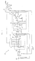
- a start pattern detecting apparatus i.e., a circuit for detecting a start pattern out of received data, shown in Fig. 1.
- a start pattern is assumed to be "11001" the number of bits n of which is five.
- the allowable number of errors r is one, meaning that a detection output is produced and fed out through an output terminal even if one bit of error is present.
- the prior art apparatus generally 10, includes a shift register 12 the number of bits n of which is five. Namely, the shift register 12 accommodates five bits of received data RD.
- AND gates 14(1) to 14(5) individually produce a (logica) ONE even if one bit of error exists in a start pattern, which is included in the received data.
- An OR gate 16 produces an ouput signal MATCH, or a ONE, when any of the AND gates 14(1) to 14(5) applies a ONE to the OR gate 16.
- Inverters 18(1) and 18(2) are provided so that when a start pattern is stored in the shift register 12, the inputs to all of the AND gates 14(1) to 14(5) may become a ONE.
- FM Frequency ModulatIon
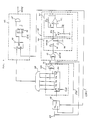
- a start pattern detecting apparatus embodying the present invention which solves the above-discussed problem is shown and generally designated by the reference numeral 20.
- the apparatus includes a pattern recovery circuit 22 which is made up of a 5-bit shift register 24 and an Exclusive-OR (EX-OR) gate 26.
- An electronic switch 28 is connected to the pattern recovery circuit 24 for selecting either one of received data and a PN (Pseudo Noise) signal which is output by the pattern recovery circuit 22.
- the electronic switch 28 is controlled by a control signal CONT which is output by a decision circuit 30. Specifically, when the PN signal from the pattern recovery circuit 22 and the received data RD are matched, the decision circuit 30 applies a (logical) ZERO to the switch 28 as the control signal CONT causing the switch 28 to select the PN signal.
- the decision circuit 30 includes an EX-OR gate 32 to which the PN signal from the pattern recovery circuit 22 and the received data RD are applied. If the PN signal and the received data RD are matched, the EX-OR gate 32 produces a ZERO on its output OUT 32.
- This output OUT 32 is routed through a resistor 36 having resistance R1 and a capacitor 38 having capacitance C1 for the purpose of suppressing fluctuation, i.e., the resistor 36 and capacitor 38 cooperate to constitute a low-pass filter (LPF) 34.
- LPF low-pass filter
- the time constant R1C1 of the LPF 34 is selected to be sufficiently greater than the time width of one bit.
- the output OUT 34 of the LPF 34 is applied to a hysteresis comparator circuit 40.
- a comparator 42 compares the input OUT 34 with a reference voltage V c .
- the result of comparison output by the comparator 42 is positively fed back via a resistor 44 having resistance R3, whereby a hysteresis characteristic is provided.
- a resistor 46 has resistance R2 which is selected to be relatively high to prevent the output of the comparator 42 from effecting the LPF 34. Specifically, when the output OUT 32 of the EX-OR gate 32 of the decision circuit 30 becomes a ZERO which is representative of a match between the PN signal and the received data RD, the output voltage OUT 34 of the filter 34, too, becomes low. This low voltage is compared with the reference voltage by the hysteresis comparator 40 which then produces a control signal CONT which is a ZERO.
- the electronic switch 28, pattern recovery circuit 22 and decision circuit 30 will be described with reference to Fig. 3. As shown, while a signal is not received, the received output is in a noise condition. In such a section, since the received data RD is entirely random, it is not always coincident with a PN signal which is output by the pattern recovery circuit 22 and, hence, the output OUT 32 of the EX-OR gate 32 changes irregularly. This cuases a higher voltage than the reference voltage to appear on the output OUT 34 of the LPF 34, whereby the hysteresis comparator 40 produces a ONE as the control signal CONT. Then, the electronic switch 28 is actuated by the control signal CONT to select the received data RD and feed it to the pattern recovery circuit 22.
- the hysteresis comparator 40 responds by delivering a ZERO to the electronic switch 28 as the control signal CONT. Then, the switch 28 selects the PN signal from the pattern recovery circuit 22 and generates a signal independently of the received data RD. If the PN signal and the received data RD continue to be identical in pattern, the output OUT 32 of the EX-OR gate 32 and, therefore, the output CONT of the decision circuit 30 remains to be ZERO maintaining the switch 28 in the existing condition.
- the received data RD may be regarded to be a start pattern which is constituted by the five-stage PN signal.
- the received data RD may involve an error, an error does not occur in the PN signal output by the pattern recovery circuit 22 at all. It follows that error-free detection is achievable if a match is detected by a match detection circuit 48 with regard to the content of the pattern recovery circuit 22, i.e. outputs Q1 to Q5 of the shift register 24.
- the match detection circuit 48 is implemented with an AND gate which produces a match output when all the contents of the shift register 24 are a ONE. The number of inputs of the AND gate 48 need only be equal to that of the bits of the shift register 24.
- the match output is routed through an output circuit 50 to be delivered as an output signal MATCH.
- the output circuit 50 consists of an inverter 52 and an AND gate 54 and passes the output of the match detection circuit 48 when the control signal CONT is a ZERO.
- FIG. 4 another embodiment of the present invention is shown. Since the embodiment of Fig. 4 is essentially similar to that of Fig. 2 except for the construction of the output circuit 50, the following description will mainly concentrate on the output circuit.
- the match detection circuit 48 produces a match output when all the contents of the shift register 24 are a ONE, the match output being delivered via an output circuit 62.
- the output circuit 62 responds only to the first match output of the match detection circuit 48 by producing an output signal MATCH which is a ONE.
- MATCH which is a ONE.
- a set-reset circuit 64 of the output circuit 52 is reset to produce a ONE.
- a flip-flop 66 has a non-inverting output Q which is a ZERO and an inverting output which is a ONE.
- a match between the PN signal and the received data RD has thereafter occurred to turn the control signal CONT into a ZERO.
- the set-reset circuit 64 produces a ONE.
- the inverting output of the flip-flop 66 is operated by a clock CLK and remains to be a ONE for the duration of one bit, so that a ONE is fed out via an AND gate 68 as the signal MATCH. After one bit as counted from the change of the output of the set-reset circuit 64 to a ONE, the inverting output of the flip-flop 66 becomes a ZERO and, hence, the output MATCH of the AND gate 68 remains to be a ZERO thereafter.
- control signal CONT continues to be a ZERO, even if the output of the match detection circuit 48 is changed to a ONE, the output circuit 62 does not respond and continuously produces a ZERO as the output signal MATCH because the output of the set-reset circuit 64 is still a ZERO.
- a start pattern which is a five-stage PN pattern having thirty-one bits. Even if a considerably long start pattern such as a one having 1,000 bits is used, all that is required is increasing the number of stages of the shift register 24 to ten, i.e., it is needless to scale up the circuit to a noticeable extent.
- the pattern recovery circuit 22 since the pattern recovery circuit 22 recovers a start pattern timed to received data RD and since match detection is performed on the pattern recovery circuit 22, the detection is not directly related to bit errors which may exist in received data RD. This allows a minimum of erroneous processing to occur.
- the decision circuit 30 is shown as comprising the LPF 34 and hysteresis comparator 40 which are analog devices, such is merely to facilitate the understanding.
- the LPF 34 may be replaced with an up-down counter, and the hysteresis converter 40 with a digital comparator.
- the up-down counter will be constructed to up-count when the output OUT 32 of the EX-OR gate 32 is a ONE and down-count when it is a ZERO.
- the present invention provides a start pattern detecting apparatus which is capable of detecting a start pattern without errors even if the start pattern is considerably long and, yet, with a far smaller circuit scale than the prior art. Further, since the detection of a start pattern is performed only once while a start pattern is received, a pattern analogous to a start pattern which may be included in a subsequent information signal is prevented from causing a pattern match output to respond any further.
Abstract
Description
- The present invention relates to an apparatus for detecting a start pattern and, more particularly, to an apparatus for accurately detecting a start pattern in the event of reception of a digital signal in which the start pattern is followed by an data signal.
- A prerequisite with the processing of a data signal received is detecting the starting point of the data signal as defined by a start pattern. A start pattern, therefore, has to be detected accurately without errors. Usually, the length of a start pattern is increased in proportion to the significance of a data signal for the purpose of promoting accurate detection of a start pattern. Such, however, cannot be implemented without the need for hardware of considerably large scale. Specifically, in a prior art apparatus for the detection of a start pattern, a start pattern is provided with a substantial length so as not to detect a start pattern out of noise which is included in received data, resulting in an impracticably large circuit scale.
- It is, therefore, an object of the present invention to provide a start pattern detecting apparatus capable of accurately detecting a start pattern included in received data in which the start pattern is followed by a data signal.
- It is another object of the present invention to provide a start pattern detecting apparatus having a simple circuit arrangement.
- It is another object of the present invention to provide a generally improved start pattern detecting apparatus.
- An apparatus for detecting a start pattern included in received data in which an information signal follows the start pattern of the present invention comprises a pattern recovery circuit for recovering the start pattern, an electronic switch for selecting one of the received data and an output of the pattern recovery circuit at a time and applying the received signal or the output of the pattern recovery circuit selected to the pattern recovery circuit, a decision circuit for determining whether or not the output of the pattern recovery circuit and the received data are identical in pattern and, when decided not identical, generating a control signal for causing the electronic switch to select the received data, a match detection circuit for performing pattern matching on a pattern which is recovered by the pattern recovery circuit, and an output circuit for producing an output signal in response to an output of the match detection circuit when the decision circuit decides that the output of the pattern recovery circuit and the received data are identical in pattern.
- The above and other objects, features and advantages of the present invention will become more apparent from the following detailed description taken with the accompanying drawings.
-
- Fig. 1 is a circuit diagram showing a prior art start pattern detecting apparatus;
- Fig. 2 is a circuit diagram showing a start pattern detecting apparatus in accordance with the present invention;
- Fig. 3 is a timing chart demonstrating the operation of the apparatus as shown in Fig. 2; and
- Fig. 4 is a circuit diagram showing another embodiment of the present invention.
- To better understand the present invention, a brief reference will be made to a prior art start pattern detecting apparatus, i.e., a circuit for detecting a start pattern out of received data, shown in Fig. 1. For the simplicity of description, a start pattern is assumed to be "11001" the number of bits n of which is five. In this particular example, the allowable number of errors r is one, meaning that a detection output is produced and fed out through an output terminal even if one bit of error is present. In detail, the prior art apparatus, generally 10, includes a shift register 12 the number of bits n of which is five. Namely, the shift register 12 accommodates five bits of received data RD. AND gates 14(1) to 14(5) individually produce a (logica) ONE even if one bit of error exists in a start pattern, which is included in the received data. An
OR gate 16 produces an ouput signal MATCH, or a ONE, when any of the AND gates 14(1) to 14(5) applies a ONE to theOR gate 16. Inverters 18(1) and 18(2) are provided so that when a start pattern is stored in the shift register 12, the inputs to all of the AND gates 14(1) to 14(5) may become a ONE. - Although the apparatus of Fig. 1 may readily be implemented because the number of bits n of the start pattern is as small as five, the probability that it decides received data RD which is not a start pattern to be a start pattern is considerably high. Assume that noise comes in as the received data RD despite that a signal is not being received; in the case of an FM (Frequency ModulatIon) receiver, a noise condition is developed while the receiver is not receiving a signal. Then, the rate Pd at which the prior art apparatus detects a 5-bit pattern out of entirely random noise under the one-bit allowability condition is expressed as:
Pd = 1/2⁵ + 5 x 2⁵ = 3/16
This implies that the false detection stated above occurs three times per sixteen bits. Hence, despite that no signal is being received, the apparatus detects a start pattern included in noise with a high probability, resulting in erroneous processing. - In the light of this, there may be used a start pattern the number of bits n of which is 100, and an allowable number r of error bits which is three. In this instance, the probability Pd that a start pattern is found in a noise condition is produced by:
Pd = 1/2¹⁰⁰ + ₁₀₀C₁/2¹⁰⁰ + ₁₀₀C₂/2¹⁰⁰ + ₁₀₀C₃/2¹⁰⁰
≃ ₁₀₀C₃/2¹⁰⁰ ≃ 1.6 x 10⁻⁵
Thus, the probability of false detection is low. However, as regards a circuit for implementing such an approach, the AND gates 14(1) to 14(5) shown in Fig. 1 have to be replaced with as many as 161,700 (¹⁰⁰C₃) AND gates each having 97 inputs, resulting in a prohibitively large circuit scale. - Referring to Fig. 2, a start pattern detecting apparatus embodying the present invention which solves the above-discussed problem is shown and generally designated by the
reference numeral 20. As shown, the apparatus includes apattern recovery circuit 22 which is made up of a 5-bit shift register 24 and an Exclusive-OR (EX-OR)gate 26. Anelectronic switch 28 is connected to thepattern recovery circuit 24 for selecting either one of received data and a PN (Pseudo Noise) signal which is output by thepattern recovery circuit 22. In this particular embodiment, when theelectronic switch 28 selects the PN signal from thepattern recovery circuit 22, thepattern recovery circuit 22 produces a 5-bit PN signal (period = 2⁵ - 1 = 31 bits). Theelectronic switch 28 is controlled by a control signal CONT which is output by adecision circuit 30. Specifically, when the PN signal from thepattern recovery circuit 22 and the received data RD are matched, thedecision circuit 30 applies a (logical) ZERO to theswitch 28 as the control signal CONT causing theswitch 28 to select the PN signal. - The
decision circuit 30 includes an EX-ORgate 32 to which the PN signal from thepattern recovery circuit 22 and the received data RD are applied. If the PN signal and the received data RD are matched, the EX-ORgate 32 produces a ZERO on itsoutput OUT 32. Thisoutput OUT 32 is routed through aresistor 36 having resistance R₁ and acapacitor 38 having capacitance C₁ for the purpose of suppressing fluctuation, i.e., theresistor 36 andcapacitor 38 cooperate to constitute a low-pass filter (LPF) 34. Here, the time constant R₁C₁ of theLPF 34 is selected to be sufficiently greater than the time width of one bit. Theoutput OUT 34 of theLPF 34 is applied to ahysteresis comparator circuit 40. In thiscircuit 40, acomparator 42 compares theinput OUT 34 with a reference voltage Vc. The result of comparison output by thecomparator 42 is positively fed back via aresistor 44 having resistance R₃, whereby a hysteresis characteristic is provided. Aresistor 46 has resistance R₂ which is selected to be relatively high to prevent the output of thecomparator 42 from effecting theLPF 34. Specifically, when theoutput OUT 32 of the EX-ORgate 32 of thedecision circuit 30 becomes a ZERO which is representative of a match between the PN signal and the received data RD, theoutput voltage OUT 34 of thefilter 34, too, becomes low. This low voltage is compared with the reference voltage by thehysteresis comparator 40 which then produces a control signal CONT which is a ZERO. - The operations of the
electronic switch 28,pattern recovery circuit 22 anddecision circuit 30 will be described with reference to Fig. 3. As shown, while a signal is not received, the received output is in a noise condition. In such a section, since the received data RD is entirely random, it is not always coincident with a PN signal which is output by thepattern recovery circuit 22 and, hence, theoutput OUT 32 of the EX-ORgate 32 changes irregularly. This cuases a higher voltage than the reference voltage to appear on theoutput OUT 34 of theLPF 34, whereby thehysteresis comparator 40 produces a ONE as the control signal CONT. Then, theelectronic switch 28 is actuated by the control signal CONT to select the received data RD and feed it to thepattern recovery circuit 22. - The operation will be further described on the assumption that a 5-stage PN pattern "0001101110101000010010110011111" is received as a start pattern by way of example. When at least more than five bits of such a pattern is lodged in the shift register 25, a PN signal from the
pattern recovery circuit 22 and received data RD are matched due to the nature of the pattern and, hence, theoutput OUT 32 of the EX-ORgate 32 becomes a ZERO. In response, theoutput voltage OUT 34 of theLPF 34 is lowered, as shown in Fig. 3. As the LPFoutput voltage OUT 34 is lowered beyond a certain level Vc - ΔV (ΔV: width of hysteresis), thehysteresis comparator 40 responds by delivering a ZERO to theelectronic switch 28 as the control signal CONT. Then, theswitch 28 selects the PN signal from thepattern recovery circuit 22 and generates a signal independently of the received data RD. If the PN signal and the received data RD continue to be identical in pattern, the output OUT 32 of theEX-OR gate 32 and, therefore, the output CONT of thedecision circuit 30 remains to be ZERO maintaining theswitch 28 in the existing condition. - Assume that while a start pattern is received, an error occurs in the received data RD by chance at the instant when the
electronic switch 28 is actuated. Then, since a false pattern is input to theshift register 24, the PN signal and the received data RD are not the same in pattern as each other resulting that theoutput OUT 32 becomes an irregular signal. This causes the output voltage OUT 34 of theLPF 34 to become high again, so that thehysteresis comparator 40 applies to the electronic switch 28 a control signal which is a ONE. Consequently, theswitch 28 passes the received data RD to theshift register 24 again. Whether the received data RD and the PN signal output by thepattern recovery circuit 22 are identical is determined by thedecision circuit 30. The procedure described so far is automatically repeated until a condition wherein the match of the PN signal and the received data RD continues stably even if theswitch 28 selects the PN signal is reached. - Stated another way, so long the match of the PN signal and the received data RD continues even if the
electronic switch 28 selects the PN signal from thepattern recovery circuit 22, the received data RD may be regarded to be a start pattern which is constituted by the five-stage PN signal. In this instance, although the received data RD may involve an error, an error does not occur in the PN signal output by thepattern recovery circuit 22 at all. It follows that error-free detection is achievable if a match is detected by amatch detection circuit 48 with regard to the content of thepattern recovery circuit 22, i.e. outputs Q₁ to Q₅ of theshift register 24. In the embodiment of Fig. 2, thematch detection circuit 48 is implemented with an AND gate which produces a match output when all the contents of theshift register 24 are a ONE. The number of inputs of the ANDgate 48 need only be equal to that of the bits of theshift register 24. - The match output is routed through an
output circuit 50 to be delivered as an output signal MATCH. Theoutput circuit 50 consists of an inverter 52 and an AND gate 54 and passes the output of thematch detection circuit 48 when the control signal CONT is a ZERO. - Referring to Fig. 4, another embodiment of the present invention is shown. Since the embodiment of Fig. 4 is essentially similar to that of Fig. 2 except for the construction of the
output circuit 50, the following description will mainly concentrate on the output circuit. - In the start pattern detecting apparatus 60 of Fig. 4, too, the
match detection circuit 48 produces a match output when all the contents of theshift register 24 are a ONE, the match output being delivered via anoutput circuit 62. After thedecision circuit 30 has decided that the PN signal from thepattern recovery circuit 22 and the received data RD are identical in pattern and, then, the control signal CONT has become a ZERO, theoutput circuit 62 responds only to the first match output of thematch detection circuit 48 by producing an output signal MATCH which is a ONE. When a pattern analogous to but not identical with the PN pattern occurs in the data signal to maintain the output CONT of the decision circuit ZERO for a long period of time, it may occur that thematch detection circuit 48 responds again by producing a ONE. Theoutput circuit 62 is installed for eliminating an occurrence that the second response and onward of thematch detection circuit 48 are erroneously determined to indicate the beginnings of information. - In detail, when the output of the
decision circuit 30 shows that the PN signal from thepattern recovery circuit 22 and the received data RD are not identical in pattern and, therefore, the control signal CONT is a ONE, a set-reset circuit 64 of the output circuit 52 is reset to produce a ONE. At this instant, a flip-flop 66 has a non-inverting output Q which is a ZERO and an inverting outputwhich is a ONE. Assume that a match between the PN signal and the received data RD has thereafter occurred to turn the control signal CONT into a ZERO. As the output of the
match detection circuit 48 rises, the set-reset circuit 64 produces a ONE. The inverting outputof the flip-
flop 66 is operated by a clock CLK and remains to be a ONE for the duration of one bit, so that a ONE is fed out via an ANDgate 68 as the signal MATCH. After one bit as counted from the change of the output of the set-reset circuit 64 to a ONE, the inverting outputof the flip-
flop 66 becomes a ZERO and, hence, the output MATCH of the ANDgate 68 remains to be a ZERO thereafter. So long as the control signal CONT continues to be a ZERO, even if the output of thematch detection circuit 48 is changed to a ONE, theoutput circuit 62 does not respond and continuously produces a ZERO as the output signal MATCH because the output of the set-reset circuit 64 is still a ZERO. - The embodiments shown in Figs. 2 and 4 have been described as using a start pattern which is a five-stage PN pattern having thirty-one bits. Even if a considerably long start pattern such as a one having 1,000 bits is used, all that is required is increasing the number of stages of the
shift register 24 to ten, i.e., it is needless to scale up the circuit to a noticeable extent. As regards the operation, since thepattern recovery circuit 22 recovers a start pattern timed to received data RD and since match detection is performed on thepattern recovery circuit 22, the detection is not directly related to bit errors which may exist in received data RD. This allows a minimum of erroneous processing to occur. - Although in Figs. 2 and 4 the
decision circuit 30 is shown as comprising theLPF 34 andhysteresis comparator 40 which are analog devices, such is merely to facilitate the understanding. For example, theLPF 34 may be replaced with an up-down counter, and thehysteresis converter 40 with a digital comparator. In this alternative arrangement, the up-down counter will be constructed to up-count when the output OUT 32 of theEX-OR gate 32 is a ONE and down-count when it is a ZERO. - In summary, it will be seen that the present invention provides a start pattern detecting apparatus which is capable of detecting a start pattern without errors even if the start pattern is considerably long and, yet, with a far smaller circuit scale than the prior art. Further, since the detection of a start pattern is performed only once while a start pattern is received, a pattern analogous to a start pattern which may be included in a subsequent information signal is prevented from causing a pattern match output to respond any further.
Claims (5)
a pattern recovering means for recovering the start pattern;
an electronic switch means for selecting one of the received data and an output of said pattern recovering means at a time and applying the received signal or the output of said pattern recovering means selected to said pattern recovering means;
a deciding means for determining whether or not the output of said pattern recovering means and the received data are identical in pattern and, when decided not identical, generating a control signal for causing said electronic switch means to select the received data;
a match detecting means for performing pattern matching on a pattern which is recovered by said pattern recovering means; and
an outputting means for producing an output signal in response to an output of said match detecting means when said deciding means decides that the output of said pattern recovering means and the received data are identical in pattern.
Applications Claiming Priority (4)
| Application Number | Priority Date | Filing Date | Title |
|---|---|---|---|
| JP206706/86 | 1986-09-04 | ||
| JP206707/86 | 1986-09-04 | ||
| JP61206706A JP2535840B2 (en) | 1986-09-04 | 1986-09-04 | Start pattern detector |
| JP61206707A JP2545803B2 (en) | 1986-09-04 | 1986-09-04 | Start pattern detector |
Publications (3)
| Publication Number | Publication Date |
|---|---|
| EP0258893A2 true EP0258893A2 (en) | 1988-03-09 |
| EP0258893A3 EP0258893A3 (en) | 1990-03-28 |
| EP0258893B1 EP0258893B1 (en) | 1993-12-01 |
Family
ID=26515812
Family Applications (1)
| Application Number | Title | Priority Date | Filing Date |
|---|---|---|---|
| EP87112876A Expired - Lifetime EP0258893B1 (en) | 1986-09-04 | 1987-09-03 | Start pattern detecting apparatus |
Country Status (5)
| Country | Link |
|---|---|
| US (1) | US4811366A (en) |
| EP (1) | EP0258893B1 (en) |
| AU (1) | AU591422B2 (en) |
| CA (1) | CA1266515A (en) |
| DE (1) | DE3788320T2 (en) |
Cited By (2)
| Publication number | Priority date | Publication date | Assignee | Title |
|---|---|---|---|---|
| GB2249003A (en) * | 1990-10-19 | 1992-04-22 | Stc Plc | Data transmission in burst mode |
| EP1757947A1 (en) * | 2004-06-17 | 2007-02-28 | Advantest Corporation | Test device and test method |
Families Citing this family (4)
| Publication number | Priority date | Publication date | Assignee | Title |
|---|---|---|---|---|
| EP0880248A1 (en) * | 1991-08-30 | 1998-11-25 | Nec Corporation | Circuit for detecting synchronizing signal in frame synchronization data transmission |
| US5727036A (en) * | 1995-11-22 | 1998-03-10 | Mitsubishi Semiconductor America, Inc. | High bit rate start code searching and detecting circuit and method |
| US6658363B2 (en) * | 2001-01-18 | 2003-12-02 | Hewlett-Packard Development Company, L.P. | Digital data pattern detection methods and arrangements |
| US7480839B2 (en) * | 2005-12-08 | 2009-01-20 | Tektronix, Inc. | Qualified anomaly detection |
Citations (4)
| Publication number | Priority date | Publication date | Assignee | Title |
|---|---|---|---|---|
| FR2396476A1 (en) * | 1977-06-30 | 1979-01-26 | Siemens Ag | SYNCHRONIZATION CIRCUIT FOR A TIME-DISTRIBUTED MULTIPLEXING DATA TRANSMISSION SYSTEM |
| EP0030005A1 (en) * | 1979-11-30 | 1981-06-10 | Siemens Aktiengesellschaft | Circuit arrangement in a communication system with delta modulation |
| US4435826A (en) * | 1980-09-05 | 1984-03-06 | Hitachi, Ltd. | Frame synchronizer |
| EP0171789A1 (en) * | 1984-08-17 | 1986-02-19 | Alcatel Cit | Frame synchronisation device |
Family Cites Families (3)
| Publication number | Priority date | Publication date | Assignee | Title |
|---|---|---|---|---|
| US3990049A (en) * | 1975-05-12 | 1976-11-02 | The United States Of America As Represented By The Administrator Of The National Aeronautics And Space Administration | Selective data segment monitoring system |
| US4719643A (en) * | 1984-12-24 | 1988-01-12 | Gte Communication Systems Corporation | Pseudo random framing generator circuit |
| US4771264A (en) * | 1986-07-28 | 1988-09-13 | Advanced Micro Devices, Inc. | INFO 1 detection |
-
1987
- 1987-09-02 CA CA000545951A patent/CA1266515A/en not_active Expired - Fee Related
- 1987-09-03 AU AU77913/87A patent/AU591422B2/en not_active Ceased
- 1987-09-03 DE DE87112876T patent/DE3788320T2/en not_active Expired - Fee Related
- 1987-09-03 EP EP87112876A patent/EP0258893B1/en not_active Expired - Lifetime
- 1987-09-04 US US07/093,325 patent/US4811366A/en not_active Expired - Lifetime
Patent Citations (4)
| Publication number | Priority date | Publication date | Assignee | Title |
|---|---|---|---|---|
| FR2396476A1 (en) * | 1977-06-30 | 1979-01-26 | Siemens Ag | SYNCHRONIZATION CIRCUIT FOR A TIME-DISTRIBUTED MULTIPLEXING DATA TRANSMISSION SYSTEM |
| EP0030005A1 (en) * | 1979-11-30 | 1981-06-10 | Siemens Aktiengesellschaft | Circuit arrangement in a communication system with delta modulation |
| US4435826A (en) * | 1980-09-05 | 1984-03-06 | Hitachi, Ltd. | Frame synchronizer |
| EP0171789A1 (en) * | 1984-08-17 | 1986-02-19 | Alcatel Cit | Frame synchronisation device |
Non-Patent Citations (1)
| Title |
|---|
| ELECTRONICS LETTERS, vol. 9, no. 4, 22nd Febuary 1973, pages 73-75, Hitchin, GB; P.T. NIELSEN: Distributed frame synchronisation by nonlinear-shift-register sequences" * |
Cited By (3)
| Publication number | Priority date | Publication date | Assignee | Title |
|---|---|---|---|---|
| GB2249003A (en) * | 1990-10-19 | 1992-04-22 | Stc Plc | Data transmission in burst mode |
| EP1757947A1 (en) * | 2004-06-17 | 2007-02-28 | Advantest Corporation | Test device and test method |
| EP1757947A4 (en) * | 2004-06-17 | 2010-07-14 | Advantest Corp | Test device and test method |
Also Published As
| Publication number | Publication date |
|---|---|
| CA1266515A (en) | 1990-03-06 |
| EP0258893A3 (en) | 1990-03-28 |
| DE3788320T2 (en) | 1994-03-17 |
| US4811366A (en) | 1989-03-07 |
| EP0258893B1 (en) | 1993-12-01 |
| AU7791387A (en) | 1988-03-10 |
| DE3788320D1 (en) | 1994-01-13 |
| AU591422B2 (en) | 1989-11-30 |
Similar Documents
| Publication | Publication Date | Title |
|---|---|---|
| US4167760A (en) | Bi-phase decoder apparatus and method | |
| US5134632A (en) | Decoding binary-coded transmissions | |
| EP0773653B1 (en) | Method and apparatus for decoding Manchester-encoded data | |
| US3597539A (en) | Frame synchronization system | |
| EP0500263A2 (en) | Method for synchronising a receiver's data clock | |
| US3836956A (en) | Method and apparatus for decoding biphase signals | |
| US4347617A (en) | Asynchronous transmission system for binary-coded information | |
| US4088832A (en) | Split phase code synchronizer and demodulator | |
| US3614639A (en) | Fsk digital demodulator with majority decision filtering | |
| EP0258893B1 (en) | Start pattern detecting apparatus | |
| JP2621884B2 (en) | Communication method and encoding device | |
| US5148453A (en) | Parallel sync detection | |
| US3903504A (en) | Binary phase digital decoding system | |
| CA1215781A (en) | Biphase signal receiver | |
| JPH07273809A (en) | Circuit and method for detecting data collision in communication network | |
| US4669098A (en) | Increased resolution counting circuit | |
| JP2535840B2 (en) | Start pattern detector | |
| JP2002141956A (en) | Identification level automatic control circuit and control method, identification phase automatic control circuit and control method, and optical receiver | |
| JP2545803B2 (en) | Start pattern detector | |
| US3811034A (en) | Signal recognition system | |
| US7512202B2 (en) | Harmonic detector system and method | |
| US5832033A (en) | Clock disturbance detection based on ratio of main clock and subclock periods | |
| US5111482A (en) | Msk signal detector | |
| KR100297788B1 (en) | Data demodulating apparatus | |
| RU2291560C1 (en) | Decoder of differential signal of rz code |
Legal Events
| Date | Code | Title | Description |
|---|---|---|---|
| PUAI | Public reference made under article 153(3) epc to a published international application that has entered the european phase |
Free format text: ORIGINAL CODE: 0009012 |
|
| 17P | Request for examination filed |
Effective date: 19870903 |
|
| AK | Designated contracting states |
Kind code of ref document: A2 Designated state(s): DE GB NL |
|
| PUAL | Search report despatched |
Free format text: ORIGINAL CODE: 0009013 |
|
| AK | Designated contracting states |
Kind code of ref document: A3 Designated state(s): DE GB NL |
|
| 17Q | First examination report despatched |
Effective date: 19920410 |
|
| GRAA | (expected) grant |
Free format text: ORIGINAL CODE: 0009210 |
|
| AK | Designated contracting states |
Kind code of ref document: B1 Designated state(s): DE GB NL |
|
| PG25 | Lapsed in a contracting state [announced via postgrant information from national office to epo] |
Ref country code: NL Effective date: 19931201 |
|
| REF | Corresponds to: |
Ref document number: 3788320 Country of ref document: DE Date of ref document: 19940113 |
|
| NLV1 | Nl: lapsed or annulled due to failure to fulfill the requirements of art. 29p and 29m of the patents act | ||
| PLBE | No opposition filed within time limit |
Free format text: ORIGINAL CODE: 0009261 |
|
| STAA | Information on the status of an ep patent application or granted ep patent |
Free format text: STATUS: NO OPPOSITION FILED WITHIN TIME LIMIT |
|
| 26N | No opposition filed | ||
| PGFP | Annual fee paid to national office [announced via postgrant information from national office to epo] |
Ref country code: GB Payment date: 19970901 Year of fee payment: 11 |
|
| PGFP | Annual fee paid to national office [announced via postgrant information from national office to epo] |
Ref country code: DE Payment date: 19971128 Year of fee payment: 11 |
|
| PG25 | Lapsed in a contracting state [announced via postgrant information from national office to epo] |
Ref country code: GB Free format text: LAPSE BECAUSE OF NON-PAYMENT OF DUE FEES Effective date: 19980903 |
|
| GBPC | Gb: european patent ceased through non-payment of renewal fee |
Effective date: 19980903 |
|
| PG25 | Lapsed in a contracting state [announced via postgrant information from national office to epo] |
Ref country code: DE Free format text: LAPSE BECAUSE OF NON-PAYMENT OF DUE FEES Effective date: 19990701 |