EP0257404A2 - Power conversion with reduced switching loss - Google Patents
Power conversion with reduced switching loss Download PDFInfo
- Publication number
- EP0257404A2 EP0257404A2 EP87111396A EP87111396A EP0257404A2 EP 0257404 A2 EP0257404 A2 EP 0257404A2 EP 87111396 A EP87111396 A EP 87111396A EP 87111396 A EP87111396 A EP 87111396A EP 0257404 A2 EP0257404 A2 EP 0257404A2
- Authority
- EP
- European Patent Office
- Prior art keywords
- fet
- voltage
- current
- inductor
- output
- Prior art date
- Legal status (The legal status is an assumption and is not a legal conclusion. Google has not performed a legal analysis and makes no representation as to the accuracy of the status listed.)
- Granted
Links
Images


Classifications
-
- H—ELECTRICITY
- H02—GENERATION; CONVERSION OR DISTRIBUTION OF ELECTRIC POWER
- H02M—APPARATUS FOR CONVERSION BETWEEN AC AND AC, BETWEEN AC AND DC, OR BETWEEN DC AND DC, AND FOR USE WITH MAINS OR SIMILAR POWER SUPPLY SYSTEMS; CONVERSION OF DC OR AC INPUT POWER INTO SURGE OUTPUT POWER; CONTROL OR REGULATION THEREOF
- H02M3/00—Conversion of dc power input into dc power output
- H02M3/02—Conversion of dc power input into dc power output without intermediate conversion into ac
- H02M3/04—Conversion of dc power input into dc power output without intermediate conversion into ac by static converters
- H02M3/10—Conversion of dc power input into dc power output without intermediate conversion into ac by static converters using discharge tubes with control electrode or semiconductor devices with control electrode
- H02M3/145—Conversion of dc power input into dc power output without intermediate conversion into ac by static converters using discharge tubes with control electrode or semiconductor devices with control electrode using devices of a triode or transistor type requiring continuous application of a control signal
- H02M3/155—Conversion of dc power input into dc power output without intermediate conversion into ac by static converters using discharge tubes with control electrode or semiconductor devices with control electrode using devices of a triode or transistor type requiring continuous application of a control signal using semiconductor devices only
- H02M3/156—Conversion of dc power input into dc power output without intermediate conversion into ac by static converters using discharge tubes with control electrode or semiconductor devices with control electrode using devices of a triode or transistor type requiring continuous application of a control signal using semiconductor devices only with automatic control of output voltage or current, e.g. switching regulators
- H02M3/158—Conversion of dc power input into dc power output without intermediate conversion into ac by static converters using discharge tubes with control electrode or semiconductor devices with control electrode using devices of a triode or transistor type requiring continuous application of a control signal using semiconductor devices only with automatic control of output voltage or current, e.g. switching regulators including plural semiconductor devices as final control devices for a single load
- H02M3/1588—Conversion of dc power input into dc power output without intermediate conversion into ac by static converters using discharge tubes with control electrode or semiconductor devices with control electrode using devices of a triode or transistor type requiring continuous application of a control signal using semiconductor devices only with automatic control of output voltage or current, e.g. switching regulators including plural semiconductor devices as final control devices for a single load comprising at least one synchronous rectifier element
-
- Y—GENERAL TAGGING OF NEW TECHNOLOGICAL DEVELOPMENTS; GENERAL TAGGING OF CROSS-SECTIONAL TECHNOLOGIES SPANNING OVER SEVERAL SECTIONS OF THE IPC; TECHNICAL SUBJECTS COVERED BY FORMER USPC CROSS-REFERENCE ART COLLECTIONS [XRACs] AND DIGESTS
- Y02—TECHNOLOGIES OR APPLICATIONS FOR MITIGATION OR ADAPTATION AGAINST CLIMATE CHANGE
- Y02B—CLIMATE CHANGE MITIGATION TECHNOLOGIES RELATED TO BUILDINGS, e.g. HOUSING, HOUSE APPLIANCES OR RELATED END-USER APPLICATIONS
- Y02B70/00—Technologies for an efficient end-user side electric power management and consumption
- Y02B70/10—Technologies improving the efficiency by using switched-mode power supplies [SMPS], i.e. efficient power electronics conversion e.g. power factor correction or reduction of losses in power supplies or efficient standby modes
Definitions
- This invention relates generally to power supplies and more particularly concerns DC-to-DC power converters.
- a common form of power converter is the DC-to-DC converter, which converts an input DC voltage to an output DC voltage having a desired value. Since the principal form of line power is AC, some type of AC-to-DC power supply is usually used to produce the requisite DC input voltage for the DC-to-DC converter. Where several different DC output voltages are required, several DC-to-DC converters, operating to produce the different output voltages, are connected in common to the same input DC voltage.
- DC-to-DC converters There are a number of different topologies for DC-to-DC converters.
- a converter includes a semiconductor switch which is turned on and off to couple energy from the DC input to an inductor in the converter. This energy is transferred from the inductor to the DC output either during the on time or the off time of the switch, depending upon the converter topology.
- Common DC-to-DC converter topologies include the buck (or forward) converter, the buck-boost (or flyback) converter, and the boost converter topologies.
- the invention will find advantageous use in a buck, or forward, converter, but may also be used advantageously in other converter topologies.
- a semiconductor switch is connected between the DC supply input and an inductor, which is in turn connected to the output.
- the junction between the switch and the inductor is coupled to circuit common, or ground, by a diode (termed a "flywheel” diode), which is normally reverse biased and non-conductive when the semiconductor switch is closed.
- a capacitor is connected between the output and circuit common.
- a typical inductor in this form of converter has an inductance on the order of 100 microhenries, and a typical capacitor has a capacitance in the order of 500 microfarads.
- the switch is closed, impressing the input voltage, less the output voltage, across the inductor. This causes the current in the inductor to increase, charging the output capacitor while also delivering current to any load connected at the output.
- prior art buck converters it is advantageous to operate the converter at as high a frequency as possible, in order to reduce the size of the reactive components in the circuit.
- Typical prior art buck converters might operate at frequencies up to about twenty kilohertz. There have been upper limits to the operating frequency of prior art buck converters due to switching losses in the semiconductor switches in the converters.
- Switching losses occur when the series semiconductor switch in a buck converter is turned on and off because of the finite time required for the current to start and stop flowing in the device. As the switch is turned on, current flowing through the device causes the voltage at the junction between the device and the inductor to rise to the level of the input voltage, producing dissipation equal to the instantaneous product of the current through the device and the voltage across the device. Similarly, as the series switch is turned off, the simultaneous presence of a large voltage across the switch and a large current through the switch produces dissipation. These switching losses in the semiconductor switch increase with increasing frequency of operation since the number of switching excursions per unit time increases with frequency.
- power FET's have been used as series switches in buck converters in order to improve efficiency.
- the use of such a power FET is advantageous because it eliminates minority carrier storage time and permits faster switching.
- the FET drive circuitry is also more efficient than that for a bipolar transistor.
- a similar advantage in elimination of minority carriers is obtained if the diode in the converter is replaced with an FET.
- the use of an FET in place of the flywheel diode in prior buck converters has, however, called for critical timing of the FET turn-on and turn-off to avoid overlapping conduction of the series switch FET and the flywheel FET and to avoid "dead time" when neither device is conducting. Overlapping conduction of the FET series switch and the flywheel FET greatly increases dissipation in the circuit. Dead time causes parasitic diodes in the FET's to turn on, which in turn produces additional dissipation due to the presence of stored charge in one FET when the other FET is turned on.
- a DC-to-DC converter having an inductor whose inductance is sized to permit the current in the inductor to reverse direction during each operating cycle of the converter at a normal operating frequency.
- One form of the invention is a buck converter operable in the 300-800 kilohertz range, having a two microhenry inductor and an output capacitor of about 10 microfarads.
- the output load voltage and the peak inductor current are considered in order to insure that the inductor current will reverse during normal operation.
- a series FET and a flywheel FET are employed, and a flywheel capacitor may be added in parallel with the flywheel FET.
- the value of the flywheel capacitance is chosen such that the voltage across the flywheel FET does not change appreciably during the time required for either FET to turn off. With this being true, the turn-off switching losses in each FET will be small, since the voltages across the devices will be maintained near the on-state value by the flywheel capacitance.
- a suitable flywheel FET capacitance is in the order of 1000 picofarads. Since the circuit employs FET's rather than bipolar transistors, each of the switching devices has an inherent capacitance. This inherent capacitance is in the order of 500 picofarads. Since the impedance of the input voltage source to the converter is small, the capacitance of the series FET is substantially connected in parallel with the capacitance of the fly wheel FET, so that the desired 1000 picofarads can typically be obtained without the addition of an external capacitor.
- the flywheel FET is not turned off until the direction of current flow in the inductor has reversed, with current flowing from the output through the inductor.
- the node capacitance holds the node voltage near zero as the flywheel FET is turned off, after which current from the inductor drives the node voltage up to the level of the input voltage.
- the series FET is then turned on at a time when there is substantially zero voltage across it, thus minimizing turn on losses.
- the minimum value of the inductor current is held at or below a selected level, which in turn sets the maximum, or peak, inductor current. This provides current limiting in the event of a failure such as a short circuit across the output.
- control circuit functions to provide an on time for the series FET proportional to (a) the input voltage minus (b) the output voltage, so that the peak to peak current swing in the inductor is constant.
- the minimum, or lower peak, conductor current is held at or below a given level by sensing the current in the flywheel FET and not permitting this FET to turn off until the current has fallen to the selected level.
- Inherent in this operation is a variation in the frequency of operation of the converter, but within an acceptable range for normal operation of the converter.
- the exemplary buck regulator to be described hereinafter further includes a protection circuit for preventing an over-voltage condition, a condition in which the input voltage to the regulator appears at the regulator output.
- This protection circuit does not require an additional high current device to shunt the output, but instead turns on the flywheel FET in the event of a regulator output over-voltage condition.
- a power supply arrangement 10 includes a single output off-line switcher 11 which converts an AC input to a single level DC output.
- the output of the off-line switcher 11 is then coupled to a number of power modules 12, 13, 14, etc., which are DC-to-DC converters for producing different DC output voltages.
- power modules 12, 13, 14, etc. which are DC-to-DC converters for producing different DC output voltages.
- converters 12-14 are employed as are necessary to produce the required different DC outputs such as outputs 1, 2 and 3.
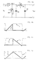
- prior power modules, or DC-to-DC converters have taken a number of forms, including that of the buck converter 20 of Fig. 2a. In Fig.
- a conventional buck converter, or current step-up power converter 20 utilizes an FET 21 for the series switch and a diode 22 for the flywheel rectifier.
- the FET 21 is turned on, impressing the input voltage, less the output voltage, across an inductor 23. Placing this voltage across the inductor causes the current in the inductor to increase, charging an output capacitor 24 while also delivering current to any load connected in parallel with the capacitor.
- Switching loss occurs when the FET 21 is turned on and off because of the finite time required for the current to start and stop flowing. As the FET is turned on, current flowing through the device causes the voltage on node 1 to rise, producing dissipation equal to the instantaneous product of current and voltage at the FET over the time interval required for turn on. Similarly, when the FET 21 is turned off, the simultaneous presence of voltage and current produces substantial dissipation. In the past, the diode 22 has been replaced with an additional FET (having an orientation as shown for the FET 32 in Fig. 3a). This improves efficiency in the converter. As earlier discussed, timing of FET turn on and turn off becomes critical in a two FET configuration. As also earlier discussed, it would be desirable to increase the frequency of operation of a standard converter such as the converter 20 in order to reduce the size of the reactive components in the converter. However, in increasing frequency, both switching loss and critical timing requirements become more difficult to deal with.
- a buck converter 30 configured in accordance with certain aspects of the invention includes a series switch FET 31 and a flywheel FET 32 connected at a node, designated node 1, with one terminal of an inductor 33.
- An output capacitor 34 is provided at the output of the converter 30, and a capacitor 36 is also provided in parallel with the flywheel FET 32.
- the FET's 31 and 32 are power MOSFET's including internal diodes.
- the FET 31 is a p-channel MOSFET and the FET 32 is an n-channel MOSFET.
- the source of the FET 31 is at the converter input and the drain of the FET 31 is connected to node 1, which is connected to the drain of the FET 32 and one terminal of the inductor 33.
- the source of the FET 32 is connected to circuit common, or ground.
- the gates of the FET's are coupled to a suitable control circuit as shall be described in more detail hereinafter.
- Each FET 31, 32 includes an internal diode, with the internal diode of the FET 31 poled to conduct current from node 1 toward the input, and the internal diode of the FET 32 poled to conduct current from circuit common to node 1.
- Each FET includes a parasitic capacitance, and due to the low impedance of the voltage source input, the capacitances of the FET's 31 and 32 are effectively connected in parallel between node 1 and circuit common.
- a physical capacitor 36 is not required, as the FET parasitic capacitances are of sufficient size to support the voltage at node 1 during turn-off of each of the FET's.
- the discrete capacitor 36 is omitted.
- the inductor 33 is selected to be of a value to insure that the inductor current polarity reverses during each normal cycle of operation (each cycle of turn-on and turn-off of the series FET 31). Insuring reversal of the inductor current requires not only the selection of the inductance value, but also (a) the operation of the converter with a peak forward inductor current that is not too large relative to the size of the output voltage and (b) the provision of a suitably long off-time for the series FET.
- the output voltage must be greater than or equal to the product of (a) the inductance of the inductor 33 and (b) the value of the peak inductor current (the inductor current when the series FET is turned off), divided by the length of the off-time of the series FET 31.
- a typical operating cycle for the converter 30 begins with the turn-off of the FET 31, after which the node 1 voltage falls until it reaches zero, as the inductor 33 draws current first from the capacitor 36 and then through the internal diode of the FET 32.
- the flywheel FET 32 is then turned on with zero switching loss since the voltage across it is zero at the time of turn-on.
- the flywheel FET 32 is not turned off until the direction of current flow in the inductor 33 has reversed, with current flow through the flywheel FET.
- the capacitor 36 holds the voltage at node 1 near zero during the turn off interval, after which the (now-reversed) current through the inductor 33 drives the node 1 voltage up to the level of the input voltage.
- flywheel FET is turned off and its internal diode is non-conductive since it is reverse biased.
- the series FET 31 is then turned on with substantially no voltage across the FET, so that there are substantially no turn-on losses. The cycle then repeats.
- the turn-on and turn-off of both the series FET 31 and the flywheel FET 32 occur with nearly zero volts across the FET's. Also, there is an inherent, desirable dead time between the turn-off of one FET and the turn-on of the other.
- the turn-on of the FET 31 occurs after the inductor current has reversed and taken node 1 to the level of VIN, and the turn-on of FET 32 occurs when the inductor current has taken node 1 low after the series FET 31 has been turned off.
- the turn-on timing of the FET's is less critical (allowing dead time) because stored charge in the FET internal diodes has the FET on-time to recombine if turn-on is late. That is, when each FET is turned on, the internal diode of the other FET is reverse biased and non-conductive so that energy is not expended in neutralizing the stored charge associated with the device forward voltage drop. Switch through (simultaneous FET conduction) will not result unless turn-on occurs prior to the normal transition dead time. Overall conversion efficiency and ease of control for the converter is therefore improved, and operation at high frequencies is permitted.
- a boost converter configured in accordance with the invention includes FET's 231 and 232 interconnected at node 1 and an inductor 233 connected between the input voltage VIN and node 1.
- a capacitor 234 is connected across the output VOUT, and a capacitor 236 is connected in parallel with the FET 232.
- a typical operating cycle begins with the turn-off of the FET 232, after which the voltage at node 1 rises to the level of VOUT as current in the inductor 233 charges the capacitor 236.
- the FET 231 is then turned on with zero switching loss, since the voltage across it is zero.
- the turn-off of the FET 231 does not occur until the direction of current flow in inductor 233 has reversed.
- the current in the inductor 233 draws charge from the capacitor 236 until the voltage on node 1 is zero, after which the cycle repeats. It should be noted that the turn-on and turn-off of the FET's 231 and 232 occur at zero voltage since the capacitor 236 holds the node 1 voltage almost constant while switching occurs. Operation and advantages are similar to those previously described for the buck converter of Fig. 3.
- the invention is embodied in a buck-boost converter which includes FET's 241 and 242, interconnected at node 1, to which is also connected an inductor 243.
- a capacitor 244 is coupled across the output VOUT, and a capacitor 246 is coupled across the inductor 243.
- a typical operating cycle of the converter begins with the turn-off of the FET 241. After the turn-off of the FET 241, the voltage between node 1 and ground falls to the level of VOUT as current in the inductor 243 discharges the capacitor 246.
- the FET 242 is then turned on with zero switching loss, since the voltage across it is zero.
- Turn-off of the FET 242 does not occur until the direction of current flow in the inductor 243 has reversed.
- the current in the inductor 243 charges the capacitor 246 until the voltage at node 1 is equal to VIN, after which the cycle repeats.
- turn-on and turn-off of the FET's 241 and 242 occur at zero voltage since the capacitor 246 holds the node 1 voltage almost constant while switching occurs.
- the operation and advantages of the buck-boost converter are similar to those previously described for the other converter topologies.
- a control circuit is provided for controlling the on- and off-times of the two FET's 31 and 32.
- Conventional control circuits for DC-to-DC converters usually provide output voltage regulation in one of three ways.
- constant frequency pulse width modulation the operating frequency is held constant while on-time of the series switch is varied to compensate for variations in input voltage and load.
- constant frequency peak current control the operating frequency is held constant while the maximum amplitude of the current in the series switch is varied to compensate for variations in load. Compensation for input voltage variations is inherent in the peak current control.
- constant on-time, variable frequency control the series switch on-time is held constant and off-time is varied to compensate for variations in load and input voltage.
- the converter circuit 30 it is advantageous to provide a control circuit which is independent of time constraints such as constant frequency or constant on-time. It has been found that the use of a control circuit which maintains a constant peak-to-peak current through the inductor 33 provides the requisite regulation and is particularly suited to the converter 30, which has a requirement that the inductor current reverse on each cycle of operation.
- a control circuit To produce output voltage regulation and constant peak-to-peak current, a control circuit must implement two timing equations.
- L is the inductance value of the inductor 33
- IP-P is the peak to peak value of the inductor current.
- VIN is the input voltage
- VOUT is the output voltage.
- a DC to DC converter 30 ⁇ (which is the same as the converter 30 of Fig. 3 with the addition of drive circuitry for the FET's) includes a drive circuit 37 for the FET 31 and a drive circuit 38 for the FET 32.
- These drive circuits receive control signals from the control circuit illustrated in Fig. 7 in order to control the conduction times of the FET's 31, 32.
- the connections of the control signals to the drive circuits are shown by the letter designations A and B in the schematic of Fig. 7 and the corresponding designations in Fig. 6.
- a control circuit 40 for the converter 30 ⁇ of Fig. 6 includes a capacitor 41 which is charged and discharged to simulate the peak-to-peak current flow through the inductor 33 in the converter. Just as the change in current per unit time through the inductor is proportional to the voltage across the inductor, the change in voltage on the capacitor is proportional to the current into the capacitor.
- a charging circuit 42 charges the capacitor 41 with a current during substantially the same time interval that the series FET 31 is turned on in the converter circuit 30 ⁇ .
- the voltage across the inductor 33 is equal to the difference between the input voltage and the output voltage of the converter.
- the charging circuit 42 provides a charging current to the capacitor 41 which is proportional to the difference between the input and output voltages on the converter. Therefore, since the time intervals are substantially the same and the charging current for the capacitor 41 is proportional to the voltage applied to the inductor 33, the voltage change on the capacitor 41 in the control circuit is substantially proportional to the current change in the inductor 33 in the inverter.
- a discharge circuit 43 in the control circuit 40 provides a discharge current (to discharge the capacitor 41) which in steady state is proportional to the converter output voltage during this interval.
- the discharge circuit 43 discharges the capacitor 41 over substantially the same time interval as that during which the inductor 33 is connected across the output voltage, and since the discharge current is proportional to the converter output voltage, the reduction in voltage on the capacitor 41 is proportional to the reduction in current through the inductor 33 in the converter.
- the voltage excursions of the capacitor 41 are compared to a reference by a comparator 44, the inverted and non-inverted outputs of which are coupled to the drive circuits 38, 37, respectively, in the converter 30 ⁇ .
- the non-inverted output (A) of the comparator 44 goes low and the output of the drive circuit 37 provides a positive signal to the gate of the FET 31, turning off the series switch, ending the current rise in the inductor 33 for that cycle.
- the inverted output (B) of the comparator 44 goes high, and the drive circuit 38 provides a positive signal to the flywheel FET 32, turning on the FET.
- the drive circuit 38 provides a delay prior to turning on the FET 32, as shall be described in more detail hereinafter.
- the comparator 44 changes state, with the drive circuit 38 turning off the flywheel FET 32 and the drive circuit 37 turning on the FET 31, after a suitable delay.
- a resistance divider made up of resistors 46, 47 and 48 is connected across the capacitor 41.
- the inverting input of the comparator 44 is connected to the junction between the resistors 46 and 47, and the non-inverting input of the comparator 44 is connected to a positive voltage reference produced by a voltage reference circuit 49.
- the voltage at the inverting input of the comparator 44 is lower than the reference voltage, and the non-inverted output of the comparator is at a logic high.
- This logic high is coupled through a resistor 51 to the base of a transistor 52, saturating the transistor and shorting out the resistor 48 in the resistance string. Therefore, the voltage at the junction between the resistor 46 and the resistor 47 is lower than the reference voltage and increasing as the capacitor 41 charges.
- the charging circuit 42 is turned on and off by saturating and turning off a transistor 53 in the charging circuit.
- the non-inverted output of the comparator 44 (at a logic high) is coupled through a resistor 54 to the base of the transistor 53, saturating the transistor and activating the charging circuit.
- a transistor 56 in the discharge circuit 43 is turned off, so that the discharge circuit does not discharge the capacitor 41.
- the inverted output of the comparator 44 is coupled through a resistor 57 to the base of the transistor 56, which (during the charging interval) is turned off by the logic low on the inverted output of the comparator.
- the charging circuit 42 produces a current (to charge the capacitor 41) which is proportional to the difference between the input and output voltages of the inverter circuit 30 ⁇ .
- This current flows through a transistor 58 from a voltage supply VCC.
- the transistor 58 is connected at the base and emitter to a diode 59 (which is preferably the base emitter junction of an identical transistor).
- the transistor 58 and the diode 59 are interconnected in the form of a "current mirror", and the current through the transistor 58 is identical to that flowing through the diode 59.
- the current through the diode 59 is established by the current through a transistor 60 and a resistor 67 connected in series with the diode 59 and the transistor 53.
- This current level is in turn established by an operational amplifier 68 in cooperation with resistors 61-66 to be proportional to the difference between the input and output voltages of the converter 30 ⁇ .
- the resistors 61-66 are chosen to yield a voltage at the emitter of the transistor 60 that is proportional to the difference between the converter input and output voltages.
- the resistor 67 converts the voltage at the emitter of the transistor 60 into a current that is, as described earlier, mirrored into the collector of the transistor 58 to charge the capacitor 41.
- the resistor 61 is 93K ohms
- the resistor 62 is 5K ohms
- the resistor 63 is 8.57K ohms
- the resistor 64 is 1K ohms
- the resistor 65 is 20K ohms
- the resistor 66 is 20K ohms
- the resistor 67 is 1.11K ohms.
- the voltage produced at the emitter of the transistor 60 in this configuration is about 0.1 times the difference between the input and output voltages of the converter 30 ⁇ .
- the charging current supplied to the capacitor 41 through the transistor 58 causes the voltage across the capacitor to rise until the voltage at the inverting input of the comparator 44 exceeds the reference voltage VREF.
- the comparator 44 then changes state, and the transistors 52 and 53 are turned off.
- the charging current ceases, and the voltage at the junction between the resistors 46 and 47 rises, since the resistor 48 is now effectively in series with the resistors 46 and 47, raising the threshold voltage for the comparator.
- the transistor 56 in the discharge circuit 43 is turned on since the inverted output of the comparator 44 is now high, while the non-inverted output of the comparator is low. Discharge current is now permitted to flow through a transistor 69 and a resistor 71 connected in series with the transistor 56.
- the comparator 44 outputs again change state, turning off the transistor 56 and turning on the transistors 52 and 53 to repeat the cycle.
- the level of the discharge current in the transistor 69 is set by the resistor 71 and an error voltage applied to the base of the transistor 69.
- This error voltage is proportional to the difference between the reference voltage VREF and a portion of the output voltage (of the inverter 30 ⁇ ) determined by resistors 72 and 73 connected in the form of a resistance divider between VOUT and circuit common, or ground.
- the divided down VOUT is coupled to the inverting input of an operational amplifier 74, whose non-inverting input is connected to the voltage reference VREF.
- a feedback network containing an impedance Z is provided for stability.
- the signal A from the non-inverted output of the comparator 44 is used to determine the on time of the series pass device (series FET 31) in the converter circuit 30 ⁇ . Since the signal A is high while the capacitor 41 is being charged to a set voltage by a current proportional to VIN - VOUT, the FET 31 will have an on time proportional to VIN - VOUT as is required.
- the signal B from the inverted output of the comparator 44 is used to determine the on time of the flywheel FET 32. This signal is high, turning on the FET 32, during the time that the capacitor 41 is being discharged by the transistor 69 in the discharge circuit 43.
- the operational amplifier 74 and surrounding circuitry adjust the current in the transistor 69 (over a number of cycles of operation) so that the non-inverting and inverting inputs of the operational amplifier 74 are at almost the same potential, in order to insure producing the desired output voltage level at VOUT of the converter 30 ⁇ . For example, if VOUT rises, the voltage at the inverting input to the operational amplifier 74 increases and thus the output of the amplifier goes down.
- a buck converter 30 ⁇ substantially the same as that shown in Fig. 3, includes additional circuitry to provide current limiting.
- the inductor current is substantially a triangular waveform as shown in Fig. 3d.
- the effective output current of the converter is one-half the sum of the maximum and minimum inductor currents.
- the minimum inductor current occurs when the flywheel FET 32 turns off, and the maximum current occurs when the series FET 31 turns off. Since peak-to-peak inductor current is maintained constant, the effective output current may be held below a given value by holding either the minimum or maximum current below a defined level. The minimum current may be held below a given level by sensing current in the flywheel FET 32 and not permitting the FET 32 to turn off until the current has fallen to the selected minimum value. If the minimum current is selected to be zero, it is sufficient to simply sense the voltage across the flywheel FET 32, keeping this device on until the polarity of the voltage across it reverses. The current limit set point will be independent of the on-state resistance of the FET 32 since only the polarity of the signal is sensed.
- Fig. 8 illustrates how such a current limit concept can be implemented.
- This control of the flywheel FET 32 is represented in Fig. 8 by the coupling of a signal from the control circuit to the reset input of a flip-flop 86 to effect the removal of the gate drive from the flywheel 32.
- the flip-flop 86 When the flip-flop 86 is reset, its Q output goes low, and this low is coupled to a driver 84, whose output (the gate drive for the flywheel 32) goes low, turning off the FET 32.
- the current limit circuitry of Fig. 8 functions to insure that the current in the flywheel FET 32 (and in the inductor 33) has reversed before the control circuit is permitted to remove the gate drive from the FET 32.
- the current limit circuitry includes an FET 81 connected in parallel with the flywheel FET 32 and a resistor 83 in series with the FET 81. When the flywheel FET 32 is conductive, the FET 81 is saturated, providing a low impedance path for the voltage across the FET 32 to the inverting input of a comparator 82. This permits accurate sensing of the voltage across the flywheel FET 32.
- the resistor 83 in series with the FET 81 has a relatively high resistance, and substantially the entire voltage across the FET 32 is coupled to the comparator 82 when the FET 81 is saturated.
- the FET 81 operates in the cut-off region, protecting the comparator input from damage due to excessive voltage, while allowing only a small current flow through the sensing circuit.
- the non-inverting input to the comparator 82 is at a lower voltage than the inverting input, and the output of the comparator 82 is low. This low, coupled through a delay circuit 85 and the AND gate 87 to the reset input of the flip-flop 86, prevents the flip-flop from being reset and thus maintains the drive to the gate of the flywheel FET 32.
- the voltage across the flywheel FET 32 changes polarity, and the output of the comparator 82 goes high.
- This high output from the comparator 82 is coupled to a delay circuit 85, the output of which goes high after a delay which is proportional to the magnitude of the output voltage.
- the reason for the delay is to allow the reverse current through the inductor 33 to rise to a sufficient level to insure that once the flywheel FET 32 is turned off, the node 1 voltage will rise to the level of VIN.
- the time required for the reverse current through the inductor 33 to reach the necessary level is dependent upon the magnitude of VOUT, and the delay circuit 85 takes this into account in providing the necessary delay interval for the reverse current to build in the inductor 33.
- the output of the delay circuit 85 goes high, and this high is one input to the AND gate 87.
- the control circuit determines when the FET 32 is turned off.
- the input to the AND gate 87 from the control circuit goes high prior to the time that the output of the delay circuit 85 goes high. Therefore, in current limit mode, the comparator 82 and the delay circuit 85 control the timing of the turn-off of the flywheel FET 32.
- the signal from the control circuit or the output of the delay circuit 85 is the first to go to a logic high, once both of these signals are high, the output of the AND gate 87 goes high, resetting the flip-flop 86 and removing the drive signal from the driver 84 from the flywheel FET 32. This turns off the FET 32, permitting voltage to build across the flywheel FET 32 at node 1.
- the current limit circuit shown in Fig. 8 is advantageous relative to prior current limit approaches in that a series sensing element in series with the FET 31 is not required. This eliminates the need for additional high-current carrying components and permits current limit sensing to be done with respect to circuit common, or the negative rail, simplifying the control circuitry.
- a converter 30′′′ similar to that of Fig. 3 includes a new over-voltage protection circuit. This circuit does not require an additional high-current device to shunt the output as in prior systems.
- a voltage divider made up of a resistor 91 and a resistor 92 is coupled across the converter output. The voltage at the junction between the resistors 91 and 92 is connected to the non-inverting input of a comparator 94, whose inverting input is connected to a voltage reference 93. If the output voltage of the converter rises above a threshold level, the voltage at the non-inverting input of the comparator exceeds the reference voltage, and the output of the comparator 94 goes high.
- a high output from the comparator 94 sets a latch 96, with the output of the latch high.
- the output of the latch is one input to an OR gate 97. If the output of the latch 96 goes high, the output of the OR gate goes high, holding on the flywheel FET 32.
- the control signals for the FET 32 are provided from a control circuit through the OR gate 97, with the input to the OR gate from the latch 96 merely remaining at a logic low.
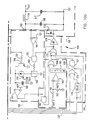
- a buck regulator 100 including the various aspects of the invention earlier described includes a power portion 101, a control circuit 102, FET drive circuits 103, 104, a current limit circuit 105, an over-voltage protection circuit 106, a node monitoring circuit 107, and input circuitry 108 for controlling turn-on and turn-off of the regulator.
- a series switch FET 111 is coupled between the input DC voltage VIN and a node 112 to which a flywheel FET 113 and an inductor 114 are also coupled.
- the other side of the inductor 114 is connected to the output voltage terminal VOUT of the regulator, and the other side of the flywheel FET 113 is connected to circuit common, or ground.
- An input capacitor 116 is connected between the input and ground, and an output capacitor 117 is connected between the output and ground.
- a capacitor 118 is connected to the node 112 to support the node voltage during turn off of the FET's 111 and 113. As earlier discussed, the capacitor 118 may be omitted in many cases, if the parasitic capacitances of the two FET's are sufficiently high.
- the power portion 101 of the regulator 100 operates in the same fashion as earlier described for the circuit of Fig. 3.
- a control circuit 102 emulates the peak-to-peak current through the inductor 114, utilizing the voltage on a capacitor 121.
- the control circuit 102 operates in a similar fashion to the control circuit shown in Fig. 7. In the control circuit 102, certain elements of the circuit have been shown diagrammatically, as is the case in certain other areas of the regulator circuit of Fig. 10.
- the voltage is rising on the capacitor 121 in the control circuit 102.
- the charging current to increase the voltage on the capacitor 121 is provided from a current source 122, which produces a current proportional to the difference between the input and output voltages of the power portion of the circuit.
- a switch 123 is closed by a logic high output 124 from an AND gate 126.
- a comparator 127 compares a fraction of the capacitor voltage to a reference voltage. The reference voltage is connected to the non-inverting input of the comparator 127.
- the capacitor voltage is divided down by a resistive divider including resistors 128, 129 and 131.
- a resistive divider including resistors 128, 129 and 131.
- the capacitor 121 As the capacitor 121 is charging, its divided-down voltage is less than the reference voltage connected to the comparator 127, and the non-inverted output 132 of the comparator 127 is at a logic high.
- This logic high is coupled through a resistor 133 to a transistor 134, which is turned on and shunts the resistor 131 in the resistance divider string connected across the capacitor 121. This results in a lower voltage being coupled to the inverting input of the comparator 127 during the charging cycle.
- the transistor 134 is turned off during the discharge cycle, the voltage coupled from the divider string to the inverting input of the comparator 127 is higher than the reference and moves downwardly as the capacitor 121 is discharged.
- the output 132 of the comparator 127 is also connected as one input to the AND gate 126, which controls the switch 123. Therefore, during the time that the capacitor 121 is charging, the AND gate 126 is enabled to produce a logic high output 124 when a suitable high output is obtained from the node monitoring circuit 107, as shall be described.
- a negative gate signal must be provided to the FET.
- the three inputs to an AND gate 137 in the FET drive circuit 103 must be at a logic high.
- a first input to the AND gate 137 is supplied from the non-inverted output 132 of the comparator 127, which during charging of the capacitor 121 and conduction of the series FET 111 is at a logic high.
- a second input to the AND gate 137 is supplied from an AND gate (having one inverting input) 138, the output of which is normally high when the regulator is turned on and not operating in the current limit mode.
- the third input to the AND gate 137 is the output of an OR gate 139, also in the drive circuit 103.
- the OR gate 139 has one input coupled through a delay circuit 141 to the non-inverted output 132 of the comparator 127. During start up, as the capacitor 121 is charged and discharged, the delay circuit 141 will provide an input to the OR gate 139 to begin operation of the FET drive, even in the absence of a signal at the other input to the OR gate 139.
- the other input to the OR gate 139 is from a comparator 142 in the node monitoring circuit 107.
- the non-inverted output 143 of the comparator 142 is coupled to both the second input of the OR gate 139 and the second input to the AND gate 126. Therefore, during normal operation of the regulator 100, with the series FET 111 conducting, and the capacitor 121 in the control circuit charging, the output 143 of the comparator 142 must be at a logic high.
- This logic high together with the other logic high inputs to the AND gate 126, provides a logic high output 124 of the AND gate 126, closing the switch 123 so that the current source 122 can charge the capacitor 121 in the control circuit.
- the non-inverted output 143 of the comparator 142 also produces a logic high at the output of the OR gate 139 which, together with the other two logic high inputs to the AND gate 137, produces a logic high at the output of the AND gate 137.
- This logic high at the output of the AND gate 137 is coupled to an inverting driver 144.
- the output of the driver 144 is therefore a logic low, which turns on the series FET 111.
- the function of the node monitoring circuit 107 is to insure that the voltage at the node 112 in the power portion of the regulator has reached a suitable level for turn on of each of the FET's 111, 113 at the requisite times. In other words, although the control circuit 102 may turn off one FET and enable the turn on of the other FET, the second FET will not be turned on until the node monitoring circuit 107 indicates that the voltage at the node 112 is at a suitable level.
- the circuit 107 includes a resistance divider made up of resistors 146 and 147 which divide down the node voltage.
- the divided down node voltage, at the junction 148 between the two resistors, is connected to the non-inverting input of the comparator 142.
- the inverting input is connected to a reference voltage.
- the comparator 142 includes a certain amount of hysteresis, so that the outputs of the comparator change state when the voltage at the node 112 reaches approximately the value of the input voltage and also when the voltage at the node 112 reaches approximately zero.
- the comparator 142 Prior to the time that the series FET 111 is turned on, the voltage rises at the node 112 due to the current reversal in the inductor 114. When this node voltage has risen to the level of the input voltage, the comparator 142 changes state with its non-inverted output 143 going to a logic high, at which it remains during conduction of the series FET 111. The outputs of the comparator 142 do not change until the voltage at the node 112 falls to zero, which does not occur until after the series FET 111 has been turned off.
- the non-inverted output 143 of the comparator 142 remains at a logic high, so that all three inputs to the AND gate 137 are a logic high, producing the appropriate gating signal to the FET 111, keeping it turned on.
- the comparator 142 with hysteresis can be replaced by two comparators if desired, one of which compares the voltage at the node 112 to a high reference and one of which compares the voltage at the node to a low reference.
- the voltage at the inverting input of the comparator 127 reaches the level of the reference input to the comparator, and the comparator outputs 132, 154 change state.
- the non-inverted output 132 of the comparator goes low, so that the output of the AND gate 126 goes low, opening the switch 123 and stopping the flow of charging current into the capacitor 121.
- the now-low output 132 from the comparator 127 also causes the output of the AND gate 137 to go low, taking the output of the inverting driver 144 high, turning off the series FET 111.
- the inverted output 154 of the comparator 127 goes high, providing a logic high input to the AND gate 153, to enable the discharge circuit for the capacitor 121.
- the inverted output 154 of the comparator 127 is also coupled as one input to an AND gate 157 in the driver circuit 104 for the flywheel FET 113.
- a second input 158 to the AND gate 157 is coupled from the turn on control line 171, and is normally high when the regulator is on.
- the third input to the AND gate 157 which is now enabled due to the logic high state of the inverted output 154 of the comparator 127, is from the inverted output 156 of the comparator 142.
- both the inductor 114 current and the capacitor 121 voltage will have rounded, or flattened, peaks. As will become apparent, this occurs at the turn off of each device, so that the waveforms of the inductor 114 current and the capacitor 121 voltage are triangular, with flattened upper and lower peaks.
- the non-inverting input to the comparator 142 in the node monitoring circuit 107 falls below the reference value, and the comparator 142 non-inverted output 143 goes low and the inverted output 156 goes high.
- the logic low on the output 143 is coupled to the AND gate 126 which controls the switch 123 for charging the capacitor 121; but this low input to the AND gate 126 has no effect at this time since the other input to the AND gate is already at a logic low due to the previous change in state of the comparator 127.
- the now-high inverted output 156 of the comparator 142 does have an effect on the control circuit and the power circuit.
- the output 156 is one input to the AND gate 153 in the control circuit 102.
- the other input to the AND gate 153 has previously gone high due to the change in state of the comparator 127. Therefore, once the output 156 from the comparator 142 goes high, the output of the AND gate 153 goes high, closing the switch 152 and permitting discharge of the capacitor 121 through the transistor 151 and a series resistor 161.
- the level of conductance of the transistor 151 is controlled by an amplifier 162 in a manner to maintain the output voltage of the regulator at a desired level, proportional to a reference voltage 163.
- the reference voltage is coupled through a resistor 164 to the non-inverting input of an amplifier 162.
- the regulator output voltage is coupled through a resistor 166 to the inverting input of the amplifier 162.
- a feedback capacitor 167 and resistor 168 provide a stable feedback loop for the amplifier 162.
- the discharge circuitry for the capacitor 121 also includes "soft start" circuitry operative when the regulator is turned on.
- an input control line 171 goes to a logic high, as shall be described in more detail hereinafter.
- This logic high is connected to an inverter 172, the output of which is coupled through a resistor 170 to the base of a transistor 173, which shunts the non-inverting input of the amplifier 162.
- This transistor 173, in cooperation with a capacitor 174 serves to provide a "soft start” for the control circuit.
- the capacitor 174 is charged by the voltage reference circuit 163 so that the full reference value does not appear at the reference input to the amplifier immediately upon turn on of the regulator. This has the effect of increasing the discharge interval for the capacitor 121 during start up of the regulator. This in turn permits the regulator to reach its normal operating level more slowly upon turn on.
- the OR gate 176 through which the logic high from the output 156 of the comparator 142 is coupled is provided to permit the connection of a delay circuit 179 for start-up operation.
- the delay circuit 179 functions in a manner analogous to the delay circuit 141, earlier described.
- the OR gate 177 through which the turn on signal from the comparator 142 is coupled, is provided to permit the flywheel FET 113 to be driven on by either the current limiting circuit 105 or the over voltage protection circuit 106, as shall be described hereinafter.
- the logic low at the output 154 of the comparator 127 opens the switch 152, ending discharge of the capacitor 121, and also takes the output of the AND gate 157 in the driver circuit 104 low, effecting turn-off of the flywheel FET 113.
- the logic high on the non-inverted output 132 of the comparator 127 is coupled to the AND gate 126 and to the AND gate 137, enabling both of these gates.
- the comparator 142 in the node monitoring circuit changes state.
- the non-inverted output 143 of the comparator goes high, coupling a logic high to the already enabled AND gates 126 and 137, so that the switch 123 is closed beginning the charging cycle for the capacitor 121 and the driver 144 is activated, turning on the series FET 111.
- the above-described cycle of operation then repeats.
- the over-voltage protection circuit 106 includes a resistive divider made up of resistors 181 and 182, with the junction between the resistors being connected to the non-inverting input of a comparator 183.
- the voltage at the non-inverting input to the comparator 183 which is proportional to the regulator output voltage VOUT, is compared to a reference value. If the regulator output voltage exceeds the reference value, the output of the comparator 183 goes high, and this logic high is coupled to a latch 185.
- the output of the latch 185 is latched high and coupled through an OR gate 184 and the OR gate 177 to the driver 178 for the flywheel FET 113, turning on and holding on the FET.
- the current limit circuit 105 functions to prevent turn-off of the flywheel FET 113 until the current through the FET has fallen below a specified value (that is, the reverse current through the coil 114 and the flywheel FET has exceeded a specified value).
- the time at which the current in the FET 113 passes through zero is determined by a comparator 191.
- the comparator 191 senses the voltage across the FET 113, and when this voltage goes above zero, indicative of current reversal, the output of the comparator 191 goes high.
- This output of the comparator 191 is coupled to an AND gate 192, which has a second input connected to the input to the driver 178 for the FET 113.
- the input to the AND gate 192 from the driver 178 input is high when the FET 113 is turned on.
- the output of the AND gate 192 goes high.
- the output of the AND gate 192 is coupled through a resistor 193 to a switch 194, and when the output of the AND gate goes high, the switch 194 is closed.
- a current source 195 is permitted to charge a capacitor 196.
- the current provided by the current source 195 is proportional to the level of the output voltage VOUT.
- the level of the voltage on the capacitor 196 is coupled to the inverting input of a comparator 197, whose non-inverting input is connected to a voltage reference.
- the output of the comparator 197 goes to a logic low.
- This low output of the comparator 197 is one input to an AND gate 198, whose other input is connected to the input of the FET driver 178. Therefore, when the FET 113 is turned on, and after the capacitor 196 in the current limit circuit 105 has charged sufficiently, the output of the AND gate 198 then goes low, and the output of the OR gate 184 goes low. This takes one of the inputs to the OR gate 177 low, and when its other input (from the control circuit 102) has gone low, this will deactivate the driver 178 and turn off the FET 113.
- the delay in turn off of the flywheel FET 113 caused by current in the current source 195 charging the capacitor 196 provides a time interval during which current increases in the flywheel FET. Since the current charging the capacitor 196 in the current limit circuit 105 is proportional to VOUT, as is the reverse current through the inductor 114, the current flowing into the flywheel FET 113 at the time of turn off will have a specified value during current limit operation which is independent of the actual value of VOUT. This insures that there will be sufficient energy in the inductor when the flywheel FET 113 is turned off to subsequently bring the voltage at the node 112 up to the level of VIN to permit lossless turn-on of the series FET 111.
- the input to the OR gate 177 from the OR gate 184 can go low upon the determination by the current limit circuit 105 that there is suitable reverse current flowing through the FET 113, without this turning off the FET 113. This is because the other input to the OR gate 177, produced from the control circuit 102, can remain high, which produces a high output of the OR gate 177 so that the driver 178 keeps the FET 113 turned on.
- the output 171 of an AND gate 202 serves as a turn on control line for the regulator 100.
- the line 171 is normally high when the regulator 100 is turned on.
- One input to the AND gate 202 is an on/off line, which is high when, for example, a power-on switch is activated.
- Two other inputs to the AND gate 202 must be high in order to activate the regulator 100. One of these insures that the input voltage is above a desired threshold, and the other insures that the temperature of the FET's is below a critical level.
- the input voltage VIN to the regulator is divided down by a resistance divider made up of a resistor 203 and a resistor 204.
- the divided down VIN is compared to a reference voltage by a comparator 206, which contains an amount of hysteresis, or which may be used in conjunction with a latch, with the output of the comparator 206 being normally high, but going low if the input voltage to the regulator is too low.
- the output of the comparator 206 is one input to the AND gate 202.
- a thermal shutdown circuit which produces the third input to the AND gate 202, includes a comparator 207, whose inverting input is connected to a resistance divider made up of resistors 208 and 209, coupled between a reference voltage and ground. The same reference voltage is also coupled through a resistor 211 and a diode 212 to ground.
- the diode 212 is physically located near the power FET's 111 and 113, and the diode characteristic is such that the voltage across the diode decreases as the temperature increases.
Abstract
Description
- This invention relates generally to power supplies and more particularly concerns DC-to-DC power converters.
- A common form of power converter is the DC-to-DC converter, which converts an input DC voltage to an output DC voltage having a desired value. Since the principal form of line power is AC, some type of AC-to-DC power supply is usually used to produce the requisite DC input voltage for the DC-to-DC converter. Where several different DC output voltages are required, several DC-to-DC converters, operating to produce the different output voltages, are connected in common to the same input DC voltage.
- There are a number of different topologies for DC-to-DC converters. In many cases, such a converter includes a semiconductor switch which is turned on and off to couple energy from the DC input to an inductor in the converter. This energy is transferred from the inductor to the DC output either during the on time or the off time of the switch, depending upon the converter topology. Common DC-to-DC converter topologies include the buck (or forward) converter, the buck-boost (or flyback) converter, and the boost converter topologies.
- As will be noted below with regard to an exemplary embodiment, the invention will find advantageous use in a buck, or forward, converter, but may also be used advantageously in other converter topologies.
- In a conventional buck converter, a semiconductor switch is connected between the DC supply input and an inductor, which is in turn connected to the output. The junction between the switch and the inductor is coupled to circuit common, or ground, by a diode (termed a "flywheel" diode), which is normally reverse biased and non-conductive when the semiconductor switch is closed. Ordinarily a capacitor is connected between the output and circuit common. A typical inductor in this form of converter has an inductance on the order of 100 microhenries, and a typical capacitor has a capacitance in the order of 500 microfarads.
- During normal operation of the conventional buck converter, the switch is closed, impressing the input voltage, less the output voltage, across the inductor. This causes the current in the inductor to increase, charging the output capacitor while also delivering current to any load connected at the output.
- When the switch is turned off, the voltage at the connection between the switch and the inductor falls until the diode becomes forward biased. Current then flows through the diode and the inductor with decreasing amplitude until the switch is again closed and the cycle repeated.
- In such prior art buck converters, it is advantageous to operate the converter at as high a frequency as possible, in order to reduce the size of the reactive components in the circuit. Typical prior art buck converters might operate at frequencies up to about twenty kilohertz. There have been upper limits to the operating frequency of prior art buck converters due to switching losses in the semiconductor switches in the converters.
- Switching losses occur when the series semiconductor switch in a buck converter is turned on and off because of the finite time required for the current to start and stop flowing in the device. As the switch is turned on, current flowing through the device causes the voltage at the junction between the device and the inductor to rise to the level of the input voltage, producing dissipation equal to the instantaneous product of the current through the device and the voltage across the device. Similarly, as the series switch is turned off, the simultaneous presence of a large voltage across the switch and a large current through the switch produces dissipation. These switching losses in the semiconductor switch increase with increasing frequency of operation since the number of switching excursions per unit time increases with frequency.
- In the past, power FET's have been used as series switches in buck converters in order to improve efficiency. The use of such a power FET is advantageous because it eliminates minority carrier storage time and permits faster switching. The FET drive circuitry is also more efficient than that for a bipolar transistor.
- A similar advantage in elimination of minority carriers is obtained if the diode in the converter is replaced with an FET. The use of an FET in place of the flywheel diode in prior buck converters has, however, called for critical timing of the FET turn-on and turn-off to avoid overlapping conduction of the series switch FET and the flywheel FET and to avoid "dead time" when neither device is conducting. Overlapping conduction of the FET series switch and the flywheel FET greatly increases dissipation in the circuit. Dead time causes parasitic diodes in the FET's to turn on, which in turn produces additional dissipation due to the presence of stored charge in one FET when the other FET is turned on.
- Not only does switching loss become more of a problem as operating frequency is increased, but the critical timing requirements for a two FET system also become more difficult to meet in order to avoid overlapping conduction or dead time as the time between switching events becomes shorter.
- Switching loss and loss due to timing errors are both directly proportional to frequency, as stated earlier, while the difficulty of maintaining tight tolerances on critical timing parameters to minimize timing errors increases as the switching period becomes shorter.
- It is the general aim of the present invention to permit significantly higher frequency operation of DC-to-DC converters of the foregoing type without the above-mentioned difficulties of large switching losses and critical timing requirements.
- This objective has been accomplished in accordance with certain principles of the invention by providing a DC-to-DC converter having an inductor whose inductance is sized to permit the current in the inductor to reverse direction during each operating cycle of the converter at a normal operating frequency. One form of the invention is a buck converter operable in the 300-800 kilohertz range, having a two microhenry inductor and an output capacitor of about 10 microfarads. In selecting the value of the inductance of the inductor, the output load voltage and the peak inductor current (that current present just prior to opening the series switch) are considered in order to insure that the inductor current will reverse during normal operation.
- In the new buck converter circuit, a series FET and a flywheel FET are employed, and a flywheel capacitor may be added in parallel with the flywheel FET. The value of the flywheel capacitance is chosen such that the voltage across the flywheel FET does not change appreciably during the time required for either FET to turn off. With this being true, the turn-off switching losses in each FET will be small, since the voltages across the devices will be maintained near the on-state value by the flywheel capacitance.
- In this exemplary buck converter, a suitable flywheel FET capacitance is in the order of 1000 picofarads. Since the circuit employs FET's rather than bipolar transistors, each of the switching devices has an inherent capacitance. This inherent capacitance is in the order of 500 picofarads. Since the impedance of the input voltage source to the converter is small, the capacitance of the series FET is substantially connected in parallel with the capacitance of the fly wheel FET, so that the desired 1000 picofarads can typically be obtained without the addition of an external capacitor.
- In operation of the new buck converter circuit, beginning at a time at which the series switch FET is conductive, current flows from the input voltage source through the series switch to a node at which the flywheel FET, the series switch FET and the inductor are connected. Current from the series switch FET flows through the inductor to the output, and the node is at substantially the same voltage level as the input. The series FET is then turned off, with the capacitance of the two FET's supporting the node voltage long enough so that there is substantially no voltage drop across the series switch during the turn off interval. After the series FET is turned off, the node voltage falls to zero as the inductor draws current from the capacitance. The flywheel FET is then turned on with substantially no switching loss, since it is connected between circuit common, or ground, and the zero voltage node, so there is no voltage across the flywheel FET when it is turned on.
- The flywheel FET is not turned off until the direction of current flow in the inductor has reversed, with current flowing from the output through the inductor. The node capacitance holds the node voltage near zero as the flywheel FET is turned off, after which current from the inductor drives the node voltage up to the level of the input voltage. The series FET is then turned on at a time when there is substantially zero voltage across it, thus minimizing turn on losses.
- Turn-on and turn-off of both FET's occur at near zero volts across the FET's. Voltage excursions at the node occur while only lossless reactive elements are conducting. Also, a dead time between turn-off of one FET and turn-on of the other occurs as the current in the inductor drives the voltage at the node either low or high. In the form of buck converter to be described in more detail hereinafter, the converter is controlled to provide output voltage regulation and hence to serve as a buck regulator. In order to do this, a control circuit is provided to turn the series and flywheel FET's on and off in a manner to maintain the peak-to-peak inductor current constant for variations in input voltage and load. The average value of this constant peak-to-peak inductor current is varied by the control circuit to provide output voltage regulation.
- In this exemplary system, with the peak-to-peak inductor current being maintained constant by the control circuit, the minimum value of the inductor current is held at or below a selected level, which in turn sets the maximum, or peak, inductor current. This provides current limiting in the event of a failure such as a short circuit across the output.
- Briefly, the control circuit functions to provide an on time for the series FET proportional to (a) the input voltage minus (b) the output voltage, so that the peak to peak current swing in the inductor is constant. The minimum, or lower peak, conductor current is held at or below a given level by sensing the current in the flywheel FET and not permitting this FET to turn off until the current has fallen to the selected level. Inherent in this operation is a variation in the frequency of operation of the converter, but within an acceptable range for normal operation of the converter.
- The exemplary buck regulator to be described hereinafter further includes a protection circuit for preventing an over-voltage condition, a condition in which the input voltage to the regulator appears at the regulator output. This protection circuit does not require an additional high current device to shunt the output, but instead turns on the flywheel FET in the event of a regulator output over-voltage condition.
- Other objects and advantages of the invention, and the manner of their implementation, will become apparent upon reading the following detailed description and upon reference to the drawings, in which:
-
- Fig. 1 is a schematic illustration of a power supply arrangement utilizing DC to DC converters in accordance with the present invention;
- Fig. 2 is a circuit diagram and illustrative waveforms for a prior art DC to DC buck converter;
- Fig. 3 is a circuit diagram and illustrative waveforms for a DC-to-DC buck converter in accordance with an aspect of the present invention;
- Fig. 4 is a circuit diagram and illustrative waveforms for a DC-to-DC boost converter in accordance with an aspect of the present invention;
- Fig. 5 is a circuit diagram and illustrative waveforms for a DC-to-DC buck-boost converter in accordance with an aspect of the present invention;
- Fig. 6 is a diagrammatic illustration of the converter of Fig. 3 showing additional elements of peak-to-peak current control circuitry;
- Fig. 7 is a circuit diagram of a peak-to-peak current control circuit for the buck converter of Fig. 3;
- Fig. 8 is a diagrammatic illustration of the buck converter of Fig. 3 together with current limit circuitry;
- Fig. 9 is a diagrammatic illustration of the buck converter of Fig. 3 together with output over-voltage protection circuitry; and
- Fig. 10 is a circuit diagram of an illustrative DC-to-DC buck converter including circuitry for peak-to-peak current control, current limiting, over-voltage protection and other control functions.
- While the invention is susceptible to various modifications and alternative forms, certain illustrative embodiments thereof have been shown by way of example in the drawings and will herein be described in detail. It should be understood that it is not intended to limit the invention to the particular forms disclosed, but the intention is to cover all modifications, equivalents, and alternatives falling within the spirit and scope of the invention, as defined by the appended claims.
- With initial reference to Fig. 1, a
power supply arrangement 10 includes a single output off-line switcher 11 which converts an AC input to a single level DC output. The output of the off-line switcher 11 is then coupled to a number ofpower modules outputs buck converter 20 of Fig. 2a. In Fig. 2a, a conventional buck converter, or current step-up power converter, 20 utilizes anFET 21 for the series switch and adiode 22 for the flywheel rectifier. During normal operation of this standard converter, theFET 21 is turned on, impressing the input voltage, less the output voltage, across aninductor 23. Placing this voltage across the inductor causes the current in the inductor to increase, charging anoutput capacitor 24 while also delivering current to any load connected in parallel with the capacitor. - When the
FET 21 is turned off, the voltage at node 1 (the connection point for theFET 21, thediode 22 and the inductor 23) falls until thediode 22 becomes forward biased. Current then flows through thediode 22 and theinductor 23 with decreasing amplitude until theFET 21 is again turned on and the cycle repeated. - Switching loss occurs when the
FET 21 is turned on and off because of the finite time required for the current to start and stop flowing. As the FET is turned on, current flowing through the device causes the voltage onnode 1 to rise, producing dissipation equal to the instantaneous product of current and voltage at the FET over the time interval required for turn on. Similarly, when theFET 21 is turned off, the simultaneous presence of voltage and current produces substantial dissipation. In the past, thediode 22 has been replaced with an additional FET (having an orientation as shown for theFET 32 in Fig. 3a). This improves efficiency in the converter. As earlier discussed, timing of FET turn on and turn off becomes critical in a two FET configuration. As also earlier discussed, it would be desirable to increase the frequency of operation of a standard converter such as theconverter 20 in order to reduce the size of the reactive components in the converter. However, in increasing frequency, both switching loss and critical timing requirements become more difficult to deal with. - Turning now to Fig. 3, a
buck converter 30 configured in accordance with certain aspects of the invention includes aseries switch FET 31 and aflywheel FET 32 connected at a node, designatednode 1, with one terminal of aninductor 33. Anoutput capacitor 34 is provided at the output of theconverter 30, and acapacitor 36 is also provided in parallel with theflywheel FET 32. The FET's 31 and 32 are power MOSFET's including internal diodes. TheFET 31 is a p-channel MOSFET and theFET 32 is an n-channel MOSFET. The source of theFET 31 is at the converter input and the drain of theFET 31 is connected tonode 1, which is connected to the drain of theFET 32 and one terminal of theinductor 33. The source of theFET 32 is connected to circuit common, or ground. The gates of the FET's are coupled to a suitable control circuit as shall be described in more detail hereinafter. - Each
FET FET 31 poled to conduct current fromnode 1 toward the input, and the internal diode of theFET 32 poled to conduct current from circuit common tonode 1. Each FET includes a parasitic capacitance, and due to the low impedance of the voltage source input, the capacitances of the FET's 31 and 32 are effectively connected in parallel betweennode 1 and circuit common. In many cases, aphysical capacitor 36 is not required, as the FET parasitic capacitances are of sufficient size to support the voltage atnode 1 during turn-off of each of the FET's. In subsequent illustrations of the converter of Fig. 3, thediscrete capacitor 36 is omitted. - In the
converter 30, theinductor 33 is selected to be of a value to insure that the inductor current polarity reverses during each normal cycle of operation (each cycle of turn-on and turn-off of the series FET 31). Insuring reversal of the inductor current requires not only the selection of the inductance value, but also (a) the operation of the converter with a peak forward inductor current that is not too large relative to the size of the output voltage and (b) the provision of a suitably long off-time for the series FET. To insure current reversal, the output voltage must be greater than or equal to the product of (a) the inductance of theinductor 33 and (b) the value of the peak inductor current (the inductor current when the series FET is turned off), divided by the length of the off-time of theseries FET 31. - A typical operating cycle for the
converter 30 begins with the turn-off of theFET 31, after which thenode 1 voltage falls until it reaches zero, as theinductor 33 draws current first from thecapacitor 36 and then through the internal diode of theFET 32. Theflywheel FET 32 is then turned on with zero switching loss since the voltage across it is zero at the time of turn-on. Theflywheel FET 32 is not turned off until the direction of current flow in theinductor 33 has reversed, with current flow through the flywheel FET. When the fly wheel FET is turned off, thecapacitor 36 holds the voltage atnode 1 near zero during the turn off interval, after which the (now-reversed) current through theinductor 33 drives thenode 1 voltage up to the level of the input voltage. Note that at this time the flywheel FET is turned off and its internal diode is non-conductive since it is reverse biased. Theseries FET 31 is then turned on with substantially no voltage across the FET, so that there are substantially no turn-on losses. The cycle then repeats. - It should be noted that the turn-on and turn-off of both the
series FET 31 and theflywheel FET 32 occur with nearly zero volts across the FET's. Also, there is an inherent, desirable dead time between the turn-off of one FET and the turn-on of the other. The turn-on of theFET 31 occurs after the inductor current has reversed and takennode 1 to the level of VIN, and the turn-on ofFET 32 occurs when the inductor current has takennode 1 low after theseries FET 31 has been turned off. - The turn-on timing of the FET's is less critical (allowing dead time) because stored charge in the FET internal diodes has the FET on-time to recombine if turn-on is late. That is, when each FET is turned on, the internal diode of the other FET is reverse biased and non-conductive so that energy is not expended in neutralizing the stored charge associated with the device forward voltage drop. Switch through (simultaneous FET conduction) will not result unless turn-on occurs prior to the normal transition dead time. Overall conversion efficiency and ease of control for the converter is therefore improved, and operation at high frequencies is permitted.
- While the presently preferred form of converter is a buck converter, the principles of the invention are applicable to other converter topologies such as the boost converter and buck-boost converter topologies. With reference, for example, to Fig. 4, a boost converter configured in accordance with the invention includes FET's 231 and 232 interconnected at
node 1 and aninductor 233 connected between the input voltage VIN andnode 1. Acapacitor 234 is connected across the output VOUT, and acapacitor 236 is connected in parallel with theFET 232. - A typical operating cycle begins with the turn-off of the
FET 232, after which the voltage atnode 1 rises to the level of VOUT as current in theinductor 233 charges thecapacitor 236. TheFET 231 is then turned on with zero switching loss, since the voltage across it is zero. The turn-off of theFET 231 does not occur until the direction of current flow ininductor 233 has reversed. After the turn-off of theFET 231, the current in theinductor 233 draws charge from thecapacitor 236 until the voltage onnode 1 is zero, after which the cycle repeats. It should be noted that the turn-on and turn-off of the FET's 231 and 232 occur at zero voltage since thecapacitor 236 holds thenode 1 voltage almost constant while switching occurs. Operation and advantages are similar to those previously described for the buck converter of Fig. 3. - With reference now to Fig. 5, the invention is embodied in a buck-boost converter which includes FET's 241 and 242, interconnected at
node 1, to which is also connected aninductor 243. Acapacitor 244 is coupled across the output VOUT, and acapacitor 246 is coupled across theinductor 243. A typical operating cycle of the converter begins with the turn-off of theFET 241. After the turn-off of theFET 241, the voltage betweennode 1 and ground falls to the level of VOUT as current in theinductor 243 discharges thecapacitor 246. TheFET 242 is then turned on with zero switching loss, since the voltage across it is zero. Turn-off of theFET 242 does not occur until the direction of current flow in theinductor 243 has reversed. After the turn-off of theFET 242, the current in theinductor 243 charges thecapacitor 246 until the voltage atnode 1 is equal to VIN, after which the cycle repeats. Again, it should be noted that turn-on and turn-off of the FET's 241 and 242 occur at zero voltage since thecapacitor 246 holds thenode 1 voltage almost constant while switching occurs. The operation and advantages of the buck-boost converter are similar to those previously described for the other converter topologies. - Returning to consideration of the buck converter of Fig. 3, in order to regulate the output of the
buck converter 30, a control circuit is provided for controlling the on- and off-times of the two FET's 31 and 32. - Conventional control circuits for DC-to-DC converters usually provide output voltage regulation in one of three ways. In constant frequency pulse width modulation, the operating frequency is held constant while on-time of the series switch is varied to compensate for variations in input voltage and load. In constant frequency peak current control, the operating frequency is held constant while the maximum amplitude of the current in the series switch is varied to compensate for variations in load. Compensation for input voltage variations is inherent in the peak current control. In constant on-time, variable frequency control, the series switch on-time is held constant and off-time is varied to compensate for variations in load and input voltage.
- In the
converter circuit 30, it is advantageous to provide a control circuit which is independent of time constraints such as constant frequency or constant on-time. It has been found that the use of a control circuit which maintains a constant peak-to-peak current through theinductor 33 provides the requisite regulation and is particularly suited to theconverter 30, which has a requirement that the inductor current reverse on each cycle of operation. - To produce output voltage regulation and constant peak-to-peak current, a control circuit must implement two timing equations. The on-time of the series switch, in this case the
series FET 31, is given by:
TON1 = (L)(IP-P)/(VIN - VOUT) (1)
In this expression L is the inductance value of theinductor 33, and IP-P is the peak to peak value of the inductor current. VIN is the input voltage, and VOUT is the output voltage. The on-time of the flywheel device, in this instance theflywheel FET 32, is given by:
TON2 = (L)(IP-P)/(VOUT) (2)
In Fig. 6 a DC to DC converter 30ʹ (which is the same as theconverter 30 of Fig. 3 with the addition of drive circuitry for the FET's) includes adrive circuit 37 for theFET 31 and adrive circuit 38 for theFET 32. These drive circuits, exemplary forms of which shall be described in more detail hereinafter, receive control signals from the control circuit illustrated in Fig. 7 in order to control the conduction times of the FET's 31, 32. The connections of the control signals to the drive circuits are shown by the letter designations A and B in the schematic of Fig. 7 and the corresponding designations in Fig. 6. - As shown in Fig. 7, a
control circuit 40 for the converter 30ʹ of Fig. 6 includes a capacitor 41 which is charged and discharged to simulate the peak-to-peak current flow through theinductor 33 in the converter. Just as the change in current per unit time through the inductor is proportional to the voltage across the inductor, the change in voltage on the capacitor is proportional to the current into the capacitor. - In the control circuit of Fig. 7, a charging
circuit 42 charges the capacitor 41 with a current during substantially the same time interval that theseries FET 31 is turned on in the converter circuit 30ʹ. In the converter circuit, during this time, the voltage across theinductor 33 is equal to the difference between the input voltage and the output voltage of the converter. In thecontrol circuit 40, the chargingcircuit 42 provides a charging current to the capacitor 41 which is proportional to the difference between the input and output voltages on the converter. Therefore, since the time intervals are substantially the same and the charging current for the capacitor 41 is proportional to the voltage applied to theinductor 33, the voltage change on the capacitor 41 in the control circuit is substantially proportional to the current change in theinductor 33 in the inverter. - During the time interval that the
series FET 31 is non-conductive and theflywheel FET 32 is conductive, the current in theinductor 33 decreases. During this interval, the voltage across the inductor is substantially equal to VOUT (applied in a reverse direction). Adischarge circuit 43 in thecontrol circuit 40 provides a discharge current (to discharge the capacitor 41) which in steady state is proportional to the converter output voltage during this interval. As in the case of the chargingcircuit 42, since thedischarge circuit 43 discharges the capacitor 41 over substantially the same time interval as that during which theinductor 33 is connected across the output voltage, and since the discharge current is proportional to the converter output voltage, the reduction in voltage on the capacitor 41 is proportional to the reduction in current through theinductor 33 in the converter. - In the
control circuit 40, the voltage excursions of the capacitor 41 are compared to a reference by acomparator 44, the inverted and non-inverted outputs of which are coupled to thedrive circuits - When the voltage on the capacitor 41 reaches its upper limit, the non-inverted output (A) of the
comparator 44 goes low and the output of thedrive circuit 37 provides a positive signal to the gate of theFET 31, turning off the series switch, ending the current rise in theinductor 33 for that cycle. At the same time, the inverted output (B) of thecomparator 44 goes high, and thedrive circuit 38 provides a positive signal to theflywheel FET 32, turning on the FET. In practice, thedrive circuit 38 provides a delay prior to turning on theFET 32, as shall be described in more detail hereinafter. In like fashion, when the voltage excursion of the voltage on the capacitor 41 reaches a low limit, thecomparator 44 changes state, with thedrive circuit 38 turning off theflywheel FET 32 and thedrive circuit 37 turning on theFET 31, after a suitable delay. - In the
control circuit 40, a resistance divider made up ofresistors comparator 44 is connected to the junction between theresistors comparator 44 is connected to a positive voltage reference produced by avoltage reference circuit 49. When the capacitor 41 is being charged by the chargingcircuit 42, the voltage at the inverting input of thecomparator 44 is lower than the reference voltage, and the non-inverted output of the comparator is at a logic high. This logic high is coupled through aresistor 51 to the base of a transistor 52, saturating the transistor and shorting out theresistor 48 in the resistance string. Therefore, the voltage at the junction between theresistor 46 and theresistor 47 is lower than the reference voltage and increasing as the capacitor 41 charges. - The charging
circuit 42 is turned on and off by saturating and turning off atransistor 53 in the charging circuit. During the charging interval, the non-inverted output of the comparator 44 (at a logic high) is coupled through aresistor 54 to the base of thetransistor 53, saturating the transistor and activating the charging circuit. During the charging interval, atransistor 56 in thedischarge circuit 43 is turned off, so that the discharge circuit does not discharge the capacitor 41. The inverted output of thecomparator 44 is coupled through aresistor 57 to the base of thetransistor 56, which (during the charging interval) is turned off by the logic low on the inverted output of the comparator. - The charging
circuit 42 produces a current (to charge the capacitor 41) which is proportional to the difference between the input and output voltages of the inverter circuit 30ʹ. This current flows through atransistor 58 from a voltage supply VCC. Thetransistor 58 is connected at the base and emitter to a diode 59 (which is preferably the base emitter junction of an identical transistor). Thetransistor 58 and thediode 59 are interconnected in the form of a "current mirror", and the current through thetransistor 58 is identical to that flowing through thediode 59. The current through thediode 59 is established by the current through atransistor 60 and aresistor 67 connected in series with thediode 59 and thetransistor 53. This current level is in turn established by anoperational amplifier 68 in cooperation with resistors 61-66 to be proportional to the difference between the input and output voltages of the converter 30ʹ. - The resistors 61-66 are chosen to yield a voltage at the emitter of the
transistor 60 that is proportional to the difference between the converter input and output voltages. When thetransistor 53 is turned on by thecomparator 44, theresistor 67 converts the voltage at the emitter of thetransistor 60 into a current that is, as described earlier, mirrored into the collector of thetransistor 58 to charge the capacitor 41. - In one form of charging
circuit 42, theresistor 61 is 93K ohms, theresistor 62 is 5K ohms, theresistor 63 is 8.57K ohms, theresistor 64 is 1K ohms, theresistor 65 is 20K ohms, theresistor 66 is 20K ohms, and theresistor 67 is 1.11K ohms. The voltage produced at the emitter of thetransistor 60 in this configuration is about 0.1 times the difference between the input and output voltages of the converter 30ʹ. - The charging current supplied to the capacitor 41 through the
transistor 58 causes the voltage across the capacitor to rise until the voltage at the inverting input of thecomparator 44 exceeds the reference voltage VREF. Thecomparator 44 then changes state, and thetransistors 52 and 53 are turned off. The charging current ceases, and the voltage at the junction between theresistors resistor 48 is now effectively in series with theresistors - At the same time, the
transistor 56 in thedischarge circuit 43 is turned on since the inverted output of thecomparator 44 is now high, while the non-inverted output of the comparator is low. Discharge current is now permitted to flow through atransistor 69 and aresistor 71 connected in series with thetransistor 56. When the voltage at the inverting input of thecomparator 44 falls below the reference voltage VREF, thecomparator 44 outputs again change state, turning off thetransistor 56 and turning on thetransistors 52 and 53 to repeat the cycle. - While the capacitor 41 is being discharged by the
discharge circuit 43, the level of the discharge current in thetransistor 69 is set by theresistor 71 and an error voltage applied to the base of thetransistor 69. This error voltage is proportional to the difference between the reference voltage VREF and a portion of the output voltage (of the inverter 30ʹ) determined byresistors operational amplifier 74, whose non-inverting input is connected to the voltage reference VREF. A feedback network containing an impedance Z is provided for stability. The operation of thecontrol circuit 40 to establish the proper conduction intervals for theFET 31 and theFET 32 shall now be described. - The signal A from the non-inverted output of the
comparator 44 is used to determine the on time of the series pass device (series FET 31) in the converter circuit 30ʹ. Since the signal A is high while the capacitor 41 is being charged to a set voltage by a current proportional to VIN - VOUT, theFET 31 will have an on time proportional to VIN - VOUT as is required. - The signal B from the inverted output of the
comparator 44 is used to determine the on time of theflywheel FET 32. This signal is high, turning on theFET 32, during the time that the capacitor 41 is being discharged by thetransistor 69 in thedischarge circuit 43. Theoperational amplifier 74 and surrounding circuitry adjust the current in the transistor 69 (over a number of cycles of operation) so that the non-inverting and inverting inputs of theoperational amplifier 74 are at almost the same potential, in order to insure producing the desired output voltage level at VOUT of the converter 30ʹ. For example, if VOUT rises, the voltage at the inverting input to theoperational amplifier 74 increases and thus the output of the amplifier goes down. This reduces the current through thetransistor 69 and theresistor 71 so that the capacitor 41 discharges more slowly. This decreases the duty cycle of the inverter 30ʹ (by increasing the off time of the series FET 31). This will in turn bring down the converter output voltage to its proper level, perhaps after a few cycles of operation. - Turning now to Fig. 8, a buck converter 30ʺ substantially the same as that shown in Fig. 3, includes additional circuitry to provide current limiting. When the converter is controlled by a control circuit to provide constant peak-to-peak current through the
inductor 33, the inductor current is substantially a triangular waveform as shown in Fig. 3d. With changes in the load on the output of the converter, the current waveform in effect shifts upward and downward to transfer more or less average current from the input to the output, as required. The effective output current of the converter is one-half the sum of the maximum and minimum inductor currents. - The minimum inductor current occurs when the
flywheel FET 32 turns off, and the maximum current occurs when theseries FET 31 turns off. Since peak-to-peak inductor current is maintained constant, the effective output current may be held below a given value by holding either the minimum or maximum current below a defined level. The minimum current may be held below a given level by sensing current in theflywheel FET 32 and not permitting theFET 32 to turn off until the current has fallen to the selected minimum value. If the minimum current is selected to be zero, it is sufficient to simply sense the voltage across theflywheel FET 32, keeping this device on until the polarity of the voltage across it reverses. The current limit set point will be independent of the on-state resistance of theFET 32 since only the polarity of the signal is sensed. - Fig. 8 illustrates how such a current limit concept can be implemented. During normal operation of the converter 30ʺ, toward the end of the conduction interval for the
flywheel FET 32, current reverses in theinductor 33 and flows in the direction of the current arrow I2 through theFET 32. Normally, the duration of this reverse current is established by the converter control circuit in order to establish the appropriate net forward current flow through theinductor 33 to provide the desired regulation of the output voltage VOUT. - This control of the
flywheel FET 32 is represented in Fig. 8 by the coupling of a signal from the control circuit to the reset input of a flip-flop 86 to effect the removal of the gate drive from theflywheel 32. When the flip-flop 86 is reset, its Q output goes low, and this low is coupled to adriver 84, whose output (the gate drive for the flywheel 32) goes low, turning off theFET 32. - The current limit circuitry of Fig. 8 functions to insure that the current in the flywheel FET 32 (and in the inductor 33) has reversed before the control circuit is permitted to remove the gate drive from the
FET 32. The current limit circuitry includes anFET 81 connected in parallel with theflywheel FET 32 and aresistor 83 in series with theFET 81. When theflywheel FET 32 is conductive, theFET 81 is saturated, providing a low impedance path for the voltage across theFET 32 to the inverting input of acomparator 82. This permits accurate sensing of the voltage across theflywheel FET 32. Theresistor 83 in series with theFET 81 has a relatively high resistance, and substantially the entire voltage across theFET 32 is coupled to thecomparator 82 when theFET 81 is saturated. When theflywheel FET 32 is non-conductive, theFET 81 operates in the cut-off region, protecting the comparator input from damage due to excessive voltage, while allowing only a small current flow through the sensing circuit. - Before the reversal of current in the
FET 32, the non-inverting input to thecomparator 82 is at a lower voltage than the inverting input, and the output of thecomparator 82 is low. This low, coupled through adelay circuit 85 and the ANDgate 87 to the reset input of the flip-flop 86, prevents the flip-flop from being reset and thus maintains the drive to the gate of theflywheel FET 32. - After the current in the
flywheel FET 32 has reversed, so that it is flowing in the direction of the current arrow I2, the voltage across theflywheel FET 32 changes polarity, and the output of thecomparator 82 goes high. This high output from thecomparator 82 is coupled to adelay circuit 85, the output of which goes high after a delay which is proportional to the magnitude of the output voltage. The reason for the delay is to allow the reverse current through theinductor 33 to rise to a sufficient level to insure that once theflywheel FET 32 is turned off, thenode 1 voltage will rise to the level of VIN. The time required for the reverse current through theinductor 33 to reach the necessary level is dependent upon the magnitude of VOUT, and thedelay circuit 85 takes this into account in providing the necessary delay interval for the reverse current to build in theinductor 33. - After this delay interval, the output of the
delay circuit 85 goes high, and this high is one input to the ANDgate 87. - During normal operation of the converter 30ʺ, the output of the
delay circuit 85 goes high before a logic high is coupled to the ANDgate 87 from the control circuit. Therefore, during normal operation, the control circuit determines when theFET 32 is turned off. However, during current limit mode, when the control circuit is attempting to couple more energy than is permitted from the input to the output of the converter, the input to the ANDgate 87 from the control circuit goes high prior to the time that the output of thedelay circuit 85 goes high. Therefore, in current limit mode, thecomparator 82 and thedelay circuit 85 control the timing of the turn-off of theflywheel FET 32. - Whether the signal from the control circuit or the output of the
delay circuit 85 is the first to go to a logic high, once both of these signals are high, the output of the ANDgate 87 goes high, resetting the flip-flop 86 and removing the drive signal from thedriver 84 from theflywheel FET 32. This turns off theFET 32, permitting voltage to build across theflywheel FET 32 atnode 1. - The current limit circuit shown in Fig. 8 is advantageous relative to prior current limit approaches in that a series sensing element in series with the
FET 31 is not required. This eliminates the need for additional high-current carrying components and permits current limit sensing to be done with respect to circuit common, or the negative rail, simplifying the control circuitry. - Failures in buck converters that cause the series pass device, such as the
series FET 31, to appear as a continuous low impedance can result in the input voltage of the converter appearing at the converter output. Since the value of this voltage may exceed the maximum voltage rating of devices connected to the output of the converter, a failure of this type can destroy many devices downstream from the converter, compounding the cost of the original failure. To prevent this from occurring, various protection circuits have been utilized. In one such circuit, the converter output voltage is sensed, and if it exceeds a selected threshold, an SCR connected in parallel with the output is gated on, impressing a low impedance across the output. A fuse is provided in series with the series pass device, and the ensuing surge of current when the SCR is turned on opens the fuse, removing input power from the converter. - In Fig. 9, a
converter 30‴ similar to that of Fig. 3 includes a new over-voltage protection circuit. This circuit does not require an additional high-current device to shunt the output as in prior systems. In Fig. 9, a voltage divider made up of aresistor 91 and aresistor 92 is coupled across the converter output. The voltage at the junction between theresistors comparator 94, whose inverting input is connected to avoltage reference 93. If the output voltage of the converter rises above a threshold level, the voltage at the non-inverting input of the comparator exceeds the reference voltage, and the output of thecomparator 94 goes high. A high output from thecomparator 94 sets alatch 96, with the output of the latch high. The output of the latch is one input to anOR gate 97. If the output of thelatch 96 goes high, the output of the OR gate goes high, holding on theflywheel FET 32. During normal operation of theconverter 30‴, the control signals for theFET 32 are provided from a control circuit through theOR gate 97, with the input to the OR gate from thelatch 96 merely remaining at a logic low. - If an over-voltage condition does arise, and the
FET 32 is held on by thelatch 96, when theseries FET 31 is turned on, the resulting current surge (as current flows through the FET's 31 and 32) opens a fuse 98 connected in series with theFET 31 at the converter input. Opening the fuse 98 removes the input power from the converter. - Turning now to Fig. 10, a
buck regulator 100 including the various aspects of the invention earlier described includes apower portion 101, acontrol circuit 102, FET drivecircuits 103, 104, acurrent limit circuit 105, anover-voltage protection circuit 106, anode monitoring circuit 107, andinput circuitry 108 for controlling turn-on and turn-off of the regulator. - In the
power portion 101 of the regulator, aseries switch FET 111 is coupled between the input DC voltage VIN and anode 112 to which aflywheel FET 113 and an inductor 114 are also coupled. The other side of the inductor 114 is connected to the output voltage terminal VOUT of the regulator, and the other side of theflywheel FET 113 is connected to circuit common, or ground. Aninput capacitor 116 is connected between the input and ground, and anoutput capacitor 117 is connected between the output and ground. These capacitors provide filtering to reduce ripple at the input and output. - A
capacitor 118 is connected to thenode 112 to support the node voltage during turn off of the FET's 111 and 113. As earlier discussed, thecapacitor 118 may be omitted in many cases, if the parasitic capacitances of the two FET's are sufficiently high. Thepower portion 101 of theregulator 100 operates in the same fashion as earlier described for the circuit of Fig. 3. - In order to provide the gate signals to turn the FET's 111 and 113 on and off at suitable times, a
control circuit 102 emulates the peak-to-peak current through the inductor 114, utilizing the voltage on acapacitor 121. Thecontrol circuit 102 operates in a similar fashion to the control circuit shown in Fig. 7. In thecontrol circuit 102, certain elements of the circuit have been shown diagrammatically, as is the case in certain other areas of the regulator circuit of Fig. 10. - Continuing with the description of the control circuit, starting from a time when the
series FET 111 is conducting, the voltage is rising on thecapacitor 121 in thecontrol circuit 102. The charging current to increase the voltage on thecapacitor 121 is provided from acurrent source 122, which produces a current proportional to the difference between the input and output voltages of the power portion of the circuit. During the time that thecapacitor 121 is charging, aswitch 123 is closed by a logichigh output 124 from an ANDgate 126. During the time that thecapacitor 121 is charging, acomparator 127 compares a fraction of the capacitor voltage to a reference voltage. The reference voltage is connected to the non-inverting input of thecomparator 127. The capacitor voltage is divided down by a resistivedivider including resistors capacitor 121 is charging, its divided-down voltage is less than the reference voltage connected to thecomparator 127, and thenon-inverted output 132 of thecomparator 127 is at a logic high. This logic high is coupled through aresistor 133 to atransistor 134, which is turned on and shunts theresistor 131 in the resistance divider string connected across thecapacitor 121. This results in a lower voltage being coupled to the inverting input of thecomparator 127 during the charging cycle. Subsequently, when thetransistor 134 is turned off during the discharge cycle, the voltage coupled from the divider string to the inverting input of thecomparator 127 is higher than the reference and moves downwardly as thecapacitor 121 is discharged. - The
output 132 of thecomparator 127 is also connected as one input to the ANDgate 126, which controls theswitch 123. Therefore, during the time that thecapacitor 121 is charging, the ANDgate 126 is enabled to produce a logichigh output 124 when a suitable high output is obtained from thenode monitoring circuit 107, as shall be described. - During the time that the
series FET 111 is conducting, a negative gate signal must be provided to the FET. In order to accomplish this, the three inputs to an ANDgate 137 in theFET drive circuit 103 must be at a logic high. A first input to the ANDgate 137 is supplied from thenon-inverted output 132 of thecomparator 127, which during charging of thecapacitor 121 and conduction of theseries FET 111 is at a logic high. A second input to the ANDgate 137 is supplied from an AND gate (having one inverting input) 138, the output of which is normally high when the regulator is turned on and not operating in the current limit mode. The third input to the ANDgate 137 is the output of anOR gate 139, also in thedrive circuit 103. The ORgate 139 has one input coupled through adelay circuit 141 to thenon-inverted output 132 of thecomparator 127. During start up, as thecapacitor 121 is charged and discharged, thedelay circuit 141 will provide an input to theOR gate 139 to begin operation of the FET drive, even in the absence of a signal at the other input to theOR gate 139. - The other input to the
OR gate 139 is from acomparator 142 in thenode monitoring circuit 107. Thenon-inverted output 143 of thecomparator 142 is coupled to both the second input of theOR gate 139 and the second input to the ANDgate 126. Therefore, during normal operation of theregulator 100, with theseries FET 111 conducting, and thecapacitor 121 in the control circuit charging, theoutput 143 of thecomparator 142 must be at a logic high. This logic high, together with the other logic high inputs to the ANDgate 126, provides a logichigh output 124 of the ANDgate 126, closing theswitch 123 so that thecurrent source 122 can charge thecapacitor 121 in the control circuit. Thenon-inverted output 143 of thecomparator 142 also produces a logic high at the output of theOR gate 139 which, together with the other two logic high inputs to the ANDgate 137, produces a logic high at the output of the ANDgate 137. This logic high at the output of the ANDgate 137 is coupled to an invertingdriver 144. The output of thedriver 144 is therefore a logic low, which turns on theseries FET 111. - The function of the
node monitoring circuit 107 is to insure that the voltage at thenode 112 in the power portion of the regulator has reached a suitable level for turn on of each of the FET's 111, 113 at the requisite times. In other words, although thecontrol circuit 102 may turn off one FET and enable the turn on of the other FET, the second FET will not be turned on until thenode monitoring circuit 107 indicates that the voltage at thenode 112 is at a suitable level. - The
circuit 107 includes a resistance divider made up ofresistors junction 148 between the two resistors, is connected to the non-inverting input of thecomparator 142. The inverting input is connected to a reference voltage. Thecomparator 142 includes a certain amount of hysteresis, so that the outputs of the comparator change state when the voltage at thenode 112 reaches approximately the value of the input voltage and also when the voltage at thenode 112 reaches approximately zero. - Prior to the time that the
series FET 111 is turned on, the voltage rises at thenode 112 due to the current reversal in the inductor 114. When this node voltage has risen to the level of the input voltage, thecomparator 142 changes state with itsnon-inverted output 143 going to a logic high, at which it remains during conduction of theseries FET 111. The outputs of thecomparator 142 do not change until the voltage at thenode 112 falls to zero, which does not occur until after theseries FET 111 has been turned off. Therefore, during the conduction of theseries FET 111, thenon-inverted output 143 of thecomparator 142 remains at a logic high, so that all three inputs to the ANDgate 137 are a logic high, producing the appropriate gating signal to theFET 111, keeping it turned on. Thecomparator 142 with hysteresis can be replaced by two comparators if desired, one of which compares the voltage at thenode 112 to a high reference and one of which compares the voltage at the node to a low reference. - During the time that the
capacitor 121 in thecontrol circuit 102 is charging, the discharge path for the capacitor, through atransistor 151, is open. To insure this, aswitch 152 in series with thetransistor 151 is opened by a logic low output from an ANDgate 153. During charging of thecapacitor 121, one input to the ANDgate 153, coupled from theinverted output 154 of thecomparator 127, remains at a logic low. In addition, during conduction by theFET 111, thenode monitoring circuit 107 produces a logic low at theinverted output 156 of thecomparator 142, which is the other input to the ANDgate 153. Therefore, both thecomparators gate 153 can go to a logic high, closing theswitch 152 to discharge thecapacitor 121. - When the voltage on the
capacitor 121 in thecontrol circuit 102 reaches the level indicative of the desired peak-to-peak current through the inductor 114, the voltage at the inverting input of thecomparator 127 reaches the level of the reference input to the comparator, and the comparator outputs 132, 154 change state. Thenon-inverted output 132 of the comparator goes low, so that the output of the ANDgate 126 goes low, opening theswitch 123 and stopping the flow of charging current into thecapacitor 121. The now-low output 132 from thecomparator 127 also causes the output of the ANDgate 137 to go low, taking the output of the invertingdriver 144 high, turning off theseries FET 111. - The
inverted output 154 of thecomparator 127 goes high, providing a logic high input to the ANDgate 153, to enable the discharge circuit for thecapacitor 121. Theinverted output 154 of thecomparator 127 is also coupled as one input to an ANDgate 157 in the driver circuit 104 for theflywheel FET 113. Asecond input 158 to the ANDgate 157 is coupled from the turn oncontrol line 171, and is normally high when the regulator is on. The third input to the ANDgate 157, which is now enabled due to the logic high state of theinverted output 154 of thecomparator 127, is from theinverted output 156 of thecomparator 142. This output will remain low until thenode 112 in the power portion of the circuit reaches approximately zero, so that the output of the ANDgate 157, although enabled, will not go to a logic high (to effect the turn on of the flywheel FET 113) until thenode monitoring circuit 107 has detected the approximately zero voltage condition on thenode 112. - Since there is a short interval during which both FET's are turned off, and also a short interval during which both of the
switches control circuit 102 are turned off, both the inductor 114 current and thecapacitor 121 voltage will have rounded, or flattened, peaks. As will become apparent, this occurs at the turn off of each device, so that the waveforms of the inductor 114 current and thecapacitor 121 voltage are triangular, with flattened upper and lower peaks. - After the
series FET 111 has been turned off, and the voltage at thenode 112 fallen to zero, the non-inverting input to thecomparator 142 in thenode monitoring circuit 107 falls below the reference value, and thecomparator 142non-inverted output 143 goes low and theinverted output 156 goes high. The logic low on theoutput 143 is coupled to the ANDgate 126 which controls theswitch 123 for charging thecapacitor 121; but this low input to the ANDgate 126 has no effect at this time since the other input to the AND gate is already at a logic low due to the previous change in state of thecomparator 127. Likewise, coupling the logic low which is now on theoutput 143 of the comparator 142 (via the OR gate 139) to the ANDgate 137 has no effect on thedriver 144 for theFET 111, since the input to the ANDgate 137 from thecomparator 127 has previously gone low, already deactivating the driver. - The now-high
inverted output 156 of thecomparator 142 does have an effect on the control circuit and the power circuit. Theoutput 156 is one input to the ANDgate 153 in thecontrol circuit 102. The other input to the ANDgate 153 has previously gone high due to the change in state of thecomparator 127. Therefore, once theoutput 156 from thecomparator 142 goes high, the output of the ANDgate 153 goes high, closing theswitch 152 and permitting discharge of thecapacitor 121 through thetransistor 151 and aseries resistor 161. As earlier described with regard to Fig. 7, the level of conductance of thetransistor 151 is controlled by anamplifier 162 in a manner to maintain the output voltage of the regulator at a desired level, proportional to areference voltage 163. In order to do this, the reference voltage is coupled through aresistor 164 to the non-inverting input of anamplifier 162. The regulator output voltage is coupled through aresistor 166 to the inverting input of theamplifier 162. Afeedback capacitor 167 andresistor 168 provide a stable feedback loop for theamplifier 162. - The discharge circuitry for the
capacitor 121 also includes "soft start" circuitry operative when the regulator is turned on. During turn on of theregulator 100, aninput control line 171 goes to a logic high, as shall be described in more detail hereinafter. This logic high is connected to aninverter 172, the output of which is coupled through aresistor 170 to the base of atransistor 173, which shunts the non-inverting input of theamplifier 162. Thistransistor 173, in cooperation with acapacitor 174, serves to provide a "soft start" for the control circuit. When the regulator is turned on, and thetransistor 173 turned off, thecapacitor 174 is charged by thevoltage reference circuit 163 so that the full reference value does not appear at the reference input to the amplifier immediately upon turn on of the regulator. This has the effect of increasing the discharge interval for thecapacitor 121 during start up of the regulator. This in turn permits the regulator to reach its normal operating level more slowly upon turn on. - Returning to the description of the effects of the logic high at the
inverted output 156 of thecomparator 142, not only is this logic high coupled to the ANDgate 153 in thecontrol circuit 102 to permit discharge of the control capacitor, but it is also coupled (through an OR gate 176) to the ANDgate 157 in the driver circuit 104. This logic high input to the ANDgate 157 results in all three inputs to the AND gate being high, and the now-high output of the ANDgate 157 is coupled through an ORgate 177 to adriver circuit 178, whose output goes high, turning on theflywheel FET 113. Therefore, theflywheel FET 113 is not turned on until such time as thenode 112 has reached a level of approximately zero volts, resulting in near zero switching loss during turn-on of the FET. - The OR
gate 176 through which the logic high from theoutput 156 of thecomparator 142 is coupled is provided to permit the connection of adelay circuit 179 for start-up operation. Thedelay circuit 179 functions in a manner analogous to thedelay circuit 141, earlier described. - The OR
gate 177, through which the turn on signal from thecomparator 142 is coupled, is provided to permit theflywheel FET 113 to be driven on by either the current limitingcircuit 105 or the overvoltage protection circuit 106, as shall be described hereinafter. - When the
non-inverted output 132 of thecomparator 127 in thecontrol circuit 102 goes low due to thecomparator 127 changing state when thecapacitor 121 is charged to its peak value, this turns off thetransistor 134 connected in parallel with theresistor 131 in the divider resistance string connected across thecapacitor 121. As earlier described with regard to Fig. 7, this raises the voltage of the junction betweenresistors capacitor 121 discharges during its discharge cycle, the voltage at the inverting input to thecomparator 127 moves downwardly toward the value of the reference voltage. As this occurs, the voltage at the inverting input to thecomparator 127 reaches the value of the reference voltage, and thecomparator 127 outputs again change state, with thenon-inverted output 132 going high, and theinverted output 154 going low. - The logic low at the
output 154 of thecomparator 127 opens theswitch 152, ending discharge of thecapacitor 121, and also takes the output of the ANDgate 157 in the driver circuit 104 low, effecting turn-off of theflywheel FET 113. The logic high on thenon-inverted output 132 of thecomparator 127 is coupled to the ANDgate 126 and to the ANDgate 137, enabling both of these gates. - When the voltage at the
node 112 reaches approximately the value of the input voltage to theregulator 100, thecomparator 142 in the node monitoring circuit changes state. When thecomparator 142 changes state, thenon-inverted output 143 of the comparator goes high, coupling a logic high to the already enabled ANDgates switch 123 is closed beginning the charging cycle for thecapacitor 121 and thedriver 144 is activated, turning on theseries FET 111. The above-described cycle of operation then repeats. - The
over-voltage protection circuit 106 includes a resistive divider made up ofresistors comparator 183. The voltage at the non-inverting input to thecomparator 183, which is proportional to the regulator output voltage VOUT, is compared to a reference value. If the regulator output voltage exceeds the reference value, the output of thecomparator 183 goes high, and this logic high is coupled to alatch 185. The output of thelatch 185 is latched high and coupled through an ORgate 184 and theOR gate 177 to thedriver 178 for theflywheel FET 113, turning on and holding on the FET. Continued current conduction through theseries FET 111, and through the now-conductive flywheel FET 113, opens afuse 186 connected in series with the VIN connection to thepower portion 101 of the regulator. Although the high output of theOR gate 184 is coupled to the inverting input of the ANDgate 138 in thedrive circuit 103 for theFET 111, removing the gate drive from the FET, this often will not of itself alleviate an over-voltage condition since theFET 111 itself may be short-circuited. - The
current limit circuit 105 functions to prevent turn-off of theflywheel FET 113 until the current through the FET has fallen below a specified value (that is, the reverse current through the coil 114 and the flywheel FET has exceeded a specified value). The time at which the current in theFET 113 passes through zero is determined by acomparator 191. Thecomparator 191 senses the voltage across theFET 113, and when this voltage goes above zero, indicative of current reversal, the output of thecomparator 191 goes high. This output of thecomparator 191 is coupled to an ANDgate 192, which has a second input connected to the input to thedriver 178 for theFET 113. The input to the ANDgate 192 from thedriver 178 input is high when theFET 113 is turned on. Therefore, when the voltage at thenode 112 goes above ground, and theFET 113 is turned on, the output of the ANDgate 192 goes high. The output of the ANDgate 192 is coupled through aresistor 193 to aswitch 194, and when the output of the AND gate goes high, theswitch 194 is closed. When theswitch 194 closes, acurrent source 195 is permitted to charge acapacitor 196. The current provided by thecurrent source 195 is proportional to the level of the output voltage VOUT. - The level of the voltage on the
capacitor 196 is coupled to the inverting input of acomparator 197, whose non-inverting input is connected to a voltage reference. When the voltage on thecapacitor 196 exceeds the reference voltage, the output of thecomparator 197 goes to a logic low. This low output of thecomparator 197 is one input to an ANDgate 198, whose other input is connected to the input of theFET driver 178. Therefore, when theFET 113 is turned on, and after thecapacitor 196 in thecurrent limit circuit 105 has charged sufficiently, the output of the ANDgate 198 then goes low, and the output of theOR gate 184 goes low. This takes one of the inputs to theOR gate 177 low, and when its other input (from the control circuit 102) has gone low, this will deactivate thedriver 178 and turn off theFET 113. - The delay in turn off of the
flywheel FET 113 caused by current in thecurrent source 195 charging thecapacitor 196 provides a time interval during which current increases in the flywheel FET. Since the current charging thecapacitor 196 in thecurrent limit circuit 105 is proportional to VOUT, as is the reverse current through the inductor 114, the current flowing into theflywheel FET 113 at the time of turn off will have a specified value during current limit operation which is independent of the actual value of VOUT. This insures that there will be sufficient energy in the inductor when theflywheel FET 113 is turned off to subsequently bring the voltage at thenode 112 up to the level of VIN to permit lossless turn-on of theseries FET 111. - In cases where the circuit is not operating in current limit mode, the input to the
OR gate 177 from theOR gate 184 can go low upon the determination by thecurrent limit circuit 105 that there is suitable reverse current flowing through theFET 113, without this turning off theFET 113. This is because the other input to theOR gate 177, produced from thecontrol circuit 102, can remain high, which produces a high output of theOR gate 177 so that thedriver 178 keeps theFET 113 turned on. - When in current limit mode, holding on the
flywheel FET 113, the turn on of theseries FET 111 is prevented. To do this, the output of theOR gate 184, which is at a logic high during current limit mode, is connected to the inverting input of the ANDgate 138 in thedriver circuit 103. This causes the output of the ANDgate 138 to be low, which produces a low at one of the inputs to the ANDgate 137 controlling thedriver 144 for theFET 111. Therefore, a drive signal for theseries FET 111 is not provided during current limit mode. Nor, as earlier mentioned, is such a drive signal provided in the over voltage situation where the other input to theOR gate 184 is high. - In order to reset the
current limit circuit 105, each time theseries FET 111 is turned on, meaning that a logic high signal has appeared at the output of the ANDgate 137 in theFET driver circuit 103, this logic high is coupled through aresistor 201 to the base of atransistor 199 connected in parallel with thecapacitor 196 in the current limit circuit, turning on thetransistor 199. Turning on thetransistor 199 discharges thecapacitor 196. - In the
input circuitry 108, theoutput 171 of an ANDgate 202 serves as a turn on control line for theregulator 100. Theline 171 is normally high when theregulator 100 is turned on. One input to the ANDgate 202 is an on/off line, which is high when, for example, a power-on switch is activated. Two other inputs to the ANDgate 202 must be high in order to activate theregulator 100. One of these insures that the input voltage is above a desired threshold, and the other insures that the temperature of the FET's is below a critical level. - In the
section 108 of theregulator 100, the input voltage VIN to the regulator is divided down by a resistance divider made up of aresistor 203 and aresistor 204. The divided down VIN is compared to a reference voltage by acomparator 206, which contains an amount of hysteresis, or which may be used in conjunction with a latch, with the output of thecomparator 206 being normally high, but going low if the input voltage to the regulator is too low. The output of thecomparator 206 is one input to the ANDgate 202. - A thermal shutdown circuit, which produces the third input to the AND
gate 202, includes acomparator 207, whose inverting input is connected to a resistance divider made up ofresistors resistor 211 and adiode 212 to ground. Thediode 212 is physically located near the power FET's 111 and 113, and the diode characteristic is such that the voltage across the diode decreases as the temperature increases. If the temperature of thediode 212 increases sufficiently, and its voltage decreases sufficiently, the voltage across the diode, which is connected to the non-inverting input of thecomparator 207, falls below the level of the reference voltage coupled to the inverting input of thecomparator 207. If this occurs, the output of thecomparator 207, which is normally high, goes low, taking thecontrol line 171 low.
Claims (8)
supplying current from the source through an inductor, which is coupled to the source, by turning on a semiconductor switch coupled to the inductor at a node;
turning off the semiconductor switch;
supplying current from the inductor to the output via conduction through a semiconductor device which is coupled to the node; and
turning on the semiconductor switch after the current in the inductor has reversed direction, altering the voltage at the node so that there is substantially no voltage across the semiconductor switch when it is turned on.
Applications Claiming Priority (2)
| Application Number | Priority Date | Filing Date | Title |
|---|---|---|---|
| US06/901,350 US4727308A (en) | 1986-08-28 | 1986-08-28 | FET power converter with reduced switching loss |
| US901350 | 1992-06-19 |
Publications (3)
| Publication Number | Publication Date |
|---|---|
| EP0257404A2 true EP0257404A2 (en) | 1988-03-02 |
| EP0257404A3 EP0257404A3 (en) | 1989-06-14 |
| EP0257404B1 EP0257404B1 (en) | 1992-07-15 |
Family
ID=25414000
Family Applications (1)
| Application Number | Title | Priority Date | Filing Date |
|---|---|---|---|
| EP87111396A Expired - Lifetime EP0257404B1 (en) | 1986-08-28 | 1987-08-06 | Power conversion with reduced switching loss |
Country Status (5)
| Country | Link |
|---|---|
| US (1) | US4727308A (en) |
| EP (1) | EP0257404B1 (en) |
| JP (1) | JPH0832162B2 (en) |
| CA (1) | CA1288474C (en) |
| DE (1) | DE3780380T2 (en) |
Cited By (12)
| Publication number | Priority date | Publication date | Assignee | Title |
|---|---|---|---|---|
| EP0439151A1 (en) * | 1990-01-23 | 1991-07-31 | Hughes Aircraft Company | A high efficiency power converter employing a synchronized switching system |
| EP0524347A2 (en) * | 1991-07-15 | 1993-01-27 | ANT Nachrichtentechnik GmbH | Control method for a field-effect transistor, its arrangement and its application |
| GB2258351A (en) * | 1991-07-26 | 1993-02-03 | Motorola Inc | Dc-dc converter |
| EP0532263A1 (en) * | 1991-09-13 | 1993-03-17 | Motorola, Inc. | DC/DC voltage converting device |
| EP0712214A3 (en) * | 1994-11-08 | 1996-07-24 | Loral Space Systems Inc | Satellite communication power management system |
| DE19842444A1 (en) * | 1998-09-16 | 2000-03-30 | Siemens Nixdorf Inf Syst | Overvoltage shutdown |
| FR2785736A1 (en) * | 1998-11-06 | 2000-05-12 | Schlumberger Systems & Service | Battery circuit for telephone systems, has controlled switch circuit to provide continuously variable output voltage from battery pack |
| GB2379811A (en) * | 2001-08-07 | 2003-03-19 | Yazaki Corp | Electrical supply, conversion and overvoltage protection system |
| GB2386769A (en) * | 2001-12-17 | 2003-09-24 | Murata Manufacturing Co | DC-DC converter and electronic device |
| WO2014170409A1 (en) * | 2013-04-18 | 2014-10-23 | Zentrum Mikroelektronik Dresden Ag | Buck converter with a stabilized switching frequency |
| EP2933911A1 (en) * | 2014-04-16 | 2015-10-21 | Dialog Semiconductor GmbH | Switching mode power supply with negative current clocking |
| DE102016226001A1 (en) * | 2016-12-22 | 2018-06-28 | Osram Gmbh | CONTROL UNIT WITH A TWIN POINT REGULATOR FOR REGULATING A CONTACTED TRANSDUCER |
Families Citing this family (559)
| Publication number | Priority date | Publication date | Assignee | Title |
|---|---|---|---|---|
| FI81465C (en) * | 1986-12-22 | 1990-10-10 | Kone Oy | Device for coupling an accumulator battery to an elevator inverter DC direct current circuit |
| JPS63174816A (en) * | 1987-01-16 | 1988-07-19 | Hoden Seimitsu Kako Kenkyusho Ltd | Power supply unit for electric discharge machine |
| IT1221839B (en) * | 1987-10-09 | 1990-07-12 | Sgs Microelettronica Spa | ACTIVE CONTROL OF OVERVOLTAGE IN PILOTING INDUCTIVE LOADS |
| GB2220603B (en) * | 1988-05-27 | 1992-01-29 | Nada Electronics Ltd | Control circuit for electric discharge machining |
| US4891746A (en) * | 1988-12-05 | 1990-01-02 | American Telephone And Telegraph Company, At&T Bell Laboratories | Method of optimizing the efficiency of a high frequency zero voltage switching resonant power inverter for extended line and load range |
| US4931716A (en) * | 1989-05-05 | 1990-06-05 | Milan Jovanovic | Constant frequency zero-voltage-switching multi-resonant converter |
| US4953068A (en) * | 1989-11-08 | 1990-08-28 | Unisys Corporation | Full bridge power converter with multiple zero voltage resonant transition switching |
| US4959764A (en) * | 1989-11-14 | 1990-09-25 | Computer Products, Inc. | DC/DC converter switching at zero voltage |
| US5066900A (en) * | 1989-11-14 | 1991-11-19 | Computer Products, Inc. | Dc/dc converter switching at zero voltage |
| US4947311A (en) * | 1989-11-16 | 1990-08-07 | General Electric Company | Electrical power conversion circuit |
| JP2692765B2 (en) * | 1989-12-22 | 1997-12-17 | 株式会社日立製作所 | Parallel circuit with diode and IGBT, module thereof, and power converter using the same |
| US5132888A (en) * | 1991-01-07 | 1992-07-21 | Unisys Corporation | Interleaved bridge converter |
| US5233287A (en) * | 1992-05-05 | 1993-08-03 | Space Systems/Loral | Current limiting bilateral converter having a ground referenced current sensor |
| US5367247A (en) * | 1992-08-10 | 1994-11-22 | International Business Machines Corporation | Critically continuous boost converter |
| US5481178A (en) | 1993-03-23 | 1996-01-02 | Linear Technology Corporation | Control circuit and method for maintaining high efficiency over broad current ranges in a switching regulator circuit |
| JPH0688194U (en) * | 1993-05-21 | 1994-12-22 | 東光株式会社 | Synchronous rectifier circuit |
| US5510698A (en) * | 1993-08-05 | 1996-04-23 | Massachusetts Institute Of Technology | Markov chain controlled random modulation of switching signals in power converters |
| DE4432776B4 (en) * | 1994-09-15 | 2008-05-29 | Deutsche Thomson-Brandt Gmbh | Switching Power Supply |
| US5949226A (en) * | 1995-04-10 | 1999-09-07 | Kabushiki Kaisha Toyoda Jidoshokki Seisakush | DC/DC converter with reduced power consumpton and improved efficiency |
| JPH09215319A (en) * | 1996-02-01 | 1997-08-15 | Toyota Autom Loom Works Ltd | Dc-dc converter |
| US6225792B1 (en) | 1996-12-23 | 2001-05-01 | Phonak Ag | Method and apparatus for the supply of energy to a hearing device |
| US6421261B1 (en) | 1996-11-13 | 2002-07-16 | Seiko Epson Corporation | Power supply apparatus with unidirectional units |
| EP1473968B1 (en) * | 1996-12-04 | 2009-07-01 | Phonak Ag | Method and apparatus for the supply of energy to a hearing device |
| US7269034B2 (en) | 1997-01-24 | 2007-09-11 | Synqor, Inc. | High efficiency power converter |
| US7272021B2 (en) * | 1997-01-24 | 2007-09-18 | Synqor, Inc. | Power converter with isolated and regulated stages |
| US5912552A (en) * | 1997-02-12 | 1999-06-15 | Kabushiki Kaisha Toyoda Jidoshokki Seisakusho | DC to DC converter with high efficiency for light loads |
| JPH10313572A (en) * | 1997-05-09 | 1998-11-24 | Toyota Autom Loom Works Ltd | Switching regulator control system |
| FR2779286B1 (en) * | 1998-06-02 | 2000-08-18 | Valeo Electronique | CUT-OFF CONTROL CIRCUIT, IN PARTICULAR CONVERTER OR VOLTAGE REGULATOR |
| US6307356B1 (en) | 1998-06-18 | 2001-10-23 | Linear Technology Corporation | Voltage mode feedback burst mode circuit |
| US6127815A (en) | 1999-03-01 | 2000-10-03 | Linear Technology Corp. | Circuit and method for reducing quiescent current in a switching regulator |
| WO2001015306A1 (en) * | 1999-08-25 | 2001-03-01 | Koninklijke Philips Electronics N.V. | Dc/dc converter with a low-battery state indicator |
| DE10100869B4 (en) * | 2001-01-11 | 2009-10-15 | Conti Temic Microelectronic Gmbh | Method for operating a DC-DC converter with a storage inductance |
| US6674274B2 (en) | 2001-02-08 | 2004-01-06 | Linear Technology Corporation | Multiple phase switching regulators with stage shedding |
| US6476589B2 (en) | 2001-04-06 | 2002-11-05 | Linear Technology Corporation | Circuits and methods for synchronizing non-constant frequency switching regulators with a phase locked loop |
| JP3706814B2 (en) * | 2001-06-07 | 2005-10-19 | 株式会社ルネサステクノロジ | DC-DC converter and control method of DC-DC converter |
| JP3654876B2 (en) * | 2002-07-15 | 2005-06-02 | 株式会社シマノ | Bicycle lighting device drive |
| US6686729B1 (en) * | 2002-10-15 | 2004-02-03 | Texas Instruments Incorporated | DC/DC switching regulator having reduced switching loss |
| US6965221B2 (en) * | 2002-11-12 | 2005-11-15 | O2Micro International Limited | Controller for DC to DC converter |
| US6873191B2 (en) * | 2002-12-31 | 2005-03-29 | Intersil Americas Inc. | Mechanism for providing over-voltage protection during power up of DC-DC converter |
| US20070084897A1 (en) | 2003-05-20 | 2007-04-19 | Shelton Frederick E Iv | Articulating surgical stapling instrument incorporating a two-piece e-beam firing mechanism |
| US9060770B2 (en) | 2003-05-20 | 2015-06-23 | Ethicon Endo-Surgery, Inc. | Robotically-driven surgical instrument with E-beam driver |
| WO2005027297A2 (en) * | 2003-09-16 | 2005-03-24 | Nokia Corporation | Hybrid switched mode/linear power amplifier power supply for use in polar transmitter |
| US7091752B2 (en) * | 2003-09-30 | 2006-08-15 | Power Integrations, Inc. | Method and apparatus for simplifying the control of a switch |
| US7019507B1 (en) | 2003-11-26 | 2006-03-28 | Linear Technology Corporation | Methods and circuits for programmable current limit protection |
| US7030596B1 (en) | 2003-12-03 | 2006-04-18 | Linear Technology Corporation | Methods and circuits for programmable automatic burst mode control using average output current |
| US8253394B2 (en) * | 2004-02-17 | 2012-08-28 | Hewlett-Packard Development Company, L.P. | Snubber circuit |
| US20050162870A1 (en) * | 2004-01-23 | 2005-07-28 | Hirst B. M. | Power converter |
| US7199636B2 (en) * | 2004-03-31 | 2007-04-03 | Matsushita Electric Industrial Co., Ltd. | Active diode |
| US7250746B2 (en) * | 2004-03-31 | 2007-07-31 | Matsushita Electric Industrial Co., Ltd. | Current mode switching regulator with predetermined on time |
| US6897641B1 (en) * | 2004-06-24 | 2005-05-24 | Edward Herbert | Buck (or boost) converter with very fast output current transitions and low ripple voltage |
| US11890012B2 (en) | 2004-07-28 | 2024-02-06 | Cilag Gmbh International | Staple cartridge comprising cartridge body and attached support |
| US8215531B2 (en) | 2004-07-28 | 2012-07-10 | Ethicon Endo-Surgery, Inc. | Surgical stapling instrument having a medical substance dispenser |
| US7282894B2 (en) * | 2004-08-25 | 2007-10-16 | Matsushita Electric Industrial Co., Ltd. | Method and apparatus for performing lossless sensing and negative inductor currents in a high side switch |
| US7282900B2 (en) * | 2004-08-25 | 2007-10-16 | Matsushita Electric Industrial Co., Ltd. | Performance controller for a step down current mode switching regulator |
| US7126318B2 (en) * | 2004-08-25 | 2006-10-24 | Matsushita Electric Industrial Co., Ltd. | Higher order slope compensation for fixed frequency current mode switching regulators |
| US7221134B1 (en) | 2004-11-10 | 2007-05-22 | National Semiconductor Corporation | Apparatus and method for flywheel current injection for a regulator |
| US7579819B1 (en) | 2004-11-10 | 2009-08-25 | National Semiconductor Corporation | Apparatus and method for flywheel current injection for a regulator |
| JP4832056B2 (en) * | 2004-11-18 | 2011-12-07 | パナソニック株式会社 | High efficiency and high slew rate switching regulator / amplifier |
| JP4654814B2 (en) * | 2005-07-25 | 2011-03-23 | トヨタ自動車株式会社 | DC-DC converter circuit |
| US9237891B2 (en) | 2005-08-31 | 2016-01-19 | Ethicon Endo-Surgery, Inc. | Robotically-controlled surgical stapling devices that produce formed staples having different lengths |
| US10159482B2 (en) | 2005-08-31 | 2018-12-25 | Ethicon Llc | Fastener cartridge assembly comprising a fixed anvil and different staple heights |
| US20070194079A1 (en) | 2005-08-31 | 2007-08-23 | Hueil Joseph C | Surgical stapling device with staple drivers of different height |
| US7669746B2 (en) | 2005-08-31 | 2010-03-02 | Ethicon Endo-Surgery, Inc. | Staple cartridges for forming staples having differing formed staple heights |
| US11246590B2 (en) | 2005-08-31 | 2022-02-15 | Cilag Gmbh International | Staple cartridge including staple drivers having different unfired heights |
| US7934630B2 (en) | 2005-08-31 | 2011-05-03 | Ethicon Endo-Surgery, Inc. | Staple cartridges for forming staples having differing formed staple heights |
| US11484312B2 (en) | 2005-08-31 | 2022-11-01 | Cilag Gmbh International | Staple cartridge comprising a staple driver arrangement |
| JP2007082377A (en) * | 2005-09-16 | 2007-03-29 | Toyota Motor Corp | Dc-dc converter |
| JP2007116846A (en) * | 2005-10-21 | 2007-05-10 | Fujitsu Ten Ltd | Switching regulator |
| US20070106317A1 (en) | 2005-11-09 | 2007-05-10 | Shelton Frederick E Iv | Hydraulically and electrically actuated articulation joints for surgical instruments |
| US7714562B2 (en) * | 2005-12-05 | 2010-05-11 | Panasonic Corporation | Hysteretic switching regulator |
| TWI326962B (en) * | 2006-01-02 | 2010-07-01 | Asustek Comp Inc | Buck converter |
| US20110006101A1 (en) | 2009-02-06 | 2011-01-13 | EthiconEndo-Surgery, Inc. | Motor driven surgical fastener device with cutting member lockout arrangements |
| US20120292367A1 (en) | 2006-01-31 | 2012-11-22 | Ethicon Endo-Surgery, Inc. | Robotically-controlled end effector |
| US11278279B2 (en) | 2006-01-31 | 2022-03-22 | Cilag Gmbh International | Surgical instrument assembly |
| US11793518B2 (en) | 2006-01-31 | 2023-10-24 | Cilag Gmbh International | Powered surgical instruments with firing system lockout arrangements |
| US20110024477A1 (en) | 2009-02-06 | 2011-02-03 | Hall Steven G | Driven Surgical Stapler Improvements |
| US9861359B2 (en) | 2006-01-31 | 2018-01-09 | Ethicon Llc | Powered surgical instruments with firing system lockout arrangements |
| US7845537B2 (en) | 2006-01-31 | 2010-12-07 | Ethicon Endo-Surgery, Inc. | Surgical instrument having recording capabilities |
| US8763879B2 (en) | 2006-01-31 | 2014-07-01 | Ethicon Endo-Surgery, Inc. | Accessing data stored in a memory of surgical instrument |
| US8708213B2 (en) | 2006-01-31 | 2014-04-29 | Ethicon Endo-Surgery, Inc. | Surgical instrument having a feedback system |
| US8186555B2 (en) | 2006-01-31 | 2012-05-29 | Ethicon Endo-Surgery, Inc. | Motor-driven surgical cutting and fastening instrument with mechanical closure system |
| US20110290856A1 (en) | 2006-01-31 | 2011-12-01 | Ethicon Endo-Surgery, Inc. | Robotically-controlled surgical instrument with force-feedback capabilities |
| US8820603B2 (en) | 2006-01-31 | 2014-09-02 | Ethicon Endo-Surgery, Inc. | Accessing data stored in a memory of a surgical instrument |
| US8161977B2 (en) | 2006-01-31 | 2012-04-24 | Ethicon Endo-Surgery, Inc. | Accessing data stored in a memory of a surgical instrument |
| US11224427B2 (en) | 2006-01-31 | 2022-01-18 | Cilag Gmbh International | Surgical stapling system including a console and retraction assembly |
| US7753904B2 (en) | 2006-01-31 | 2010-07-13 | Ethicon Endo-Surgery, Inc. | Endoscopic surgical instrument with a handle that can articulate with respect to the shaft |
| US20070225562A1 (en) | 2006-03-23 | 2007-09-27 | Ethicon Endo-Surgery, Inc. | Articulating endoscopic accessory channel |
| US8992422B2 (en) | 2006-03-23 | 2015-03-31 | Ethicon Endo-Surgery, Inc. | Robotically-controlled endoscopic accessory channel |
| JP4618183B2 (en) * | 2006-03-30 | 2011-01-26 | トヨタ自動車株式会社 | DC-DC converter and control method thereof |
| US8322455B2 (en) | 2006-06-27 | 2012-12-04 | Ethicon Endo-Surgery, Inc. | Manually driven surgical cutting and fastening instrument |
| US7420355B2 (en) * | 2006-07-11 | 2008-09-02 | Artesyn Technologies, Inc. | DC-DC converter with over-voltage protection |
| US20080084239A1 (en) * | 2006-09-08 | 2008-04-10 | Matsushita Electric Industrial Co., Ltd. | Regulated charge pump circuit |
| US10568652B2 (en) | 2006-09-29 | 2020-02-25 | Ethicon Llc | Surgical staples having attached drivers of different heights and stapling instruments for deploying the same |
| US7506791B2 (en) | 2006-09-29 | 2009-03-24 | Ethicon Endo-Surgery, Inc. | Surgical stapling instrument with mechanical mechanism for limiting maximum tissue compression |
| US10130359B2 (en) | 2006-09-29 | 2018-11-20 | Ethicon Llc | Method for forming a staple |
| US8459520B2 (en) | 2007-01-10 | 2013-06-11 | Ethicon Endo-Surgery, Inc. | Surgical instrument with wireless communication between control unit and remote sensor |
| US11291441B2 (en) | 2007-01-10 | 2022-04-05 | Cilag Gmbh International | Surgical instrument with wireless communication between control unit and remote sensor |
| US8684253B2 (en) | 2007-01-10 | 2014-04-01 | Ethicon Endo-Surgery, Inc. | Surgical instrument with wireless communication between a control unit of a robotic system and remote sensor |
| US8652120B2 (en) | 2007-01-10 | 2014-02-18 | Ethicon Endo-Surgery, Inc. | Surgical instrument with wireless communication between control unit and sensor transponders |
| US11039836B2 (en) | 2007-01-11 | 2021-06-22 | Cilag Gmbh International | Staple cartridge for use with a surgical stapling instrument |
| US8540128B2 (en) | 2007-01-11 | 2013-09-24 | Ethicon Endo-Surgery, Inc. | Surgical stapling device with a curved end effector |
| US8727197B2 (en) | 2007-03-15 | 2014-05-20 | Ethicon Endo-Surgery, Inc. | Staple cartridge cavity configuration with cooperative surgical staple |
| US8893946B2 (en) | 2007-03-28 | 2014-11-25 | Ethicon Endo-Surgery, Inc. | Laparoscopic tissue thickness and clamp load measuring devices |
| US8931682B2 (en) | 2007-06-04 | 2015-01-13 | Ethicon Endo-Surgery, Inc. | Robotically-controlled shaft based rotary drive systems for surgical instruments |
| US11857181B2 (en) | 2007-06-04 | 2024-01-02 | Cilag Gmbh International | Robotically-controlled shaft based rotary drive systems for surgical instruments |
| US8308040B2 (en) | 2007-06-22 | 2012-11-13 | Ethicon Endo-Surgery, Inc. | Surgical stapling instrument with an articulatable end effector |
| US7753245B2 (en) | 2007-06-22 | 2010-07-13 | Ethicon Endo-Surgery, Inc. | Surgical stapling instruments |
| US11849941B2 (en) | 2007-06-29 | 2023-12-26 | Cilag Gmbh International | Staple cartridge having staple cavities extending at a transverse angle relative to a longitudinal cartridge axis |
| US20090015977A1 (en) * | 2007-07-12 | 2009-01-15 | Micrel, Incorporated | Line Protection Load Switch For Portable Device |
| US7737668B2 (en) | 2007-09-07 | 2010-06-15 | Panasonic Corporation | Buck-boost switching regulator |
| US7683719B2 (en) * | 2007-09-07 | 2010-03-23 | Panasonic Corporation | Internal frequency compensation circuit for integrated circuit controllers |
| US8561870B2 (en) | 2008-02-13 | 2013-10-22 | Ethicon Endo-Surgery, Inc. | Surgical stapling instrument |
| BRPI0901282A2 (en) | 2008-02-14 | 2009-11-17 | Ethicon Endo Surgery Inc | surgical cutting and fixation instrument with rf electrodes |
| US8657174B2 (en) | 2008-02-14 | 2014-02-25 | Ethicon Endo-Surgery, Inc. | Motorized surgical cutting and fastening instrument having handle based power source |
| US9179912B2 (en) | 2008-02-14 | 2015-11-10 | Ethicon Endo-Surgery, Inc. | Robotically-controlled motorized surgical cutting and fastening instrument |
| US8573465B2 (en) | 2008-02-14 | 2013-11-05 | Ethicon Endo-Surgery, Inc. | Robotically-controlled surgical end effector system with rotary actuated closure systems |
| JP5496520B2 (en) * | 2008-02-14 | 2014-05-21 | エシコン・エンド−サージェリィ・インコーポレイテッド | Motorized cutting and fastening device with control circuit to optimize battery use |
| US8622274B2 (en) | 2008-02-14 | 2014-01-07 | Ethicon Endo-Surgery, Inc. | Motorized cutting and fastening instrument having control circuit for optimizing battery usage |
| US8758391B2 (en) | 2008-02-14 | 2014-06-24 | Ethicon Endo-Surgery, Inc. | Interchangeable tools for surgical instruments |
| US7866527B2 (en) | 2008-02-14 | 2011-01-11 | Ethicon Endo-Surgery, Inc. | Surgical stapling apparatus with interlockable firing system |
| US8636736B2 (en) | 2008-02-14 | 2014-01-28 | Ethicon Endo-Surgery, Inc. | Motorized surgical cutting and fastening instrument |
| US8752749B2 (en) | 2008-02-14 | 2014-06-17 | Ethicon Endo-Surgery, Inc. | Robotically-controlled disposable motor-driven loading unit |
| US7819298B2 (en) | 2008-02-14 | 2010-10-26 | Ethicon Endo-Surgery, Inc. | Surgical stapling apparatus with control features operable with one hand |
| US9770245B2 (en) | 2008-02-15 | 2017-09-26 | Ethicon Llc | Layer arrangements for surgical staple cartridges |
| US20090206131A1 (en) | 2008-02-15 | 2009-08-20 | Ethicon Endo-Surgery, Inc. | End effector coupling arrangements for a surgical cutting and stapling instrument |
| US11272927B2 (en) | 2008-02-15 | 2022-03-15 | Cilag Gmbh International | Layer arrangements for surgical staple cartridges |
| US9059632B2 (en) * | 2008-03-24 | 2015-06-16 | O2Micro, Inc. | Controllers for DC to DC converters |
| US8026704B2 (en) * | 2008-06-06 | 2011-09-27 | Infineon Technologies Austria Ag | System and method for controlling a converter |
| US20110109283A1 (en) * | 2008-06-06 | 2011-05-12 | Infineon Technologies Austria Ag | System and method for controlling a converter |
| PL3476312T3 (en) | 2008-09-19 | 2024-03-11 | Ethicon Llc | Surgical stapler with apparatus for adjusting staple height |
| US7857186B2 (en) | 2008-09-19 | 2010-12-28 | Ethicon Endo-Surgery, Inc. | Surgical stapler having an intermediate closing position |
| US9386983B2 (en) | 2008-09-23 | 2016-07-12 | Ethicon Endo-Surgery, Llc | Robotically-controlled motorized surgical instrument |
| US8210411B2 (en) | 2008-09-23 | 2012-07-03 | Ethicon Endo-Surgery, Inc. | Motor-driven surgical cutting instrument |
| US11648005B2 (en) | 2008-09-23 | 2023-05-16 | Cilag Gmbh International | Robotically-controlled motorized surgical instrument with an end effector |
| US9005230B2 (en) | 2008-09-23 | 2015-04-14 | Ethicon Endo-Surgery, Inc. | Motorized surgical instrument |
| US8608045B2 (en) | 2008-10-10 | 2013-12-17 | Ethicon Endo-Sugery, Inc. | Powered surgical cutting and stapling apparatus with manually retractable firing system |
| US8517239B2 (en) | 2009-02-05 | 2013-08-27 | Ethicon Endo-Surgery, Inc. | Surgical stapling instrument comprising a magnetic element driver |
| CN102341048A (en) | 2009-02-06 | 2012-02-01 | 伊西康内外科公司 | Driven surgical stapler improvements |
| US8444036B2 (en) | 2009-02-06 | 2013-05-21 | Ethicon Endo-Surgery, Inc. | Motor driven surgical fastener device with mechanisms for adjusting a tissue gap within the end effector |
| US8220688B2 (en) | 2009-12-24 | 2012-07-17 | Ethicon Endo-Surgery, Inc. | Motor-driven surgical cutting instrument with electric actuator directional control assembly |
| US8851354B2 (en) | 2009-12-24 | 2014-10-07 | Ethicon Endo-Surgery, Inc. | Surgical cutting instrument that analyzes tissue thickness |
| US8608046B2 (en) | 2010-01-07 | 2013-12-17 | Ethicon Endo-Surgery, Inc. | Test device for a surgical tool |
| US8783543B2 (en) | 2010-07-30 | 2014-07-22 | Ethicon Endo-Surgery, Inc. | Tissue acquisition arrangements and methods for surgical stapling devices |
| US8360296B2 (en) | 2010-09-09 | 2013-01-29 | Ethicon Endo-Surgery, Inc. | Surgical stapling head assembly with firing lockout for a surgical stapler |
| US8632525B2 (en) | 2010-09-17 | 2014-01-21 | Ethicon Endo-Surgery, Inc. | Power control arrangements for surgical instruments and batteries |
| US9289212B2 (en) | 2010-09-17 | 2016-03-22 | Ethicon Endo-Surgery, Inc. | Surgical instruments and batteries for surgical instruments |
| US9877720B2 (en) | 2010-09-24 | 2018-01-30 | Ethicon Llc | Control features for articulating surgical device |
| US8733613B2 (en) | 2010-09-29 | 2014-05-27 | Ethicon Endo-Surgery, Inc. | Staple cartridge |
| US8893949B2 (en) | 2010-09-30 | 2014-11-25 | Ethicon Endo-Surgery, Inc. | Surgical stapler with floating anvil |
| EP2621356B1 (en) | 2010-09-30 | 2018-03-07 | Ethicon LLC | Fastener system comprising a retention matrix and an alignment matrix |
| US9211120B2 (en) | 2011-04-29 | 2015-12-15 | Ethicon Endo-Surgery, Inc. | Tissue thickness compensator comprising a plurality of medicaments |
| US10945731B2 (en) | 2010-09-30 | 2021-03-16 | Ethicon Llc | Tissue thickness compensator comprising controlled release and expansion |
| US9307989B2 (en) | 2012-03-28 | 2016-04-12 | Ethicon Endo-Surgery, Llc | Tissue stapler having a thickness compensator incorportating a hydrophobic agent |
| US9414838B2 (en) | 2012-03-28 | 2016-08-16 | Ethicon Endo-Surgery, Llc | Tissue thickness compensator comprised of a plurality of materials |
| US9055941B2 (en) | 2011-09-23 | 2015-06-16 | Ethicon Endo-Surgery, Inc. | Staple cartridge including collapsible deck |
| US9016542B2 (en) | 2010-09-30 | 2015-04-28 | Ethicon Endo-Surgery, Inc. | Staple cartridge comprising compressible distortion resistant components |
| US9332974B2 (en) | 2010-09-30 | 2016-05-10 | Ethicon Endo-Surgery, Llc | Layered tissue thickness compensator |
| US9314246B2 (en) | 2010-09-30 | 2016-04-19 | Ethicon Endo-Surgery, Llc | Tissue stapler having a thickness compensator incorporating an anti-inflammatory agent |
| US9433419B2 (en) | 2010-09-30 | 2016-09-06 | Ethicon Endo-Surgery, Inc. | Tissue thickness compensator comprising a plurality of layers |
| US9220501B2 (en) | 2010-09-30 | 2015-12-29 | Ethicon Endo-Surgery, Inc. | Tissue thickness compensators |
| US9282962B2 (en) | 2010-09-30 | 2016-03-15 | Ethicon Endo-Surgery, Llc | Adhesive film laminate |
| US9386988B2 (en) | 2010-09-30 | 2016-07-12 | Ethicon End-Surgery, LLC | Retainer assembly including a tissue thickness compensator |
| US11298125B2 (en) | 2010-09-30 | 2022-04-12 | Cilag Gmbh International | Tissue stapler having a thickness compensator |
| US11849952B2 (en) | 2010-09-30 | 2023-12-26 | Cilag Gmbh International | Staple cartridge comprising staples positioned within a compressible portion thereof |
| US9364233B2 (en) | 2010-09-30 | 2016-06-14 | Ethicon Endo-Surgery, Llc | Tissue thickness compensators for circular surgical staplers |
| US11812965B2 (en) | 2010-09-30 | 2023-11-14 | Cilag Gmbh International | Layer of material for a surgical end effector |
| US9517063B2 (en) | 2012-03-28 | 2016-12-13 | Ethicon Endo-Surgery, Llc | Movable member for use with a tissue thickness compensator |
| US9629814B2 (en) | 2010-09-30 | 2017-04-25 | Ethicon Endo-Surgery, Llc | Tissue thickness compensator configured to redistribute compressive forces |
| US9204880B2 (en) | 2012-03-28 | 2015-12-08 | Ethicon Endo-Surgery, Inc. | Tissue thickness compensator comprising capsules defining a low pressure environment |
| US8695866B2 (en) | 2010-10-01 | 2014-04-15 | Ethicon Endo-Surgery, Inc. | Surgical instrument having a power control circuit |
| US8632462B2 (en) | 2011-03-14 | 2014-01-21 | Ethicon Endo-Surgery, Inc. | Trans-rectum universal ports |
| US9044229B2 (en) | 2011-03-15 | 2015-06-02 | Ethicon Endo-Surgery, Inc. | Surgical fastener instruments |
| EP2515422B1 (en) * | 2011-04-22 | 2017-09-27 | Dialog Semiconductor GmbH | Analog current limit adjustment for linear and switching regulators |
| CA2834649C (en) | 2011-04-29 | 2021-02-16 | Ethicon Endo-Surgery, Inc. | Staple cartridge comprising staples positioned within a compressible portion thereof |
| US11207064B2 (en) | 2011-05-27 | 2021-12-28 | Cilag Gmbh International | Automated end effector component reloading system for use with a robotic system |
| US9072535B2 (en) | 2011-05-27 | 2015-07-07 | Ethicon Endo-Surgery, Inc. | Surgical stapling instruments with rotatable staple deployment arrangements |
| US8833632B2 (en) | 2011-09-06 | 2014-09-16 | Ethicon Endo-Surgery, Inc. | Firing member displacement system for a stapling instrument |
| US9050084B2 (en) | 2011-09-23 | 2015-06-09 | Ethicon Endo-Surgery, Inc. | Staple cartridge including collapsible deck arrangement |
| US9044230B2 (en) | 2012-02-13 | 2015-06-02 | Ethicon Endo-Surgery, Inc. | Surgical cutting and fastening instrument with apparatus for determining cartridge and firing motion status |
| US9078653B2 (en) | 2012-03-26 | 2015-07-14 | Ethicon Endo-Surgery, Inc. | Surgical stapling device with lockout system for preventing actuation in the absence of an installed staple cartridge |
| CN104379068B (en) | 2012-03-28 | 2017-09-22 | 伊西康内外科公司 | Holding device assembly including tissue thickness compensation part |
| BR112014024098B1 (en) | 2012-03-28 | 2021-05-25 | Ethicon Endo-Surgery, Inc. | staple cartridge |
| US9198662B2 (en) | 2012-03-28 | 2015-12-01 | Ethicon Endo-Surgery, Inc. | Tissue thickness compensator having improved visibility |
| BR112014024102B1 (en) | 2012-03-28 | 2022-03-03 | Ethicon Endo-Surgery, Inc | CLAMP CARTRIDGE ASSEMBLY FOR A SURGICAL INSTRUMENT AND END ACTUATOR ASSEMBLY FOR A SURGICAL INSTRUMENT |
| US9101358B2 (en) | 2012-06-15 | 2015-08-11 | Ethicon Endo-Surgery, Inc. | Articulatable surgical instrument comprising a firing drive |
| US9282974B2 (en) | 2012-06-28 | 2016-03-15 | Ethicon Endo-Surgery, Llc | Empty clip cartridge lockout |
| US9125662B2 (en) | 2012-06-28 | 2015-09-08 | Ethicon Endo-Surgery, Inc. | Multi-axis articulating and rotating surgical tools |
| US20140001231A1 (en) | 2012-06-28 | 2014-01-02 | Ethicon Endo-Surgery, Inc. | Firing system lockout arrangements for surgical instruments |
| US9072536B2 (en) | 2012-06-28 | 2015-07-07 | Ethicon Endo-Surgery, Inc. | Differential locking arrangements for rotary powered surgical instruments |
| US9101385B2 (en) | 2012-06-28 | 2015-08-11 | Ethicon Endo-Surgery, Inc. | Electrode connections for rotary driven surgical tools |
| US11278284B2 (en) | 2012-06-28 | 2022-03-22 | Cilag Gmbh International | Rotary drive arrangements for surgical instruments |
| JP6290201B2 (en) | 2012-06-28 | 2018-03-07 | エシコン・エンド−サージェリィ・インコーポレイテッドEthicon Endo−Surgery,Inc. | Lockout for empty clip cartridge |
| BR112014032776B1 (en) | 2012-06-28 | 2021-09-08 | Ethicon Endo-Surgery, Inc | SURGICAL INSTRUMENT SYSTEM AND SURGICAL KIT FOR USE WITH A SURGICAL INSTRUMENT SYSTEM |
| US9561038B2 (en) | 2012-06-28 | 2017-02-07 | Ethicon Endo-Surgery, Llc | Interchangeable clip applier |
| US9119657B2 (en) | 2012-06-28 | 2015-09-01 | Ethicon Endo-Surgery, Inc. | Rotary actuatable closure arrangement for surgical end effector |
| US9226751B2 (en) | 2012-06-28 | 2016-01-05 | Ethicon Endo-Surgery, Inc. | Surgical instrument system including replaceable end effectors |
| US9289256B2 (en) | 2012-06-28 | 2016-03-22 | Ethicon Endo-Surgery, Llc | Surgical end effectors having angled tissue-contacting surfaces |
| US9028494B2 (en) | 2012-06-28 | 2015-05-12 | Ethicon Endo-Surgery, Inc. | Interchangeable end effector coupling arrangement |
| US9204879B2 (en) | 2012-06-28 | 2015-12-08 | Ethicon Endo-Surgery, Inc. | Flexible drive member |
| US8760134B2 (en) * | 2012-08-01 | 2014-06-24 | Fairchild Semiconductor Corporation | Simulating power supply inductor current |
| US9386985B2 (en) | 2012-10-15 | 2016-07-12 | Ethicon Endo-Surgery, Llc | Surgical cutting instrument |
| KR20140055068A (en) * | 2012-10-30 | 2014-05-09 | 삼성디스플레이 주식회사 | Dc-dc converter and organic light emitting display device using the same |
| US9386984B2 (en) | 2013-02-08 | 2016-07-12 | Ethicon Endo-Surgery, Llc | Staple cartridge comprising a releasable cover |
| JP5958390B2 (en) * | 2013-03-01 | 2016-07-27 | 株式会社オートネットワーク技術研究所 | Voltage conversion circuit and overvoltage protection method |
| JP6382235B2 (en) | 2013-03-01 | 2018-08-29 | エシコン・エンド−サージェリィ・インコーポレイテッドEthicon Endo−Surgery,Inc. | Articulatable surgical instrument with a conductive path for signal communication |
| JP6345707B2 (en) | 2013-03-01 | 2018-06-20 | エシコン・エンド−サージェリィ・インコーポレイテッドEthicon Endo−Surgery,Inc. | Surgical instrument with soft stop |
| US20140246475A1 (en) | 2013-03-01 | 2014-09-04 | Ethicon Endo-Surgery, Inc. | Control methods for surgical instruments with removable implement portions |
| US20140263552A1 (en) | 2013-03-13 | 2014-09-18 | Ethicon Endo-Surgery, Inc. | Staple cartridge tissue thickness sensor system |
| US9629629B2 (en) | 2013-03-14 | 2017-04-25 | Ethicon Endo-Surgey, LLC | Control systems for surgical instruments |
| US9332987B2 (en) | 2013-03-14 | 2016-05-10 | Ethicon Endo-Surgery, Llc | Control arrangements for a drive member of a surgical instrument |
| US9795384B2 (en) | 2013-03-27 | 2017-10-24 | Ethicon Llc | Fastener cartridge comprising a tissue thickness compensator and a gap setting element |
| US9332984B2 (en) | 2013-03-27 | 2016-05-10 | Ethicon Endo-Surgery, Llc | Fastener cartridge assemblies |
| US9572577B2 (en) | 2013-03-27 | 2017-02-21 | Ethicon Endo-Surgery, Llc | Fastener cartridge comprising a tissue thickness compensator including openings therein |
| US9844368B2 (en) | 2013-04-16 | 2017-12-19 | Ethicon Llc | Surgical system comprising first and second drive systems |
| BR112015026109B1 (en) | 2013-04-16 | 2022-02-22 | Ethicon Endo-Surgery, Inc | surgical instrument |
| US9574644B2 (en) | 2013-05-30 | 2017-02-21 | Ethicon Endo-Surgery, Llc | Power module for use with a surgical instrument |
| US9413234B2 (en) * | 2013-06-20 | 2016-08-09 | Silicon Laboratories Inc. | Switching regulator system with low power operation |
| US10199950B1 (en) | 2013-07-02 | 2019-02-05 | Vlt, Inc. | Power distribution architecture with series-connected bus converter |
| US20150053746A1 (en) | 2013-08-23 | 2015-02-26 | Ethicon Endo-Surgery, Inc. | Torque optimization for surgical instruments |
| JP6416260B2 (en) | 2013-08-23 | 2018-10-31 | エシコン エルエルシー | Firing member retractor for a powered surgical instrument |
| US9465074B2 (en) * | 2013-10-09 | 2016-10-11 | Ford Global Technologies, Llc | System and method for measuring switching loss associated with semiconductor switching devices |
| US9968354B2 (en) | 2013-12-23 | 2018-05-15 | Ethicon Llc | Surgical staples and methods for making the same |
| US9642620B2 (en) | 2013-12-23 | 2017-05-09 | Ethicon Endo-Surgery, Llc | Surgical cutting and stapling instruments with articulatable end effectors |
| US9681870B2 (en) | 2013-12-23 | 2017-06-20 | Ethicon Llc | Articulatable surgical instruments with separate and distinct closing and firing systems |
| US9724092B2 (en) | 2013-12-23 | 2017-08-08 | Ethicon Llc | Modular surgical instruments |
| US9839428B2 (en) | 2013-12-23 | 2017-12-12 | Ethicon Llc | Surgical cutting and stapling instruments with independent jaw control features |
| US20150173756A1 (en) | 2013-12-23 | 2015-06-25 | Ethicon Endo-Surgery, Inc. | Surgical cutting and stapling methods |
| US9962161B2 (en) | 2014-02-12 | 2018-05-08 | Ethicon Llc | Deliverable surgical instrument |
| US9839422B2 (en) | 2014-02-24 | 2017-12-12 | Ethicon Llc | Implantable layers and methods for altering implantable layers for use with surgical fastening instruments |
| CN106232029B (en) | 2014-02-24 | 2019-04-12 | 伊西康内外科有限责任公司 | Fastening system including firing member locking piece |
| BR112016021943B1 (en) | 2014-03-26 | 2022-06-14 | Ethicon Endo-Surgery, Llc | SURGICAL INSTRUMENT FOR USE BY AN OPERATOR IN A SURGICAL PROCEDURE |
| US9733663B2 (en) | 2014-03-26 | 2017-08-15 | Ethicon Llc | Power management through segmented circuit and variable voltage protection |
| US10201364B2 (en) | 2014-03-26 | 2019-02-12 | Ethicon Llc | Surgical instrument comprising a rotatable shaft |
| US9913642B2 (en) | 2014-03-26 | 2018-03-13 | Ethicon Llc | Surgical instrument comprising a sensor system |
| US10004497B2 (en) | 2014-03-26 | 2018-06-26 | Ethicon Llc | Interface systems for use with surgical instruments |
| JP6636452B2 (en) | 2014-04-16 | 2020-01-29 | エシコン エルエルシーEthicon LLC | Fastener cartridge including extension having different configurations |
| BR112016023825B1 (en) | 2014-04-16 | 2022-08-02 | Ethicon Endo-Surgery, Llc | STAPLE CARTRIDGE FOR USE WITH A SURGICAL STAPLER AND STAPLE CARTRIDGE FOR USE WITH A SURGICAL INSTRUMENT |
| US20150297223A1 (en) | 2014-04-16 | 2015-10-22 | Ethicon Endo-Surgery, Inc. | Fastener cartridges including extensions having different configurations |
| US10327764B2 (en) | 2014-09-26 | 2019-06-25 | Ethicon Llc | Method for creating a flexible staple line |
| US10561422B2 (en) | 2014-04-16 | 2020-02-18 | Ethicon Llc | Fastener cartridge comprising deployable tissue engaging members |
| JP6532889B2 (en) | 2014-04-16 | 2019-06-19 | エシコン エルエルシーEthicon LLC | Fastener cartridge assembly and staple holder cover arrangement |
| US10045781B2 (en) | 2014-06-13 | 2018-08-14 | Ethicon Llc | Closure lockout systems for surgical instruments |
| US11311294B2 (en) | 2014-09-05 | 2022-04-26 | Cilag Gmbh International | Powered medical device including measurement of closure state of jaws |
| US10111679B2 (en) | 2014-09-05 | 2018-10-30 | Ethicon Llc | Circuitry and sensors for powered medical device |
| BR112017004361B1 (en) | 2014-09-05 | 2023-04-11 | Ethicon Llc | ELECTRONIC SYSTEM FOR A SURGICAL INSTRUMENT |
| US10105142B2 (en) | 2014-09-18 | 2018-10-23 | Ethicon Llc | Surgical stapler with plurality of cutting elements |
| JP6648119B2 (en) | 2014-09-26 | 2020-02-14 | エシコン エルエルシーEthicon LLC | Surgical stapling buttress and accessory materials |
| US11523821B2 (en) | 2014-09-26 | 2022-12-13 | Cilag Gmbh International | Method for creating a flexible staple line |
| US10076325B2 (en) | 2014-10-13 | 2018-09-18 | Ethicon Llc | Surgical stapling apparatus comprising a tissue stop |
| US9924944B2 (en) | 2014-10-16 | 2018-03-27 | Ethicon Llc | Staple cartridge comprising an adjunct material |
| US11141153B2 (en) | 2014-10-29 | 2021-10-12 | Cilag Gmbh International | Staple cartridges comprising driver arrangements |
| US10517594B2 (en) | 2014-10-29 | 2019-12-31 | Ethicon Llc | Cartridge assemblies for surgical staplers |
| US9844376B2 (en) | 2014-11-06 | 2017-12-19 | Ethicon Llc | Staple cartridge comprising a releasable adjunct material |
| US10736636B2 (en) | 2014-12-10 | 2020-08-11 | Ethicon Llc | Articulatable surgical instrument system |
| US9844374B2 (en) | 2014-12-18 | 2017-12-19 | Ethicon Llc | Surgical instrument systems comprising an articulatable end effector and means for adjusting the firing stroke of a firing member |
| US10117649B2 (en) | 2014-12-18 | 2018-11-06 | Ethicon Llc | Surgical instrument assembly comprising a lockable articulation system |
| US10085748B2 (en) | 2014-12-18 | 2018-10-02 | Ethicon Llc | Locking arrangements for detachable shaft assemblies with articulatable surgical end effectors |
| US10188385B2 (en) | 2014-12-18 | 2019-01-29 | Ethicon Llc | Surgical instrument system comprising lockable systems |
| MX2017008108A (en) | 2014-12-18 | 2018-03-06 | Ethicon Llc | Surgical instrument with an anvil that is selectively movable about a discrete non-movable axis relative to a staple cartridge. |
| US9844375B2 (en) | 2014-12-18 | 2017-12-19 | Ethicon Llc | Drive arrangements for articulatable surgical instruments |
| US10004501B2 (en) | 2014-12-18 | 2018-06-26 | Ethicon Llc | Surgical instruments with improved closure arrangements |
| US9987000B2 (en) | 2014-12-18 | 2018-06-05 | Ethicon Llc | Surgical instrument assembly comprising a flexible articulation system |
| US9993258B2 (en) | 2015-02-27 | 2018-06-12 | Ethicon Llc | Adaptable surgical instrument handle |
| US10321907B2 (en) | 2015-02-27 | 2019-06-18 | Ethicon Llc | System for monitoring whether a surgical instrument needs to be serviced |
| US11154301B2 (en) | 2015-02-27 | 2021-10-26 | Cilag Gmbh International | Modular stapling assembly |
| US10180463B2 (en) | 2015-02-27 | 2019-01-15 | Ethicon Llc | Surgical apparatus configured to assess whether a performance parameter of the surgical apparatus is within an acceptable performance band |
| US10245033B2 (en) | 2015-03-06 | 2019-04-02 | Ethicon Llc | Surgical instrument comprising a lockable battery housing |
| JP2020121162A (en) | 2015-03-06 | 2020-08-13 | エシコン エルエルシーEthicon LLC | Time dependent evaluation of sensor data to determine stability element, creep element and viscoelastic element of measurement |
| US9895148B2 (en) | 2015-03-06 | 2018-02-20 | Ethicon Endo-Surgery, Llc | Monitoring speed control and precision incrementing of motor for powered surgical instruments |
| US9901342B2 (en) | 2015-03-06 | 2018-02-27 | Ethicon Endo-Surgery, Llc | Signal and power communication system positioned on a rotatable shaft |
| US10687806B2 (en) | 2015-03-06 | 2020-06-23 | Ethicon Llc | Adaptive tissue compression techniques to adjust closure rates for multiple tissue types |
| US10548504B2 (en) | 2015-03-06 | 2020-02-04 | Ethicon Llc | Overlaid multi sensor radio frequency (RF) electrode system to measure tissue compression |
| US9808246B2 (en) | 2015-03-06 | 2017-11-07 | Ethicon Endo-Surgery, Llc | Method of operating a powered surgical instrument |
| US9924961B2 (en) | 2015-03-06 | 2018-03-27 | Ethicon Endo-Surgery, Llc | Interactive feedback system for powered surgical instruments |
| US10617412B2 (en) | 2015-03-06 | 2020-04-14 | Ethicon Llc | System for detecting the mis-insertion of a staple cartridge into a surgical stapler |
| US10045776B2 (en) | 2015-03-06 | 2018-08-14 | Ethicon Llc | Control techniques and sub-processor contained within modular shaft with select control processing from handle |
| US10441279B2 (en) | 2015-03-06 | 2019-10-15 | Ethicon Llc | Multiple level thresholds to modify operation of powered surgical instruments |
| US9993248B2 (en) | 2015-03-06 | 2018-06-12 | Ethicon Endo-Surgery, Llc | Smart sensors with local signal processing |
| US10213201B2 (en) | 2015-03-31 | 2019-02-26 | Ethicon Llc | Stapling end effector configured to compensate for an uneven gap between a first jaw and a second jaw |
| US10368861B2 (en) | 2015-06-18 | 2019-08-06 | Ethicon Llc | Dual articulation drive system arrangements for articulatable surgical instruments |
| US11058425B2 (en) | 2015-08-17 | 2021-07-13 | Ethicon Llc | Implantable layers for a surgical instrument |
| US10357251B2 (en) | 2015-08-26 | 2019-07-23 | Ethicon Llc | Surgical staples comprising hardness variations for improved fastening of tissue |
| JP6828018B2 (en) | 2015-08-26 | 2021-02-10 | エシコン エルエルシーEthicon LLC | Surgical staple strips that allow you to change the characteristics of staples and facilitate filling into cartridges |
| MX2022006192A (en) | 2015-09-02 | 2022-06-16 | Ethicon Llc | Surgical staple configurations with camming surfaces located between portions supporting surgical staples. |
| US10238390B2 (en) | 2015-09-02 | 2019-03-26 | Ethicon Llc | Surgical staple cartridges with driver arrangements for establishing herringbone staple patterns |
| US10105139B2 (en) | 2015-09-23 | 2018-10-23 | Ethicon Llc | Surgical stapler having downstream current-based motor control |
| US10327769B2 (en) | 2015-09-23 | 2019-06-25 | Ethicon Llc | Surgical stapler having motor control based on a drive system component |
| US10085751B2 (en) | 2015-09-23 | 2018-10-02 | Ethicon Llc | Surgical stapler having temperature-based motor control |
| US10076326B2 (en) | 2015-09-23 | 2018-09-18 | Ethicon Llc | Surgical stapler having current mirror-based motor control |
| US10363036B2 (en) | 2015-09-23 | 2019-07-30 | Ethicon Llc | Surgical stapler having force-based motor control |
| US10238386B2 (en) | 2015-09-23 | 2019-03-26 | Ethicon Llc | Surgical stapler having motor control based on an electrical parameter related to a motor current |
| US10299878B2 (en) | 2015-09-25 | 2019-05-28 | Ethicon Llc | Implantable adjunct systems for determining adjunct skew |
| US11890015B2 (en) | 2015-09-30 | 2024-02-06 | Cilag Gmbh International | Compressible adjunct with crossing spacer fibers |
| US10285699B2 (en) | 2015-09-30 | 2019-05-14 | Ethicon Llc | Compressible adjunct |
| US10980539B2 (en) | 2015-09-30 | 2021-04-20 | Ethicon Llc | Implantable adjunct comprising bonded layers |
| US10327777B2 (en) | 2015-09-30 | 2019-06-25 | Ethicon Llc | Implantable layer comprising plastically deformed fibers |
| US10265068B2 (en) | 2015-12-30 | 2019-04-23 | Ethicon Llc | Surgical instruments with separable motors and motor control circuits |
| US10368865B2 (en) | 2015-12-30 | 2019-08-06 | Ethicon Llc | Mechanisms for compensating for drivetrain failure in powered surgical instruments |
| US10292704B2 (en) | 2015-12-30 | 2019-05-21 | Ethicon Llc | Mechanisms for compensating for battery pack failure in powered surgical instruments |
| US20170224332A1 (en) | 2016-02-09 | 2017-08-10 | Ethicon Endo-Surgery, Llc | Surgical instruments with non-symmetrical articulation arrangements |
| US11213293B2 (en) | 2016-02-09 | 2022-01-04 | Cilag Gmbh International | Articulatable surgical instruments with single articulation link arrangements |
| BR112018016098B1 (en) | 2016-02-09 | 2023-02-23 | Ethicon Llc | SURGICAL INSTRUMENT |
| US10448948B2 (en) | 2016-02-12 | 2019-10-22 | Ethicon Llc | Mechanisms for compensating for drivetrain failure in powered surgical instruments |
| US10258331B2 (en) | 2016-02-12 | 2019-04-16 | Ethicon Llc | Mechanisms for compensating for drivetrain failure in powered surgical instruments |
| US11224426B2 (en) | 2016-02-12 | 2022-01-18 | Cilag Gmbh International | Mechanisms for compensating for drivetrain failure in powered surgical instruments |
| US11064997B2 (en) | 2016-04-01 | 2021-07-20 | Cilag Gmbh International | Surgical stapling instrument |
| US10307159B2 (en) | 2016-04-01 | 2019-06-04 | Ethicon Llc | Surgical instrument handle assembly with reconfigurable grip portion |
| US10617413B2 (en) | 2016-04-01 | 2020-04-14 | Ethicon Llc | Closure system arrangements for surgical cutting and stapling devices with separate and distinct firing shafts |
| US10271851B2 (en) | 2016-04-01 | 2019-04-30 | Ethicon Llc | Modular surgical stapling system comprising a display |
| US11284890B2 (en) | 2016-04-01 | 2022-03-29 | Cilag Gmbh International | Circular stapling system comprising an incisable tissue support |
| US10492783B2 (en) | 2016-04-15 | 2019-12-03 | Ethicon, Llc | Surgical instrument with improved stop/start control during a firing motion |
| US10828028B2 (en) | 2016-04-15 | 2020-11-10 | Ethicon Llc | Surgical instrument with multiple program responses during a firing motion |
| US10405859B2 (en) | 2016-04-15 | 2019-09-10 | Ethicon Llc | Surgical instrument with adjustable stop/start control during a firing motion |
| US10456137B2 (en) | 2016-04-15 | 2019-10-29 | Ethicon Llc | Staple formation detection mechanisms |
| US11607239B2 (en) | 2016-04-15 | 2023-03-21 | Cilag Gmbh International | Systems and methods for controlling a surgical stapling and cutting instrument |
| US10357247B2 (en) | 2016-04-15 | 2019-07-23 | Ethicon Llc | Surgical instrument with multiple program responses during a firing motion |
| US11179150B2 (en) | 2016-04-15 | 2021-11-23 | Cilag Gmbh International | Systems and methods for controlling a surgical stapling and cutting instrument |
| US10426467B2 (en) | 2016-04-15 | 2019-10-01 | Ethicon Llc | Surgical instrument with detection sensors |
| US10335145B2 (en) | 2016-04-15 | 2019-07-02 | Ethicon Llc | Modular surgical instrument with configurable operating mode |
| US20170296173A1 (en) | 2016-04-18 | 2017-10-19 | Ethicon Endo-Surgery, Llc | Method for operating a surgical instrument |
| US10368867B2 (en) | 2016-04-18 | 2019-08-06 | Ethicon Llc | Surgical instrument comprising a lockout |
| US11317917B2 (en) | 2016-04-18 | 2022-05-03 | Cilag Gmbh International | Surgical stapling system comprising a lockable firing assembly |
| USD847989S1 (en) | 2016-06-24 | 2019-05-07 | Ethicon Llc | Surgical fastener cartridge |
| US10702270B2 (en) | 2016-06-24 | 2020-07-07 | Ethicon Llc | Stapling system for use with wire staples and stamped staples |
| USD850617S1 (en) | 2016-06-24 | 2019-06-04 | Ethicon Llc | Surgical fastener cartridge |
| JP6957532B2 (en) | 2016-06-24 | 2021-11-02 | エシコン エルエルシーEthicon LLC | Staple cartridges including wire staples and punched staples |
| USD826405S1 (en) | 2016-06-24 | 2018-08-21 | Ethicon Llc | Surgical fastener |
| US9712061B1 (en) | 2016-08-30 | 2017-07-18 | Silanna Asia Pte Ltd | Power converter overvoltage system |
| US10945727B2 (en) | 2016-12-21 | 2021-03-16 | Ethicon Llc | Staple cartridge with deformable driver retention features |
| US20180168615A1 (en) | 2016-12-21 | 2018-06-21 | Ethicon Endo-Surgery, Llc | Method of deforming staples from two different types of staple cartridges with the same surgical stapling instrument |
| US11134942B2 (en) | 2016-12-21 | 2021-10-05 | Cilag Gmbh International | Surgical stapling instruments and staple-forming anvils |
| US10695055B2 (en) | 2016-12-21 | 2020-06-30 | Ethicon Llc | Firing assembly comprising a lockout |
| US20180168633A1 (en) | 2016-12-21 | 2018-06-21 | Ethicon Endo-Surgery, Llc | Surgical stapling instruments and staple-forming anvils |
| US10588631B2 (en) | 2016-12-21 | 2020-03-17 | Ethicon Llc | Surgical instruments with positive jaw opening features |
| US10856868B2 (en) | 2016-12-21 | 2020-12-08 | Ethicon Llc | Firing member pin configurations |
| MX2019007311A (en) | 2016-12-21 | 2019-11-18 | Ethicon Llc | Surgical stapling systems. |
| US11419606B2 (en) | 2016-12-21 | 2022-08-23 | Cilag Gmbh International | Shaft assembly comprising a clutch configured to adapt the output of a rotary firing member to two different systems |
| CN110099619B (en) | 2016-12-21 | 2022-07-15 | 爱惜康有限责任公司 | Lockout device for surgical end effector and replaceable tool assembly |
| US20180168625A1 (en) | 2016-12-21 | 2018-06-21 | Ethicon Endo-Surgery, Llc | Surgical stapling instruments with smart staple cartridges |
| US10973516B2 (en) | 2016-12-21 | 2021-04-13 | Ethicon Llc | Surgical end effectors and adaptable firing members therefor |
| US10568624B2 (en) | 2016-12-21 | 2020-02-25 | Ethicon Llc | Surgical instruments with jaws that are pivotable about a fixed axis and include separate and distinct closure and firing systems |
| US10426471B2 (en) | 2016-12-21 | 2019-10-01 | Ethicon Llc | Surgical instrument with multiple failure response modes |
| US11090048B2 (en) | 2016-12-21 | 2021-08-17 | Cilag Gmbh International | Method for resetting a fuse of a surgical instrument shaft |
| US10959727B2 (en) | 2016-12-21 | 2021-03-30 | Ethicon Llc | Articulatable surgical end effector with asymmetric shaft arrangement |
| JP7010956B2 (en) | 2016-12-21 | 2022-01-26 | エシコン エルエルシー | How to staple tissue |
| US10888322B2 (en) | 2016-12-21 | 2021-01-12 | Ethicon Llc | Surgical instrument comprising a cutting member |
| US10918385B2 (en) | 2016-12-21 | 2021-02-16 | Ethicon Llc | Surgical system comprising a firing member rotatable into an articulation state to articulate an end effector of the surgical system |
| US10687810B2 (en) | 2016-12-21 | 2020-06-23 | Ethicon Llc | Stepped staple cartridge with tissue retention and gap setting features |
| US10682138B2 (en) | 2016-12-21 | 2020-06-16 | Ethicon Llc | Bilaterally asymmetric staple forming pocket pairs |
| US10993715B2 (en) | 2016-12-21 | 2021-05-04 | Ethicon Llc | Staple cartridge comprising staples with different clamping breadths |
| US11684367B2 (en) | 2016-12-21 | 2023-06-27 | Cilag Gmbh International | Stepped assembly having and end-of-life indicator |
| US20180168648A1 (en) | 2016-12-21 | 2018-06-21 | Ethicon Endo-Surgery, Llc | Durability features for end effectors and firing assemblies of surgical stapling instruments |
| USD879809S1 (en) | 2017-06-20 | 2020-03-31 | Ethicon Llc | Display panel with changeable graphical user interface |
| US10327767B2 (en) | 2017-06-20 | 2019-06-25 | Ethicon Llc | Control of motor velocity of a surgical stapling and cutting instrument based on angle of articulation |
| US10813639B2 (en) | 2017-06-20 | 2020-10-27 | Ethicon Llc | Closed loop feedback control of motor velocity of a surgical stapling and cutting instrument based on system conditions |
| US10888321B2 (en) | 2017-06-20 | 2021-01-12 | Ethicon Llc | Systems and methods for controlling velocity of a displacement member of a surgical stapling and cutting instrument |
| US11382638B2 (en) | 2017-06-20 | 2022-07-12 | Cilag Gmbh International | Closed loop feedback control of motor velocity of a surgical stapling and cutting instrument based on measured time over a specified displacement distance |
| US10624633B2 (en) | 2017-06-20 | 2020-04-21 | Ethicon Llc | Systems and methods for controlling motor velocity of a surgical stapling and cutting instrument |
| US10881399B2 (en) | 2017-06-20 | 2021-01-05 | Ethicon Llc | Techniques for adaptive control of motor velocity of a surgical stapling and cutting instrument |
| US11517325B2 (en) | 2017-06-20 | 2022-12-06 | Cilag Gmbh International | Closed loop feedback control of motor velocity of a surgical stapling and cutting instrument based on measured displacement distance traveled over a specified time interval |
| USD890784S1 (en) | 2017-06-20 | 2020-07-21 | Ethicon Llc | Display panel with changeable graphical user interface |
| US11071554B2 (en) | 2017-06-20 | 2021-07-27 | Cilag Gmbh International | Closed loop feedback control of motor velocity of a surgical stapling and cutting instrument based on magnitude of velocity error measurements |
| US10881396B2 (en) | 2017-06-20 | 2021-01-05 | Ethicon Llc | Surgical instrument with variable duration trigger arrangement |
| US10390841B2 (en) | 2017-06-20 | 2019-08-27 | Ethicon Llc | Control of motor velocity of a surgical stapling and cutting instrument based on angle of articulation |
| US11090046B2 (en) | 2017-06-20 | 2021-08-17 | Cilag Gmbh International | Systems and methods for controlling displacement member motion of a surgical stapling and cutting instrument |
| US10368864B2 (en) | 2017-06-20 | 2019-08-06 | Ethicon Llc | Systems and methods for controlling displaying motor velocity for a surgical instrument |
| US10646220B2 (en) | 2017-06-20 | 2020-05-12 | Ethicon Llc | Systems and methods for controlling displacement member velocity for a surgical instrument |
| US10307170B2 (en) | 2017-06-20 | 2019-06-04 | Ethicon Llc | Method for closed loop control of motor velocity of a surgical stapling and cutting instrument |
| US10980537B2 (en) | 2017-06-20 | 2021-04-20 | Ethicon Llc | Closed loop feedback control of motor velocity of a surgical stapling and cutting instrument based on measured time over a specified number of shaft rotations |
| US11653914B2 (en) | 2017-06-20 | 2023-05-23 | Cilag Gmbh International | Systems and methods for controlling motor velocity of a surgical stapling and cutting instrument according to articulation angle of end effector |
| US10779820B2 (en) | 2017-06-20 | 2020-09-22 | Ethicon Llc | Systems and methods for controlling motor speed according to user input for a surgical instrument |
| USD879808S1 (en) | 2017-06-20 | 2020-03-31 | Ethicon Llc | Display panel with graphical user interface |
| US11266405B2 (en) | 2017-06-27 | 2022-03-08 | Cilag Gmbh International | Surgical anvil manufacturing methods |
| US20180368844A1 (en) | 2017-06-27 | 2018-12-27 | Ethicon Llc | Staple forming pocket arrangements |
| US10993716B2 (en) | 2017-06-27 | 2021-05-04 | Ethicon Llc | Surgical anvil arrangements |
| US10856869B2 (en) | 2017-06-27 | 2020-12-08 | Ethicon Llc | Surgical anvil arrangements |
| US10772629B2 (en) | 2017-06-27 | 2020-09-15 | Ethicon Llc | Surgical anvil arrangements |
| US11324503B2 (en) | 2017-06-27 | 2022-05-10 | Cilag Gmbh International | Surgical firing member arrangements |
| US10716614B2 (en) | 2017-06-28 | 2020-07-21 | Ethicon Llc | Surgical shaft assemblies with slip ring assemblies with increased contact pressure |
| US10211586B2 (en) | 2017-06-28 | 2019-02-19 | Ethicon Llc | Surgical shaft assemblies with watertight housings |
| USD906355S1 (en) | 2017-06-28 | 2020-12-29 | Ethicon Llc | Display screen or portion thereof with a graphical user interface for a surgical instrument |
| US10765427B2 (en) | 2017-06-28 | 2020-09-08 | Ethicon Llc | Method for articulating a surgical instrument |
| US11246592B2 (en) | 2017-06-28 | 2022-02-15 | Cilag Gmbh International | Surgical instrument comprising an articulation system lockable to a frame |
| USD869655S1 (en) | 2017-06-28 | 2019-12-10 | Ethicon Llc | Surgical fastener cartridge |
| US11478242B2 (en) | 2017-06-28 | 2022-10-25 | Cilag Gmbh International | Jaw retainer arrangement for retaining a pivotable surgical instrument jaw in pivotable retaining engagement with a second surgical instrument jaw |
| US10903685B2 (en) | 2017-06-28 | 2021-01-26 | Ethicon Llc | Surgical shaft assemblies with slip ring assemblies forming capacitive channels |
| US11484310B2 (en) | 2017-06-28 | 2022-11-01 | Cilag Gmbh International | Surgical instrument comprising a shaft including a closure tube profile |
| US11259805B2 (en) | 2017-06-28 | 2022-03-01 | Cilag Gmbh International | Surgical instrument comprising firing member supports |
| US11564686B2 (en) | 2017-06-28 | 2023-01-31 | Cilag Gmbh International | Surgical shaft assemblies with flexible interfaces |
| EP3420947B1 (en) | 2017-06-28 | 2022-05-25 | Cilag GmbH International | Surgical instrument comprising selectively actuatable rotatable couplers |
| USD854151S1 (en) | 2017-06-28 | 2019-07-16 | Ethicon Llc | Surgical instrument shaft |
| USD851762S1 (en) | 2017-06-28 | 2019-06-18 | Ethicon Llc | Anvil |
| US10398434B2 (en) | 2017-06-29 | 2019-09-03 | Ethicon Llc | Closed loop velocity control of closure member for robotic surgical instrument |
| US10898183B2 (en) | 2017-06-29 | 2021-01-26 | Ethicon Llc | Robotic surgical instrument with closed loop feedback techniques for advancement of closure member during firing |
| US11007022B2 (en) | 2017-06-29 | 2021-05-18 | Ethicon Llc | Closed loop velocity control techniques based on sensed tissue parameters for robotic surgical instrument |
| US10932772B2 (en) | 2017-06-29 | 2021-03-02 | Ethicon Llc | Methods for closed loop velocity control for robotic surgical instrument |
| US10258418B2 (en) | 2017-06-29 | 2019-04-16 | Ethicon Llc | System for controlling articulation forces |
| US11944300B2 (en) | 2017-08-03 | 2024-04-02 | Cilag Gmbh International | Method for operating a surgical system bailout |
| US11471155B2 (en) | 2017-08-03 | 2022-10-18 | Cilag Gmbh International | Surgical system bailout |
| US11304695B2 (en) | 2017-08-03 | 2022-04-19 | Cilag Gmbh International | Surgical system shaft interconnection |
| USD907648S1 (en) | 2017-09-29 | 2021-01-12 | Ethicon Llc | Display screen or portion thereof with animated graphical user interface |
| US10765429B2 (en) | 2017-09-29 | 2020-09-08 | Ethicon Llc | Systems and methods for providing alerts according to the operational state of a surgical instrument |
| US11399829B2 (en) | 2017-09-29 | 2022-08-02 | Cilag Gmbh International | Systems and methods of initiating a power shutdown mode for a surgical instrument |
| USD917500S1 (en) | 2017-09-29 | 2021-04-27 | Ethicon Llc | Display screen or portion thereof with graphical user interface |
| US10743872B2 (en) | 2017-09-29 | 2020-08-18 | Ethicon Llc | System and methods for controlling a display of a surgical instrument |
| USD907647S1 (en) | 2017-09-29 | 2021-01-12 | Ethicon Llc | Display screen or portion thereof with animated graphical user interface |
| US10729501B2 (en) | 2017-09-29 | 2020-08-04 | Ethicon Llc | Systems and methods for language selection of a surgical instrument |
| US10796471B2 (en) | 2017-09-29 | 2020-10-06 | Ethicon Llc | Systems and methods of displaying a knife position for a surgical instrument |
| US11090075B2 (en) | 2017-10-30 | 2021-08-17 | Cilag Gmbh International | Articulation features for surgical end effector |
| US11134944B2 (en) | 2017-10-30 | 2021-10-05 | Cilag Gmbh International | Surgical stapler knife motion controls |
| US10842490B2 (en) | 2017-10-31 | 2020-11-24 | Ethicon Llc | Cartridge body design with force reduction based on firing completion |
| US10779903B2 (en) | 2017-10-31 | 2020-09-22 | Ethicon Llc | Positive shaft rotation lock activated by jaw closure |
| US10687813B2 (en) | 2017-12-15 | 2020-06-23 | Ethicon Llc | Adapters with firing stroke sensing arrangements for use in connection with electromechanical surgical instruments |
| US11006955B2 (en) | 2017-12-15 | 2021-05-18 | Ethicon Llc | End effectors with positive jaw opening features for use with adapters for electromechanical surgical instruments |
| US10966718B2 (en) | 2017-12-15 | 2021-04-06 | Ethicon Llc | Dynamic clamping assemblies with improved wear characteristics for use in connection with electromechanical surgical instruments |
| US11071543B2 (en) | 2017-12-15 | 2021-07-27 | Cilag Gmbh International | Surgical end effectors with clamping assemblies configured to increase jaw aperture ranges |
| US10743874B2 (en) | 2017-12-15 | 2020-08-18 | Ethicon Llc | Sealed adapters for use with electromechanical surgical instruments |
| US10828033B2 (en) | 2017-12-15 | 2020-11-10 | Ethicon Llc | Handheld electromechanical surgical instruments with improved motor control arrangements for positioning components of an adapter coupled thereto |
| US11033267B2 (en) | 2017-12-15 | 2021-06-15 | Ethicon Llc | Systems and methods of controlling a clamping member firing rate of a surgical instrument |
| US11197670B2 (en) | 2017-12-15 | 2021-12-14 | Cilag Gmbh International | Surgical end effectors with pivotal jaws configured to touch at their respective distal ends when fully closed |
| US10779826B2 (en) | 2017-12-15 | 2020-09-22 | Ethicon Llc | Methods of operating surgical end effectors |
| US10779825B2 (en) | 2017-12-15 | 2020-09-22 | Ethicon Llc | Adapters with end effector position sensing and control arrangements for use in connection with electromechanical surgical instruments |
| US10743875B2 (en) | 2017-12-15 | 2020-08-18 | Ethicon Llc | Surgical end effectors with jaw stiffener arrangements configured to permit monitoring of firing member |
| US10869666B2 (en) | 2017-12-15 | 2020-12-22 | Ethicon Llc | Adapters with control systems for controlling multiple motors of an electromechanical surgical instrument |
| US11045270B2 (en) | 2017-12-19 | 2021-06-29 | Cilag Gmbh International | Robotic attachment comprising exterior drive actuator |
| USD910847S1 (en) | 2017-12-19 | 2021-02-16 | Ethicon Llc | Surgical instrument assembly |
| US11020112B2 (en) | 2017-12-19 | 2021-06-01 | Ethicon Llc | Surgical tools configured for interchangeable use with different controller interfaces |
| US10716565B2 (en) | 2017-12-19 | 2020-07-21 | Ethicon Llc | Surgical instruments with dual articulation drivers |
| US10835330B2 (en) | 2017-12-19 | 2020-11-17 | Ethicon Llc | Method for determining the position of a rotatable jaw of a surgical instrument attachment assembly |
| US10729509B2 (en) | 2017-12-19 | 2020-08-04 | Ethicon Llc | Surgical instrument comprising closure and firing locking mechanism |
| US11076853B2 (en) | 2017-12-21 | 2021-08-03 | Cilag Gmbh International | Systems and methods of displaying a knife position during transection for a surgical instrument |
| US11129680B2 (en) | 2017-12-21 | 2021-09-28 | Cilag Gmbh International | Surgical instrument comprising a projector |
| US11179152B2 (en) | 2017-12-21 | 2021-11-23 | Cilag Gmbh International | Surgical instrument comprising a tissue grasping system |
| US11311290B2 (en) | 2017-12-21 | 2022-04-26 | Cilag Gmbh International | Surgical instrument comprising an end effector dampener |
| WO2019166072A1 (en) | 2018-02-27 | 2019-09-06 | Siemens Aktiengesellschaft | Half-bridge having power semiconductors |
| US11863062B2 (en) * | 2018-04-27 | 2024-01-02 | Raytheon Company | Capacitor discharge circuit |
| US11253256B2 (en) | 2018-08-20 | 2022-02-22 | Cilag Gmbh International | Articulatable motor powered surgical instruments with dedicated articulation motor arrangements |
| US11045192B2 (en) | 2018-08-20 | 2021-06-29 | Cilag Gmbh International | Fabricating techniques for surgical stapler anvils |
| US10779821B2 (en) | 2018-08-20 | 2020-09-22 | Ethicon Llc | Surgical stapler anvils with tissue stop features configured to avoid tissue pinch |
| US10842492B2 (en) | 2018-08-20 | 2020-11-24 | Ethicon Llc | Powered articulatable surgical instruments with clutching and locking arrangements for linking an articulation drive system to a firing drive system |
| US11039834B2 (en) | 2018-08-20 | 2021-06-22 | Cilag Gmbh International | Surgical stapler anvils with staple directing protrusions and tissue stability features |
| US10856870B2 (en) | 2018-08-20 | 2020-12-08 | Ethicon Llc | Switching arrangements for motor powered articulatable surgical instruments |
| US10912559B2 (en) | 2018-08-20 | 2021-02-09 | Ethicon Llc | Reinforced deformable anvil tip for surgical stapler anvil |
| US11207065B2 (en) | 2018-08-20 | 2021-12-28 | Cilag Gmbh International | Method for fabricating surgical stapler anvils |
| USD914878S1 (en) | 2018-08-20 | 2021-03-30 | Ethicon Llc | Surgical instrument anvil |
| US11324501B2 (en) | 2018-08-20 | 2022-05-10 | Cilag Gmbh International | Surgical stapling devices with improved closure members |
| US11083458B2 (en) | 2018-08-20 | 2021-08-10 | Cilag Gmbh International | Powered surgical instruments with clutching arrangements to convert linear drive motions to rotary drive motions |
| US11291440B2 (en) | 2018-08-20 | 2022-04-05 | Cilag Gmbh International | Method for operating a powered articulatable surgical instrument |
| US11696761B2 (en) | 2019-03-25 | 2023-07-11 | Cilag Gmbh International | Firing drive arrangements for surgical systems |
| US11172929B2 (en) | 2019-03-25 | 2021-11-16 | Cilag Gmbh International | Articulation drive arrangements for surgical systems |
| US11147553B2 (en) | 2019-03-25 | 2021-10-19 | Cilag Gmbh International | Firing drive arrangements for surgical systems |
| US11147551B2 (en) | 2019-03-25 | 2021-10-19 | Cilag Gmbh International | Firing drive arrangements for surgical systems |
| US11253254B2 (en) | 2019-04-30 | 2022-02-22 | Cilag Gmbh International | Shaft rotation actuator on a surgical instrument |
| US11432816B2 (en) | 2019-04-30 | 2022-09-06 | Cilag Gmbh International | Articulation pin for a surgical instrument |
| US11471157B2 (en) | 2019-04-30 | 2022-10-18 | Cilag Gmbh International | Articulation control mapping for a surgical instrument |
| US11903581B2 (en) | 2019-04-30 | 2024-02-20 | Cilag Gmbh International | Methods for stapling tissue using a surgical instrument |
| US11648009B2 (en) | 2019-04-30 | 2023-05-16 | Cilag Gmbh International | Rotatable jaw tip for a surgical instrument |
| US11426251B2 (en) | 2019-04-30 | 2022-08-30 | Cilag Gmbh International | Articulation directional lights on a surgical instrument |
| US11452528B2 (en) | 2019-04-30 | 2022-09-27 | Cilag Gmbh International | Articulation actuators for a surgical instrument |
| US11399837B2 (en) | 2019-06-28 | 2022-08-02 | Cilag Gmbh International | Mechanisms for motor control adjustments of a motorized surgical instrument |
| US11464601B2 (en) | 2019-06-28 | 2022-10-11 | Cilag Gmbh International | Surgical instrument comprising an RFID system for tracking a movable component |
| US11497492B2 (en) | 2019-06-28 | 2022-11-15 | Cilag Gmbh International | Surgical instrument including an articulation lock |
| US11298127B2 (en) | 2019-06-28 | 2022-04-12 | Cilag GmbH Interational | Surgical stapling system having a lockout mechanism for an incompatible cartridge |
| US11051807B2 (en) | 2019-06-28 | 2021-07-06 | Cilag Gmbh International | Packaging assembly including a particulate trap |
| US11291451B2 (en) | 2019-06-28 | 2022-04-05 | Cilag Gmbh International | Surgical instrument with battery compatibility verification functionality |
| US11684434B2 (en) | 2019-06-28 | 2023-06-27 | Cilag Gmbh International | Surgical RFID assemblies for instrument operational setting control |
| US11246678B2 (en) | 2019-06-28 | 2022-02-15 | Cilag Gmbh International | Surgical stapling system having a frangible RFID tag |
| US11224497B2 (en) | 2019-06-28 | 2022-01-18 | Cilag Gmbh International | Surgical systems with multiple RFID tags |
| US11259803B2 (en) | 2019-06-28 | 2022-03-01 | Cilag Gmbh International | Surgical stapling system having an information encryption protocol |
| US11553971B2 (en) | 2019-06-28 | 2023-01-17 | Cilag Gmbh International | Surgical RFID assemblies for display and communication |
| US11523822B2 (en) | 2019-06-28 | 2022-12-13 | Cilag Gmbh International | Battery pack including a circuit interrupter |
| US11638587B2 (en) | 2019-06-28 | 2023-05-02 | Cilag Gmbh International | RFID identification systems for surgical instruments |
| US11426167B2 (en) | 2019-06-28 | 2022-08-30 | Cilag Gmbh International | Mechanisms for proper anvil attachment surgical stapling head assembly |
| US11627959B2 (en) | 2019-06-28 | 2023-04-18 | Cilag Gmbh International | Surgical instruments including manual and powered system lockouts |
| US11298132B2 (en) | 2019-06-28 | 2022-04-12 | Cilag GmbH Inlernational | Staple cartridge including a honeycomb extension |
| US11350938B2 (en) | 2019-06-28 | 2022-06-07 | Cilag Gmbh International | Surgical instrument comprising an aligned rfid sensor |
| US11219455B2 (en) | 2019-06-28 | 2022-01-11 | Cilag Gmbh International | Surgical instrument including a lockout key |
| US11771419B2 (en) | 2019-06-28 | 2023-10-03 | Cilag Gmbh International | Packaging for a replaceable component of a surgical stapling system |
| US11660163B2 (en) | 2019-06-28 | 2023-05-30 | Cilag Gmbh International | Surgical system with RFID tags for updating motor assembly parameters |
| US11478241B2 (en) | 2019-06-28 | 2022-10-25 | Cilag Gmbh International | Staple cartridge including projections |
| US11376098B2 (en) | 2019-06-28 | 2022-07-05 | Cilag Gmbh International | Surgical instrument system comprising an RFID system |
| US11446029B2 (en) | 2019-12-19 | 2022-09-20 | Cilag Gmbh International | Staple cartridge comprising projections extending from a curved deck surface |
| US11911032B2 (en) | 2019-12-19 | 2024-02-27 | Cilag Gmbh International | Staple cartridge comprising a seating cam |
| US11304696B2 (en) | 2019-12-19 | 2022-04-19 | Cilag Gmbh International | Surgical instrument comprising a powered articulation system |
| US11931033B2 (en) | 2019-12-19 | 2024-03-19 | Cilag Gmbh International | Staple cartridge comprising a latch lockout |
| US11234698B2 (en) | 2019-12-19 | 2022-02-01 | Cilag Gmbh International | Stapling system comprising a clamp lockout and a firing lockout |
| US11504122B2 (en) | 2019-12-19 | 2022-11-22 | Cilag Gmbh International | Surgical instrument comprising a nested firing member |
| US11559304B2 (en) | 2019-12-19 | 2023-01-24 | Cilag Gmbh International | Surgical instrument comprising a rapid closure mechanism |
| US11291447B2 (en) | 2019-12-19 | 2022-04-05 | Cilag Gmbh International | Stapling instrument comprising independent jaw closing and staple firing systems |
| US11844520B2 (en) | 2019-12-19 | 2023-12-19 | Cilag Gmbh International | Staple cartridge comprising driver retention members |
| US11576672B2 (en) | 2019-12-19 | 2023-02-14 | Cilag Gmbh International | Surgical instrument comprising a closure system including a closure member and an opening member driven by a drive screw |
| US11464512B2 (en) | 2019-12-19 | 2022-10-11 | Cilag Gmbh International | Staple cartridge comprising a curved deck surface |
| US11701111B2 (en) | 2019-12-19 | 2023-07-18 | Cilag Gmbh International | Method for operating a surgical stapling instrument |
| US11529137B2 (en) | 2019-12-19 | 2022-12-20 | Cilag Gmbh International | Staple cartridge comprising driver retention members |
| US11607219B2 (en) | 2019-12-19 | 2023-03-21 | Cilag Gmbh International | Staple cartridge comprising a detachable tissue cutting knife |
| US11529139B2 (en) | 2019-12-19 | 2022-12-20 | Cilag Gmbh International | Motor driven surgical instrument |
| USD975850S1 (en) | 2020-06-02 | 2023-01-17 | Cilag Gmbh International | Staple cartridge |
| USD975278S1 (en) | 2020-06-02 | 2023-01-10 | Cilag Gmbh International | Staple cartridge |
| USD975851S1 (en) | 2020-06-02 | 2023-01-17 | Cilag Gmbh International | Staple cartridge |
| USD967421S1 (en) | 2020-06-02 | 2022-10-18 | Cilag Gmbh International | Staple cartridge |
| USD976401S1 (en) | 2020-06-02 | 2023-01-24 | Cilag Gmbh International | Staple cartridge |
| USD974560S1 (en) | 2020-06-02 | 2023-01-03 | Cilag Gmbh International | Staple cartridge |
| USD966512S1 (en) | 2020-06-02 | 2022-10-11 | Cilag Gmbh International | Staple cartridge |
| US20220031320A1 (en) | 2020-07-28 | 2022-02-03 | Cilag Gmbh International | Surgical instruments with flexible firing member actuator constraint arrangements |
| KR102505760B1 (en) * | 2020-09-09 | 2023-03-06 | 한국생산기술연구원 | Apparatus for analyzing characteristic of power semiconductor device using double pulse test and method for controlling thereof |
| US11896217B2 (en) | 2020-10-29 | 2024-02-13 | Cilag Gmbh International | Surgical instrument comprising an articulation lock |
| US11931025B2 (en) | 2020-10-29 | 2024-03-19 | Cilag Gmbh International | Surgical instrument comprising a releasable closure drive lock |
| US11844518B2 (en) | 2020-10-29 | 2023-12-19 | Cilag Gmbh International | Method for operating a surgical instrument |
| US11617577B2 (en) | 2020-10-29 | 2023-04-04 | Cilag Gmbh International | Surgical instrument comprising a sensor configured to sense whether an articulation drive of the surgical instrument is actuatable |
| US11452526B2 (en) | 2020-10-29 | 2022-09-27 | Cilag Gmbh International | Surgical instrument comprising a staged voltage regulation start-up system |
| US11717289B2 (en) | 2020-10-29 | 2023-08-08 | Cilag Gmbh International | Surgical instrument comprising an indicator which indicates that an articulation drive is actuatable |
| US11534259B2 (en) | 2020-10-29 | 2022-12-27 | Cilag Gmbh International | Surgical instrument comprising an articulation indicator |
| USD1013170S1 (en) | 2020-10-29 | 2024-01-30 | Cilag Gmbh International | Surgical instrument assembly |
| US11517390B2 (en) | 2020-10-29 | 2022-12-06 | Cilag Gmbh International | Surgical instrument comprising a limited travel switch |
| USD980425S1 (en) | 2020-10-29 | 2023-03-07 | Cilag Gmbh International | Surgical instrument assembly |
| US11779330B2 (en) | 2020-10-29 | 2023-10-10 | Cilag Gmbh International | Surgical instrument comprising a jaw alignment system |
| US11849943B2 (en) | 2020-12-02 | 2023-12-26 | Cilag Gmbh International | Surgical instrument with cartridge release mechanisms |
| US11653920B2 (en) | 2020-12-02 | 2023-05-23 | Cilag Gmbh International | Powered surgical instruments with communication interfaces through sterile barrier |
| US11653915B2 (en) | 2020-12-02 | 2023-05-23 | Cilag Gmbh International | Surgical instruments with sled location detection and adjustment features |
| US11744581B2 (en) | 2020-12-02 | 2023-09-05 | Cilag Gmbh International | Powered surgical instruments with multi-phase tissue treatment |
| US11890010B2 (en) | 2020-12-02 | 2024-02-06 | Cllag GmbH International | Dual-sided reinforced reload for surgical instruments |
| US11737751B2 (en) | 2020-12-02 | 2023-08-29 | Cilag Gmbh International | Devices and methods of managing energy dissipated within sterile barriers of surgical instrument housings |
| US11944296B2 (en) | 2020-12-02 | 2024-04-02 | Cilag Gmbh International | Powered surgical instruments with external connectors |
| US11678882B2 (en) | 2020-12-02 | 2023-06-20 | Cilag Gmbh International | Surgical instruments with interactive features to remedy incidental sled movements |
| US11627960B2 (en) | 2020-12-02 | 2023-04-18 | Cilag Gmbh International | Powered surgical instruments with smart reload with separately attachable exteriorly mounted wiring connections |
| US11730473B2 (en) | 2021-02-26 | 2023-08-22 | Cilag Gmbh International | Monitoring of manufacturing life-cycle |
| US11696757B2 (en) | 2021-02-26 | 2023-07-11 | Cilag Gmbh International | Monitoring of internal systems to detect and track cartridge motion status |
| US11812964B2 (en) | 2021-02-26 | 2023-11-14 | Cilag Gmbh International | Staple cartridge comprising a power management circuit |
| US11723657B2 (en) | 2021-02-26 | 2023-08-15 | Cilag Gmbh International | Adjustable communication based on available bandwidth and power capacity |
| US11744583B2 (en) | 2021-02-26 | 2023-09-05 | Cilag Gmbh International | Distal communication array to tune frequency of RF systems |
| US11701113B2 (en) | 2021-02-26 | 2023-07-18 | Cilag Gmbh International | Stapling instrument comprising a separate power antenna and a data transfer antenna |
| US11749877B2 (en) | 2021-02-26 | 2023-09-05 | Cilag Gmbh International | Stapling instrument comprising a signal antenna |
| US11950779B2 (en) | 2021-02-26 | 2024-04-09 | Cilag Gmbh International | Method of powering and communicating with a staple cartridge |
| US11793514B2 (en) | 2021-02-26 | 2023-10-24 | Cilag Gmbh International | Staple cartridge comprising sensor array which may be embedded in cartridge body |
| US11950777B2 (en) | 2021-02-26 | 2024-04-09 | Cilag Gmbh International | Staple cartridge comprising an information access control system |
| US11925349B2 (en) | 2021-02-26 | 2024-03-12 | Cilag Gmbh International | Adjustment to transfer parameters to improve available power |
| US11751869B2 (en) | 2021-02-26 | 2023-09-12 | Cilag Gmbh International | Monitoring of multiple sensors over time to detect moving characteristics of tissue |
| US11759202B2 (en) | 2021-03-22 | 2023-09-19 | Cilag Gmbh International | Staple cartridge comprising an implantable layer |
| US11737749B2 (en) | 2021-03-22 | 2023-08-29 | Cilag Gmbh International | Surgical stapling instrument comprising a retraction system |
| US11806011B2 (en) | 2021-03-22 | 2023-11-07 | Cilag Gmbh International | Stapling instrument comprising tissue compression systems |
| US11717291B2 (en) | 2021-03-22 | 2023-08-08 | Cilag Gmbh International | Staple cartridge comprising staples configured to apply different tissue compression |
| US11826042B2 (en) | 2021-03-22 | 2023-11-28 | Cilag Gmbh International | Surgical instrument comprising a firing drive including a selectable leverage mechanism |
| US11723658B2 (en) | 2021-03-22 | 2023-08-15 | Cilag Gmbh International | Staple cartridge comprising a firing lockout |
| US11826012B2 (en) | 2021-03-22 | 2023-11-28 | Cilag Gmbh International | Stapling instrument comprising a pulsed motor-driven firing rack |
| US11849944B2 (en) | 2021-03-24 | 2023-12-26 | Cilag Gmbh International | Drivers for fastener cartridge assemblies having rotary drive screws |
| US11896218B2 (en) | 2021-03-24 | 2024-02-13 | Cilag Gmbh International | Method of using a powered stapling device |
| US11849945B2 (en) | 2021-03-24 | 2023-12-26 | Cilag Gmbh International | Rotary-driven surgical stapling assembly comprising eccentrically driven firing member |
| US11832816B2 (en) | 2021-03-24 | 2023-12-05 | Cilag Gmbh International | Surgical stapling assembly comprising nonplanar staples and planar staples |
| US11903582B2 (en) | 2021-03-24 | 2024-02-20 | Cilag Gmbh International | Leveraging surfaces for cartridge installation |
| US11744603B2 (en) | 2021-03-24 | 2023-09-05 | Cilag Gmbh International | Multi-axis pivot joints for surgical instruments and methods for manufacturing same |
| US11793516B2 (en) | 2021-03-24 | 2023-10-24 | Cilag Gmbh International | Surgical staple cartridge comprising longitudinal support beam |
| US11786243B2 (en) | 2021-03-24 | 2023-10-17 | Cilag Gmbh International | Firing members having flexible portions for adapting to a load during a surgical firing stroke |
| US11896219B2 (en) | 2021-03-24 | 2024-02-13 | Cilag Gmbh International | Mating features between drivers and underside of a cartridge deck |
| US11857183B2 (en) | 2021-03-24 | 2024-01-02 | Cilag Gmbh International | Stapling assembly components having metal substrates and plastic bodies |
| US11944336B2 (en) | 2021-03-24 | 2024-04-02 | Cilag Gmbh International | Joint arrangements for multi-planar alignment and support of operational drive shafts in articulatable surgical instruments |
| US11786239B2 (en) | 2021-03-24 | 2023-10-17 | Cilag Gmbh International | Surgical instrument articulation joint arrangements comprising multiple moving linkage features |
| US11826047B2 (en) | 2021-05-28 | 2023-11-28 | Cilag Gmbh International | Stapling instrument comprising jaw mounts |
| US11877745B2 (en) | 2021-10-18 | 2024-01-23 | Cilag Gmbh International | Surgical stapling assembly having longitudinally-repeating staple leg clusters |
| US11937816B2 (en) | 2021-10-28 | 2024-03-26 | Cilag Gmbh International | Electrical lead arrangements for surgical instruments |
Citations (3)
| Publication number | Priority date | Publication date | Assignee | Title |
|---|---|---|---|---|
| GB2026739A (en) * | 1978-07-19 | 1980-02-06 | Seiko Instr & Electronics | Voltage regulation |
| US4502104A (en) * | 1982-12-23 | 1985-02-26 | Rockwell International Corporation | Bootstrapped AC-DC power converter |
| WO1985005742A1 (en) * | 1984-05-25 | 1985-12-19 | Hughes Aircraft Company | Transformerless drive circuit for field-effect transistors |
Family Cites Families (10)
| Publication number | Priority date | Publication date | Assignee | Title |
|---|---|---|---|---|
| US3618130A (en) * | 1969-07-28 | 1971-11-02 | Tektronix Inc | High efficiency regulated oscillator circuit having a substantially sinusoidal waveform |
| US4323845A (en) * | 1979-03-06 | 1982-04-06 | Gould Advance Limited | Power regulating apparatus including load current sensor means |
| JPS5911257B2 (en) * | 1979-12-19 | 1984-03-14 | 恒男 池上 | DC-DC converter |
| JPS5918867Y2 (en) * | 1979-12-26 | 1984-05-31 | 横河電機株式会社 | Power regeneration switching regulator |
| JPS5922790Y2 (en) * | 1979-12-27 | 1984-07-06 | 横河電機株式会社 | Power regeneration switching regulator |
| US4415959A (en) * | 1981-03-20 | 1983-11-15 | Vicor Corporation | Forward converter switching at zero current |
| JPS5911257A (en) * | 1982-07-13 | 1984-01-20 | Fujitsu Ltd | Print head construction for wire dot printer |
| US4449174A (en) * | 1982-11-30 | 1984-05-15 | Bell Telephone Laboratories, Incorporated | High frequency DC-to-DC converter |
| US4524412A (en) * | 1983-06-06 | 1985-06-18 | At&T Bell Laboratories | Peak current controlled converter with additional current threshold control level to limit current tailout during overload conditions |
| US4622627A (en) * | 1984-02-16 | 1986-11-11 | Theta-J Corporation | Switching electrical power supply utilizing miniature inductors integrally in a PCB |
-
1986
- 1986-08-28 US US06/901,350 patent/US4727308A/en not_active Expired - Fee Related
-
1987
- 1987-05-25 JP JP62126107A patent/JPH0832162B2/en not_active Expired - Lifetime
- 1987-08-06 DE DE8787111396T patent/DE3780380T2/en not_active Expired - Fee Related
- 1987-08-06 EP EP87111396A patent/EP0257404B1/en not_active Expired - Lifetime
- 1987-08-07 CA CA000544013A patent/CA1288474C/en not_active Expired - Fee Related
Patent Citations (3)
| Publication number | Priority date | Publication date | Assignee | Title |
|---|---|---|---|---|
| GB2026739A (en) * | 1978-07-19 | 1980-02-06 | Seiko Instr & Electronics | Voltage regulation |
| US4502104A (en) * | 1982-12-23 | 1985-02-26 | Rockwell International Corporation | Bootstrapped AC-DC power converter |
| WO1985005742A1 (en) * | 1984-05-25 | 1985-12-19 | Hughes Aircraft Company | Transformerless drive circuit for field-effect transistors |
Cited By (22)
| Publication number | Priority date | Publication date | Assignee | Title |
|---|---|---|---|---|
| EP0439151A1 (en) * | 1990-01-23 | 1991-07-31 | Hughes Aircraft Company | A high efficiency power converter employing a synchronized switching system |
| EP0524347A2 (en) * | 1991-07-15 | 1993-01-27 | ANT Nachrichtentechnik GmbH | Control method for a field-effect transistor, its arrangement and its application |
| EP0524347A3 (en) * | 1991-07-15 | 1993-02-10 | Ant Nachrichtentechnik Gmbh | Control method for a field-effect transistor, its arrangement and its application |
| GB2258351A (en) * | 1991-07-26 | 1993-02-03 | Motorola Inc | Dc-dc converter |
| GB2258351B (en) * | 1991-07-26 | 1995-04-26 | Motorola Inc | Voltage conversion circuit |
| EP0532263A1 (en) * | 1991-09-13 | 1993-03-17 | Motorola, Inc. | DC/DC voltage converting device |
| CN1084980C (en) * | 1994-11-08 | 2002-05-15 | 太空系统/罗拉尔有限公司 | Stellite communication power management system |
| EP0712214A3 (en) * | 1994-11-08 | 1996-07-24 | Loral Space Systems Inc | Satellite communication power management system |
| US5787336A (en) * | 1994-11-08 | 1998-07-28 | Space Systems/Loral, Inc. | Satellite communication power management system |
| US5826170A (en) * | 1994-11-08 | 1998-10-20 | Space Systems/Loral, Inc. | Satellite communication power management system |
| DE19842444A1 (en) * | 1998-09-16 | 2000-03-30 | Siemens Nixdorf Inf Syst | Overvoltage shutdown |
| FR2785736A1 (en) * | 1998-11-06 | 2000-05-12 | Schlumberger Systems & Service | Battery circuit for telephone systems, has controlled switch circuit to provide continuously variable output voltage from battery pack |
| GB2379811A (en) * | 2001-08-07 | 2003-03-19 | Yazaki Corp | Electrical supply, conversion and overvoltage protection system |
| GB2379811B (en) * | 2001-08-07 | 2003-12-17 | Yazaki Corp | Electrical connection system for vehicle |
| US6775119B2 (en) | 2001-08-07 | 2004-08-10 | Yazaki Corporation | Electrical connection system for vehicle |
| GB2386769A (en) * | 2001-12-17 | 2003-09-24 | Murata Manufacturing Co | DC-DC converter and electronic device |
| GB2386769B (en) * | 2001-12-17 | 2004-03-10 | Murata Manufacturing Co | DC-DC converter and electronic device using the same |
| WO2014170409A1 (en) * | 2013-04-18 | 2014-10-23 | Zentrum Mikroelektronik Dresden Ag | Buck converter with a stabilized switching frequency |
| EP2933911A1 (en) * | 2014-04-16 | 2015-10-21 | Dialog Semiconductor GmbH | Switching mode power supply with negative current clocking |
| US9673702B2 (en) | 2014-04-16 | 2017-06-06 | Dialog Semiconductor (Uk) Limited | Negative current clocking |
| US10205389B2 (en) | 2014-04-16 | 2019-02-12 | Dialog Semiconductor (Uk) Limited | Negative current clocking |
| DE102016226001A1 (en) * | 2016-12-22 | 2018-06-28 | Osram Gmbh | CONTROL UNIT WITH A TWIN POINT REGULATOR FOR REGULATING A CONTACTED TRANSDUCER |
Also Published As
| Publication number | Publication date |
|---|---|
| EP0257404A3 (en) | 1989-06-14 |
| JPH0832162B2 (en) | 1996-03-27 |
| US4727308A (en) | 1988-02-23 |
| EP0257404B1 (en) | 1992-07-15 |
| DE3780380T2 (en) | 1993-03-04 |
| DE3780380D1 (en) | 1992-08-20 |
| JPS6359764A (en) | 1988-03-15 |
| CA1288474C (en) | 1991-09-03 |
Similar Documents
| Publication | Publication Date | Title |
|---|---|---|
| EP0257404B1 (en) | Power conversion with reduced switching loss | |
| EP0257403B1 (en) | Inductor current control circuit | |
| US5680034A (en) | PWM controller for resonant converters | |
| US6980441B2 (en) | Circuit and method for controlling a synchronous rectifier in a power converter | |
| US11005361B2 (en) | Control circuit and method of a switching power supply | |
| EP0582814B1 (en) | Dropout recovery circuit | |
| US6269012B1 (en) | Energy efficient power supply with light-load detection | |
| US5335162A (en) | Primary side controller for regulated power converters | |
| US6243277B1 (en) | Bi-directional dc to dc converter for energy storage applications | |
| US7038436B2 (en) | Switching type dc-dc converter for generating a constant output voltage | |
| US4686617A (en) | Current limited constant frequency dc converter | |
| US9520772B2 (en) | Multi-level voltage regulator system | |
| US20060274468A1 (en) | Active inrush current control using a relay for AC to DC converters | |
| JPH07177731A (en) | Dc -dc converter operating in discontinuous mode | |
| CN112994455A (en) | Buck-boost converter and control method thereof | |
| US6606259B2 (en) | Clamped-inductance power converter apparatus with transient current limiting capability and operating methods therefor | |
| US4138715A (en) | Resonant switching converter | |
| TW202220350A (en) | Buck-Boost Converter and Hybrid Control Method and Controller thereof | |
| US10418905B1 (en) | Pre-bias controller for switching power converters | |
| US6624594B2 (en) | Discharge lamp lighting circuit | |
| WO2003043166A1 (en) | Leading edge modulator for post regulation of multiple output voltage power supplies | |
| CN111953209B (en) | Switch type converter and control circuit and control method thereof | |
| EP1499004B1 (en) | Method for controlling a synchronous rectifier and synchronous rectifier controller | |
| CN117155073A (en) | Switching converter and control circuit thereof | |
| CN113097971A (en) | Input overvoltage protection circuit for power supply device |
Legal Events
| Date | Code | Title | Description |
|---|---|---|---|
| PUAI | Public reference made under article 153(3) epc to a published international application that has entered the european phase |
Free format text: ORIGINAL CODE: 0009012 |
|
| AK | Designated contracting states |
Kind code of ref document: A2 Designated state(s): DE FR GB IT |
|
| 17P | Request for examination filed |
Effective date: 19880616 |
|
| PUAL | Search report despatched |
Free format text: ORIGINAL CODE: 0009013 |
|
| AK | Designated contracting states |
Kind code of ref document: A3 Designated state(s): DE FR GB IT |
|
| 17Q | First examination report despatched |
Effective date: 19910322 |
|
| GRAA | (expected) grant |
Free format text: ORIGINAL CODE: 0009210 |
|
| AK | Designated contracting states |
Kind code of ref document: B1 Designated state(s): DE FR GB IT |
|
| ET | Fr: translation filed | ||
| REF | Corresponds to: |
Ref document number: 3780380 Country of ref document: DE Date of ref document: 19920820 |
|
| ITF | It: translation for a ep patent filed |
Owner name: IBM - DR. ING. FABRIZIO |
|
| PLBE | No opposition filed within time limit |
Free format text: ORIGINAL CODE: 0009261 |
|
| STAA | Information on the status of an ep patent application or granted ep patent |
Free format text: STATUS: NO OPPOSITION FILED WITHIN TIME LIMIT |
|
| 26N | No opposition filed | ||
| PGFP | Annual fee paid to national office [announced via postgrant information from national office to epo] |
Ref country code: FR Payment date: 19950807 Year of fee payment: 9 |
|
| PGFP | Annual fee paid to national office [announced via postgrant information from national office to epo] |
Ref country code: DE Payment date: 19950821 Year of fee payment: 9 |
|
| PGFP | Annual fee paid to national office [announced via postgrant information from national office to epo] |
Ref country code: GB Payment date: 19960724 Year of fee payment: 10 |
|
| PG25 | Lapsed in a contracting state [announced via postgrant information from national office to epo] |
Ref country code: FR Effective date: 19970430 |
|
| PG25 | Lapsed in a contracting state [announced via postgrant information from national office to epo] |
Ref country code: DE Effective date: 19970501 |
|
| REG | Reference to a national code |
Ref country code: FR Ref legal event code: ST |
|
| PG25 | Lapsed in a contracting state [announced via postgrant information from national office to epo] |
Ref country code: GB Free format text: LAPSE BECAUSE OF NON-PAYMENT OF DUE FEES Effective date: 19970806 |
|
| GBPC | Gb: european patent ceased through non-payment of renewal fee |
Effective date: 19970806 |
|
| PG25 | Lapsed in a contracting state [announced via postgrant information from national office to epo] |
Ref country code: IT Free format text: LAPSE BECAUSE OF NON-PAYMENT OF DUE FEES;WARNING: LAPSES OF ITALIAN PATENTS WITH EFFECTIVE DATE BEFORE 2007 MAY HAVE OCCURRED AT ANY TIME BEFORE 2007. THE CORRECT EFFECTIVE DATE MAY BE DIFFERENT FROM THE ONE RECORDED. Effective date: 20050806 |