EP0201181A1 - Probe assembly for use with electronic instrument - Google Patents
Probe assembly for use with electronic instrument Download PDFInfo
- Publication number
- EP0201181A1 EP0201181A1 EP86302244A EP86302244A EP0201181A1 EP 0201181 A1 EP0201181 A1 EP 0201181A1 EP 86302244 A EP86302244 A EP 86302244A EP 86302244 A EP86302244 A EP 86302244A EP 0201181 A1 EP0201181 A1 EP 0201181A1
- Authority
- EP
- European Patent Office
- Prior art keywords
- data
- instrument
- electronic instrument
- circuit means
- memory circuit
- Prior art date
- Legal status (The legal status is an assumption and is not a legal conclusion. Google has not performed a legal analysis and makes no representation as to the accuracy of the status listed.)
- Granted
Links
Images

Classifications
-
- G—PHYSICS
- G01—MEASURING; TESTING
- G01R—MEASURING ELECTRIC VARIABLES; MEASURING MAGNETIC VARIABLES
- G01R31/00—Arrangements for testing electric properties; Arrangements for locating electric faults; Arrangements for electrical testing characterised by what is being tested not provided for elsewhere
- G01R31/28—Testing of electronic circuits, e.g. by signal tracer
- G01R31/317—Testing of digital circuits
- G01R31/3181—Functional testing
- G01R31/319—Tester hardware, i.e. output processing circuits
- G01R31/31903—Tester hardware, i.e. output processing circuits tester configuration
- G01R31/31908—Tester set-up, e.g. configuring the tester to the device under test [DUT], down loading test patterns
- G01R31/3191—Calibration
-
- G—PHYSICS
- G01—MEASURING; TESTING
- G01B—MEASURING LENGTH, THICKNESS OR SIMILAR LINEAR DIMENSIONS; MEASURING ANGLES; MEASURING AREAS; MEASURING IRREGULARITIES OF SURFACES OR CONTOURS
- G01B2210/00—Aspects not specifically covered by any group under G01B, e.g. of wheel alignment, caliper-like sensors
- G01B2210/60—Unique sensor identification
-
- G—PHYSICS
- G01—MEASURING; TESTING
- G01R—MEASURING ELECTRIC VARIABLES; MEASURING MAGNETIC VARIABLES
- G01R31/00—Arrangements for testing electric properties; Arrangements for locating electric faults; Arrangements for electrical testing characterised by what is being tested not provided for elsewhere
- G01R31/28—Testing of electronic circuits, e.g. by signal tracer
- G01R31/317—Testing of digital circuits
- G01R31/3181—Functional testing
- G01R31/319—Tester hardware, i.e. output processing circuits
- G01R31/31903—Tester hardware, i.e. output processing circuits tester configuration
- G01R31/31912—Tester/user interface
-
- G—PHYSICS
- G06—COMPUTING; CALCULATING OR COUNTING
- G06F—ELECTRIC DIGITAL DATA PROCESSING
- G06F11/00—Error detection; Error correction; Monitoring
- G06F11/30—Monitoring
- G06F11/32—Monitoring with visual or acoustical indication of the functioning of the machine
- G06F11/324—Display of status information
- G06F11/327—Alarm or error message display
Definitions
- This invention relates to probe devices for connecting an electronic circuit under test to a measurement instrument, and more specifically to self- diagnosing probes which provide to the measurement instrument information concerning the identification and status of the probe itself.
- T&M testing and measurement
- Such probes may be active or passive, current or voltage sensing, or impedance matching. With respect to digital devices, such probes may contain a number of data channels and may vary as to their threshold voltages, bandwidths, or input resistance or capacitance. Similar variations may occur in the output or termination circuitry of such probes. For use with digital analyzers, such probes may include clock inputs to the measurement instrument, or clock or data qualification of the data to be transmitted.
- a signal acquisition probe may also be multipurpose, having several internal configurations with respect to attenuation, channel access or the like that are switch-selectable.
- a probe may incorporate a compensation capacitor for adjusting the probe's response to high frequency signals, or digital compensation circuitry for achieving proper compensation of an analog signal.
- a probe may also have separate head, cable, and termination units, the proper combination of which are assembled for a particular measurement situation.
- probes themselves and their various components typically carry labels that identify their type. Similarly, one may usually determine whether probe switches, such as an attenuator switch, are set correctly. However, one can not look at a probe and determine whether it is properly compensated, or is otherwise correctly configured internally. Also, some external indicia is needed to determine whether a particular probe of the required type is one which happens to work best, say, with a particular oscilloscope. It would then be useful as well to have that kind of information provided otherwise, and preferably by the probe itself.
- Another means for conveying information other than T&M signals from a probe to a screen is found in systems for trace identification, i.e., an operator may "key" the probe to cause visible indication on the screen of the particular trace corresponding to that probe when operating in a dual-trace mode.
- a probe assembly in accordance with the invention includes a memory into which may be recorded such status information as the probe type, serial number, and type specification data. Means for transmitting such information to a test and measurement (T&M) instrument for display or for the generation of error messages are provided, along with the channels for transmitting T&M data. Transmission of such status data is controlled by a clock either within the T&M instrument or the probe assembly itself.
- T&M test and measurement
- data that are derived from actual use of the probe assembly may be entered into the T&M instrument and then stored in the probe assembly for future reference.
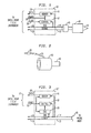
- a probe connector 10 houses a memory 11 and a control circuit 12.
- the ordinary function of the probe with respect to acquiring signal information from a circuit under test is provided by a signal line 13 and a ground line 14. That function is conventional and is not part of the present invention, except that memory 11 and control circuit 12 are connected to the same ground line 14.
- Connector 10 which is suitably adapted for attachment to an intelligent test and measurement (T&M) instrument (not shown), is coupled through a cable 15 to a conventional probe body 16, the tip 17 of which may be used to contact a circuit under test.
- T&M intelligent test and measurement
- Memory 11 comprises a conventional digital memory device, and may be a read-only-memory - (ROM), a programmable read-only-memory - (PROM), a programmable logic array (PLA) or the like.
- ROM read-only-memory -
- PROM programmable read-only-memory -
- PDA programmable logic array
- Memory 11 is programmed at the time of manufacture of the probe assembly with a predetermined set of digital data, -selected for purposes to be noted below.
- Control circuit 12 serves to control the transmission, through data line 18, of the digital data so encoded into memory 11 to an attached T&M instrument.
- Both memory 11 and control circuit 12 require electrical power, which is provided by a power line 19 as shown in Fig. 1.
- a clock line 20 provides a clocking signal from the T&M instrument for the timing of various operations according to the invention, as will be described.
- memory 11 may be a 1 x 2 k bit ROM, and control circuit 12 a simple k-bit counter. The data encoded into memory 11 may then be transmitted sequentially to the T&M instrument upon imposition of a clocking signal on clock line 20 from the T&M instrument.
- the function of the data line 18, power line 19 and clock line 20 is distinct from that of the signal line 13 (and ground line 14), and may use a separate mechanical connection to the T&M instrument.
- a separate mechanical connection to the T&M instrument.
- all of such former lines, and other lines to be discussed hereinafter may be incorporated into a separate multi-lead cable 21 terminated by a conventional stereo plug 22, the latter being adapted for connection to the T&M instrument.
- Such a means of connection also provides a conspicuous indication that a particular probe assembly in fact embodies the present invention.
- the data to be encoded into memory 11 may include such items as the probe type nomenclature and perhaps an individual serial number. Other data that would typically appear in a type specificaton sheet may also be included. The quantity of data that may be encoded into the probe assembly in this manner will of course be limited by the size of memory 11.
- the present invention does not itself seek to encompass the several functions that a T&M instrument may have which will earn it the "intelligent” appellation. These functions are well known in the art, either with respect to a T&M instrument (e.g., an oscilloscope) as such or to computers and microprocessor-controlled devices in general. As noted, standard code formats have then been developed to make the utilization of such art more effective. Even so, it is useful to discuss the present invention in the context of such "intelligent" functions, in order that the advantages of the present invention may be seen, and its several embodiments to be discussed below may be better understood.
- an instrument it is well known for an instrument to be capable of receiving and storing digital data. That is a requirement, of course, in order for the instrument to take advantage of the present invention, ' which seeks to transmit such data thereto through data line 18.
- an instrument in order to utilize the embodiment of the present invention as described with reference to Fig. 1, such an instrument must also be capable of generating and transmitting an appropriate clock signal on clock line 20.
- An alternative embodiment of the invention eliminates the need for transmitting such a clock signal from the T&M instrument, and thus eliminates one of the lines (i.e., clock line 20) that must be carried in cable 21.
- a probe connector 10' additionally houses an oscillator 23, which may be of conventional design and is also connected to ground line 14 and to power line 19.
- the output of oscillator 23 is connected to control circuit 12 and transmits timing pulses thereto in order to bring about a transmission of digital data from memory 11 to the data line 18 as previously discussed.
- Oscillator 23 may be designed to operate at a frequency near that of the clocking signal within the T&M instrument, but not synchronized therewith. In order to provide such synchronization, it is necessary for the T&M instrument to be able to determine the frequency of oscillator 23. The T&M instrument must then be capable of sampling the data appearing on data line 18 at a much faster rate than the latter appears, say, at four times the frequency of oscillator 23. Use of an alternative coding for the data words will then permit them to be counted as they appear at the T&M instrument.
- memory 11 may also be programmed after manufacture, i.e., when being employed in conjunction with a T&M instrument, then permits the storage within memory 11 of data pertaining to specific measurement conditions, and in a non-volatile manner.
- Fig. 4 an embodiment of the invention in which connector 10 houses an electrically alterable read-only-memory - (EAROM) 11' in place of the memory 11 previously employed.
- EAROM electrically alterable read-only-memory -
- R/W Read/Write
- Fig. 4 may then be further modified to allow connection between the probe assembly and the T&M instrument, other than for signal and ground purposes, to be made with three lines within cable 21 rather than the four lines as shown in Fig. 4.
- a simple Read/Write-Clock (RWC) line 25 is provided, and the respective Read/Write and Clock signals are separated out within connector 10.
- RWC Read/Write-Clock
- An expanded view of a portion of connector 10 is shown in Fig. 5 to contain a capacitor 26 and a comparator 27 which will separate those signals as shown in a conventional manner.
- a T&M instrument In order to make use of the embodiments of the invention shown in Figs. 4 or 5, a T&M instrument must have the capability (1) of transmitting Read/Write signals over R/W line 24 with respect to the embodiment of Fig. 4, or of transmitting a Read/Write-Clock signal over RWC line 25 with respect to the embodiment of Fig. 5, and (2) of transmitting digital data over data line 18 to be stored'fn EAROM 11'.
- data may include information acquired through actual use of the probe that was not available at the time of its manufacture.
- Such information may include such items as specific compensation data, i.e., with which particular T&M instrument it had been compensated, on what date, resulting in what specific probe setting for proper compensation, and the like.
- the T&M instrument must also be capable of accepting such data from the user, as by key entry or otherwise, and then storing such data for subsequent writing into EAROM 11' as previously stated.
- the T&M instrument In order to use the information stored in EAROM 11', the T&M instrument must have the capability of reading such data through data line 18 and then presenting it to the user in some fashion. That presentation may be by a simple screen display, or by generation of error messages, e.g., as when a probe assembly is connected to a specific T&M instrument with which it has not previously been employed.
- the invention is instead concerned with the use of such procedures, in the manner described, as part of the electronic T&M procedure and as an aid thereto.
- a memory such as EAROM 11' within the probe assembly
Abstract
Description
- This invention relates to probe devices for connecting an electronic circuit under test to a measurement instrument, and more specifically to self- diagnosing probes which provide to the measurement instrument information concerning the identification and status of the probe itself.
- The very wide variety of modem electronic equipment creates a similar variety of testing and measurement (T&M) requirements, and a need in each case to establish a proper test setup. That setup includes both the appropriate T&M instrumentation and the signal acquisition probes which will connect to the circuitry under test. In view of the numerous different T&M situations that may be encountered the probes to be employed must also be available in a number of different types and configurations.
- Such probes may be active or passive, current or voltage sensing, or impedance matching. With respect to digital devices, such probes may contain a number of data channels and may vary as to their threshold voltages, bandwidths, or input resistance or capacitance. Similar variations may occur in the output or termination circuitry of such probes. For use with digital analyzers, such probes may include clock inputs to the measurement instrument, or clock or data qualification of the data to be transmitted.
- A signal acquisition probe may also be multipurpose, having several internal configurations with respect to attenuation, channel access or the like that are switch-selectable. Similarly, a probe may incorporate a compensation capacitor for adjusting the probe's response to high frequency signals, or digital compensation circuitry for achieving proper compensation of an analog signal. A probe may also have separate head, cable, and termination units, the proper combination of which are assembled for a particular measurement situation.
- In any of these cases, or in other cases that will be known to persons of ordinary skill in the art, the use of a "wrong" probe or of a probe which is not properly calibrated, compensated, or otherwise appropriately configured, may introduce substantial error into the T&M process. Because of the subtle variations that may exist even among probes or test instruments of a given type, selection of the "correct" probe and configuration may have to be carried out with respect to each individual instrument.
- Simply to set up for a measurement, therefore, may become a complex and time-consuming process. Such complexity may derive not only from the selection process itself, but also from the need to maintain records of the information necessary to make that selection correctly.
- It would thus be useful to have immediate access to the information necessary to carry out a T&M setup, or at least to confirm that a setup has been correctly made. To aid in such setting up, the probes themselves and their various components typically carry labels that identify their type. Similarly, one may usually determine whether probe switches, such as an attenuator switch, are set correctly. However, one can not look at a probe and determine whether it is properly compensated, or is otherwise correctly configured internally. Also, some external indicia is needed to determine whether a particular probe of the required type is one which happens to work best, say, with a particular oscilloscope. It would then be useful as well to have that kind of information provided otherwise, and preferably by the probe itself.
- It has become a standard practice in the electronics art to provide microprocessor control of T&M instruments, many of which have the capability of transmitting and receiving digital data and instructions. A significant number of such instruments also have the ability to provide visual displays of the data so treated, and to generate error messages therefrom. Interface between instruments having such capability is very often through systems of a standard design, such as the IEEE-488 General Purpose Interface Bus (GPIB). A code format such as ANSI X3.42 must also be employed, and a code selected such as ASCII or EBCDIC. In Tektronix instruments, for example, ASCII code having the most significant data first is employed uniformly.
- However, very few prior art electrical or electronic probes convey any information other than electrical signal data from a circuit under test. In particular, little or no information is conveyed as to the probe's identification or status, except such as is apparent from its gross appearance and through the information printed on its label. Limited additional information can be found through use of such probes as the P6053B, P6055, P6062B and P6063 series of passive probes manufactured by Tektronix, Inc., which provide a direct digital readout of their attenuation settings to the oscilloscope to which they are connected. Another means for conveying information other than T&M signals from a probe to a screen is found in systems for trace identification, i.e., an operator may "key" the probe to cause visible indication on the screen of the particular trace corresponding to that probe when operating in a dual-trace mode.
- Absent such electronic indication processes, only the probe or component type, and perhaps some limited information with respect to voltage ratings and the like, can be derived from the probe itself and its labelling. Other information of interest must be derived, for example, from an associated specification sheet or manual. Even then, little may be learned from a type specification table concerning the detailed characteristics of a particular probe of the type, what individual variations in such characteristics may result from the use of different cables or terminations, and certainly nothing with respect, say, to the compensation status of a probe at a particular time, or what compensation setting the probe ought to have in particular cases.
- It would then be useful as well, once a probe has been optimally configured for a given measurement situation, in terms both of the probe combination itself and of and probe adjustments that can be made, to be able to recapture that information after the probe has been laid aside. Without such recapture, it may be necessary, for example, to reconnect the probe to an appropriate signal source and re-compensate, and perhaps to re-confirm by other means that the most suitable combination of head, cable, and termination is being employed.
- Again, it would be desirable to have the probe itself provide the necessary information as to the configuration needed for particular purposes, with which specific T&M equipment it should be employed, its proper compensation or attenuation settings, optional cable lengths, and the like. Similarly, when a probe has been connected for a particular measurement situation, information should be provided which will establish whether that configuration is appropriate or not. It is to such objectives that the present invention is directed, together with such other objectives and advantages as will, from the nature of this invention, become apparent to those persons having ordinary skill in the art.
- A probe assembly in accordance with the invention includes a memory into which may be recorded such status information as the probe type, serial number, and type specification data. Means for transmitting such information to a test and measurement (T&M) instrument for display or for the generation of error messages are provided, along with the channels for transmitting T&M data. Transmission of such status data is controlled by a clock either within the T&M instrument or the probe assembly itself.
- In another embodiment of the invention, data that are derived from actual use of the probe assembly may be entered into the T&M instrument and then stored in the probe assembly for future reference.
-
- FIG. 1 shows in block diagram form a first embodiment of the invention.
- FIG. 2 illustrates pictorially a means for making mechanical connection of a device embodying the invention to a test and measurement instrument.
- FIG. 3 shows in block diagram a second embodiment of the invention in the form of a device that incorporates an oscillator for generating timing signals.
- FIG. 4 shows in block diagram a third embodiment of the invention in the form of a device configured for transmitting data to and from the device.
- FIG. 5 shows in a partial circuit diagram a form of the device of Fig. 4 in which READ/WRITE and
clock 20 signals may be separated within the device. - A first, relatively simple embodiment of the present invention is illustrated in Fig. 1. A
probe connector 10 houses amemory 11 and acontrol circuit 12. The ordinary function of the probe with respect to acquiring signal information from a circuit under test is provided by asignal line 13 and aground line 14. That function is conventional and is not part of the present invention, except thatmemory 11 andcontrol circuit 12 are connected to thesame ground line 14.Connector 10, which is suitably adapted for attachment to an intelligent test and measurement (T&M) instrument (not shown), is coupled through acable 15 to aconventional probe body 16, thetip 17 of which may be used to contact a circuit under test. -
Memory 11 comprises a conventional digital memory device, and may be a read-only-memory - (ROM), a programmable read-only-memory - (PROM), a programmable logic array (PLA) or the like. In this simple embodiment of the invention,memory 11 is programmed at the time of manufacture of the probe assembly with a predetermined set of digital data, -selected for purposes to be noted below.Control circuit 12 serves to control the transmission, throughdata line 18, of the digital data so encoded intomemory 11 to an attached T&M instrument. - Both
memory 11 andcontrol circuit 12 require electrical power, which is provided by apower line 19 as shown in Fig. 1. In addition, aclock line 20 provides a clocking signal from the T&M instrument for the timing of various operations according to the invention, as will be described. For example,memory 11 may be a 1 x 2k bit ROM, and control circuit 12 a simple k-bit counter. The data encoded intomemory 11 may then be transmitted sequentially to the T&M instrument upon imposition of a clocking signal onclock line 20 from the T&M instrument. - As noted, the function of the
data line 18,power line 19 andclock line 20 is distinct from that of the signal line 13 (and ground line 14), and may use a separate mechanical connection to the T&M instrument. For example, as shown in Fig. 2, all of such former lines, and other lines to be discussed hereinafter, may be incorporated into aseparate multi-lead cable 21 terminated by aconventional stereo plug 22, the latter being adapted for connection to the T&M instrument. Such a means of connection also provides a conspicuous indication that a particular probe assembly in fact embodies the present invention. - In using serial transmission of data through
data line 18, there is no need for start/stop addressing. Through proper encoding, the beginning and end of the data sequence may also be recognized by the T&M instrument. In operation, a convenient code such as ASCII must also be employed. An 8-bit ASCII code in therange 20 to 5 F with the most significant bit being 0 is then employed. The start of the data is indicated by a three-word sequence of 8 zeros, followed by 8 ones, and then 8 zeroes. Conversely, the end of the data is indicated by a sequence of 8 ones, followed by 8 zeroes, and then 8 ones. The use of such start/stop encoding then leaves 122 additional ASCII words available in a 1024-bit memory, or 250 such words in a 2048-bit memory. Unused words may be encoded as a "space" (ASCII 20). - The data to be encoded into
memory 11 may include such items as the probe type nomenclature and perhaps an individual serial number. Other data that would typically appear in a type specificaton sheet may also be included. The quantity of data that may be encoded into the probe assembly in this manner will of course be limited by the size ofmemory 11. - The present invention does not itself seek to encompass the several functions that a T&M instrument may have which will earn it the "intelligent" appellation. These functions are well known in the art, either with respect to a T&M instrument (e.g., an oscilloscope) as such or to computers and microprocessor-controlled devices in general. As noted, standard code formats have then been developed to make the utilization of such art more effective. Even so, it is useful to discuss the present invention in the context of such "intelligent" functions, in order that the advantages of the present invention may be seen, and its several embodiments to be discussed below may be better understood.
- Thus, it is well known for an instrument to be capable of receiving and storing digital data. That is a requirement, of course, in order for the instrument to take advantage of the present invention, ' which seeks to transmit such data thereto through
data line 18. In addition, in order to utilize the embodiment of the present invention as described with reference to Fig. 1, such an instrument must also be capable of generating and transmitting an appropriate clock signal onclock line 20. An alternative embodiment of the invention eliminates the need for transmitting such a clock signal from the T&M instrument, and thus eliminates one of the lines (i.e., clock line 20) that must be carried incable 21. - Specifically, in Fig. 3 there is shown an embodiment of the invention in which a probe connector 10' additionally houses an
oscillator 23, which may be of conventional design and is also connected to groundline 14 and topower line 19. The output ofoscillator 23 is connected to controlcircuit 12 and transmits timing pulses thereto in order to bring about a transmission of digital data frommemory 11 to thedata line 18 as previously discussed. -
Oscillator 23 may be designed to operate at a frequency near that of the clocking signal within the T&M instrument, but not synchronized therewith. In order to provide such synchronization, it is necessary for the T&M instrument to be able to determine the frequency ofoscillator 23. The T&M instrument must then be capable of sampling the data appearing ondata line 18 at a much faster rate than the latter appears, say, at four times the frequency ofoscillator 23. Use of an alternative coding for the data words will then permit them to be counted as they appear at the T&M instrument. - Such an alternative coding is shown below in Table I:

- By substituting the sequences AO -AF and BO - BF for 20 -2F and 30 -3F, respectively, it is then established that, if the Most Significant Bit (MSB) of each word is sent first, the appearance of a word in every case will be signified by the appearance either of a one bracketed by two zeroes, or by a zero bracketed by two ones. A counter within the T&M instrument encoded to respond to those bit patterns will then count each such word as it appears and may then force the writing of such data into memory within the instrument into synchrony with
oscillator 23. - The embodiments of the invention as previously described represent cases in which permanently encoded data are employed. An alternative embodiment in which
memory 11 may also be programmed after manufacture, i.e., when being employed in conjunction with a T&M instrument, then permits the storage withinmemory 11 of data pertaining to specific measurement conditions, and in a non-volatile manner. - Specifically, there is shown in Fig. 4 an embodiment of the invention in which
connector 10 houses an electrically alterable read-only-memory - (EAROM) 11' in place of thememory 11 previously employed. In addition, a Read/Write (R/W)line 24 connects throughcable 21 from EAROM 11' to the T&M instrument. The other elements included in this embodiment of the invention are the same as those shown in Fig. 1. - The embodiment of the invention shown in Fig. 4 may then be further modified to allow connection between the probe assembly and the T&M instrument, other than for signal and ground purposes, to be made with three lines within
cable 21 rather than the four lines as shown in Fig. 4. As is then shown in Fig. 5, a simple Read/Write-Clock (RWC)line 25 is provided, and the respective Read/Write and Clock signals are separated out withinconnector 10. An expanded view of a portion ofconnector 10 is shown in Fig. 5 to contain acapacitor 26 and acomparator 27 which will separate those signals as shown in a conventional manner. - In order to make use of the embodiments of the invention shown in Figs. 4 or 5, a T&M instrument must have the capability (1) of transmitting Read/Write signals over R/
W line 24 with respect to the embodiment of Fig. 4, or of transmitting a Read/Write-Clock signal overRWC line 25 with respect to the embodiment of Fig. 5, and (2) of transmitting digital data overdata line 18 to be stored'fn EAROM 11'. For purposes of assisting in the T&M setup process, such data may include information acquired through actual use of the probe that was not available at the time of its manufacture. Such information may include such items as specific compensation data, i.e., with which particular T&M instrument it had been compensated, on what date, resulting in what specific probe setting for proper compensation, and the like. The T&M instrument must also be capable of accepting such data from the user, as by key entry or otherwise, and then storing such data for subsequent writing into EAROM 11' as previously stated. - In order to use the information stored in EAROM 11', the T&M instrument must have the capability of reading such data through
data line 18 and then presenting it to the user in some fashion. That presentation may be by a simple screen display, or by generation of error messages, e.g., as when a probe assembly is connected to a specific T&M instrument with which it has not previously been employed. These and the procedures previously described that relate only to the T&M instrument itself do not constitute a part of the present invention. - The invention is instead concerned with the use of such procedures, in the manner described, as part of the electronic T&M procedure and as an aid thereto. For that purpose, while the foregoing description has been given in terms of particular examples of the kinds of information that can be stored into and retrieved from a memory such as EAROM 11' within the probe assembly, and also in terms of particular embodiments of the invention and variations thereof, it should be understood that no limitation in the scope of the invention is thereby intended, since a very many such variations upon the present invention will be apparent to those of ordinary skill in the art. Consequently, the scope of the present invention should be interpreted only from the claims appended hereto, and from the equivalents thereof.
Claims (8)
Applications Claiming Priority (2)
| Application Number | Priority Date | Filing Date | Title |
|---|---|---|---|
| US06/720,762 US4672306A (en) | 1985-04-08 | 1985-04-08 | Electronic probe having automatic readout of identification and status |
| US720762 | 1985-04-08 |
Publications (2)
| Publication Number | Publication Date |
|---|---|
| EP0201181A1 true EP0201181A1 (en) | 1986-12-17 |
| EP0201181B1 EP0201181B1 (en) | 1990-11-14 |
Family
ID=24895188
Family Applications (1)
| Application Number | Title | Priority Date | Filing Date |
|---|---|---|---|
| EP86302244A Expired - Lifetime EP0201181B1 (en) | 1985-04-08 | 1986-03-26 | Probe assembly for use with electronic instrument |
Country Status (5)
| Country | Link |
|---|---|
| US (1) | US4672306A (en) |
| EP (1) | EP0201181B1 (en) |
| JP (1) | JPH083511B2 (en) |
| CA (1) | CA1241060A (en) |
| DE (1) | DE3675575D1 (en) |
Cited By (3)
| Publication number | Priority date | Publication date | Assignee | Title |
|---|---|---|---|---|
| EP0241142A1 (en) * | 1986-04-07 | 1987-10-14 | Tektronix, Inc. | Probe body for an electrical measurement system |
| EP0984287A1 (en) * | 1998-08-31 | 2000-03-08 | Hewlett-Packard Company | Oscilloscope probe having stored probe identification |
| KR101127018B1 (en) | 2004-02-25 | 2012-04-12 | 텍트로닉스 인코포레이티드 | Calibration method and apparatus |
Families Citing this family (41)
| Publication number | Priority date | Publication date | Assignee | Title |
|---|---|---|---|---|
| US4949274A (en) * | 1987-05-22 | 1990-08-14 | Omega Engineering, Inc. | Test meters |
| AU1809888A (en) * | 1987-05-22 | 1988-12-21 | Omega Engineering, Inc. | Test meters |
| US5050106A (en) * | 1987-10-07 | 1991-09-17 | Omron Tateisi Electronics Co. | Article recognizing system |
| US4840066A (en) * | 1988-06-27 | 1989-06-20 | Ndt Instruments, Inc. | Ultrasonic thickness gauge having automatic transducer recognition and parameter optimization and method thereof |
| US5162725A (en) * | 1989-08-21 | 1992-11-10 | Alnor Instrument Company | Modular metering instrument including multiple sensing probes |
| US6347240B1 (en) | 1990-10-19 | 2002-02-12 | St. Louis University | System and method for use in displaying images of a body part |
| DE69132412T2 (en) | 1990-10-19 | 2001-03-01 | Univ St Louis | LOCALIZATION SYSTEM FOR A SURGICAL PROBE FOR USE ON THE HEAD |
| US5603318A (en) | 1992-04-21 | 1997-02-18 | University Of Utah Research Foundation | Apparatus and method for photogrammetric surgical localization |
| US5248933A (en) * | 1992-06-15 | 1993-09-28 | Thornton Associates, Inc. | Calibration |
| US5359283A (en) * | 1993-03-29 | 1994-10-25 | Brooklyn Computer Systems Inc. | Hand held wand for transferring data from one device to another |
| CA2161430C (en) | 1993-04-26 | 2001-07-03 | Richard D. Bucholz | System and method for indicating the position of a surgical probe |
| US5546082A (en) * | 1994-04-22 | 1996-08-13 | Rosemount Analytical Inc. | Measurement probe with improved analog-to-digital conversion |
| CA2201877C (en) | 1994-10-07 | 2004-06-08 | Richard D. Bucholz | Surgical navigation systems including reference and localization frames |
| US6978166B2 (en) * | 1994-10-07 | 2005-12-20 | Saint Louis University | System for use in displaying images of a body part |
| US5617857A (en) * | 1995-06-06 | 1997-04-08 | Image Guided Technologies, Inc. | Imaging system having interactive medical instruments and methods |
| US5790432A (en) * | 1995-08-21 | 1998-08-04 | Solar Light Company, Inc. | Universal measuring instrument with signal processing algorithm encapsulated into interchangeable intelligent detectors |
| US5566680A (en) * | 1995-09-22 | 1996-10-22 | Graphic Controls Corporation | Transducer-tipped intrauterine pressure catheter system |
| US5691635A (en) * | 1996-01-29 | 1997-11-25 | Fluke Corporation | Probe identification system for a measurement instrument |
| US6167145A (en) * | 1996-03-29 | 2000-12-26 | Surgical Navigation Technologies, Inc. | Bone navigation system |
| US6305963B1 (en) * | 1996-08-16 | 2001-10-23 | Agilent Technologies, Inc. | Push-lock BNC connector |
| US5939875A (en) * | 1997-03-17 | 1999-08-17 | Hewlett-Packard Company | Universal probe interface |
| US6021343A (en) | 1997-11-20 | 2000-02-01 | Surgical Navigation Technologies | Image guided awl/tap/screwdriver |
| US6232764B1 (en) | 1998-06-12 | 2001-05-15 | Tektronix, Inc. | Accessory with internal adjustments controlled by host |
| US6385550B1 (en) * | 1998-06-15 | 2002-05-07 | Tektronix, Inc. | Apparatus and method for providing forward and backward compatibility between a host instrument and an accessory |
| WO2000060558A1 (en) * | 1999-04-06 | 2000-10-12 | Thornton Associates, Inc. | Multiplexing sensor signals |
| US6517359B1 (en) | 1999-05-21 | 2003-02-11 | Agilent Technologies, Inc. | System and method for mating electrical connections |
| US6629048B1 (en) * | 2000-11-20 | 2003-09-30 | Tektronix, Inc. | Measurement test instrument and associated voltage management system for accessory device |
| US6725170B1 (en) * | 2000-11-22 | 2004-04-20 | Tektronix, Inc. | Smart probe apparatus and method for automatic self-adjustment of an oscilloscope's bandwidth |
| US6524123B2 (en) | 2001-01-19 | 2003-02-25 | Agilent Technologies, Inc. | Self-aligning, quick-release connector |
| US6956362B1 (en) | 2001-12-14 | 2005-10-18 | Lecroy Corporation | Modular active test probe and removable tip module therefor |
| US6829547B2 (en) * | 2002-04-29 | 2004-12-07 | Tektronix, Inc. | Measurement test instrument and associated voltage management system for accessory device |
| US7003317B2 (en) * | 2003-01-24 | 2006-02-21 | Belcher Willie S | Motorcycle helmet communication cable |
| US7308519B2 (en) * | 2003-01-31 | 2007-12-11 | Tektronix, Inc. | Communications bus management circuit |
| US7109728B2 (en) * | 2003-02-25 | 2006-09-19 | Agilent Technologies, Inc. | Probe based information storage for probes used for opens detection in in-circuit testing |
| DE10357856B4 (en) * | 2003-12-11 | 2008-01-03 | Sartorius Ag | measuring device |
| US7634374B2 (en) * | 2004-04-26 | 2009-12-15 | Orthosoft Inc. | Method for permanent calibration based on actual measurement |
| US7532492B2 (en) * | 2005-12-20 | 2009-05-12 | Tektronix, Inc. | Host controlled voltage input system for an accessory device |
| DE102010063970A1 (en) * | 2010-12-22 | 2012-06-28 | Endress + Hauser Conducta Gesellschaft für Mess- und Regeltechnik mbH + Co. KG | Retractable housing |
| US9188606B2 (en) | 2013-04-29 | 2015-11-17 | Keysight Technologies, Inc. | Oscilloscope current probe with interchangeable range and sensitivity setting modules |
| US11287445B2 (en) | 2018-10-29 | 2022-03-29 | Keysight Technologies, Inc. | Oscilloscope probe identification |
| CN115469125A (en) * | 2022-10-13 | 2022-12-13 | 普源精电科技股份有限公司 | Oscilloscope probe, probe detection method, device, oscilloscope, system and medium |
Citations (3)
| Publication number | Priority date | Publication date | Assignee | Title |
|---|---|---|---|---|
| DE2631483A1 (en) * | 1976-07-13 | 1978-01-19 | Siemens Ag | Automatic test equipment for plug:in modules - has encoded test module determining its own test routine and permitting program to be varied accordingly |
| EP0067510A2 (en) * | 1981-06-05 | 1982-12-22 | John Fluke Mfg. Co., Inc. | A test system for functionally testing a microprocessor-based assembly, and apparatus for testing logic circuitry |
| EP0115566A2 (en) * | 1982-12-09 | 1984-08-15 | International Business Machines Corporation | Method for testing the operation of an I/O controller in a data processing system |
Family Cites Families (6)
| Publication number | Priority date | Publication date | Assignee | Title |
|---|---|---|---|---|
| JPS5695738A (en) * | 1979-12-26 | 1981-08-03 | Nippon Denso Co Ltd | Method and apparatus for indicating and disposing of abnormal condition |
| US4401949A (en) * | 1981-02-02 | 1983-08-30 | Fmc Corporation | External device identification system |
| US4541100A (en) * | 1981-05-15 | 1985-09-10 | Tektronix, Inc. | Apparatus including a programmable set-up and hold feature |
| US4575803A (en) * | 1981-12-30 | 1986-03-11 | Semco Instruments, Inc. | Engine monitor and recorder |
| US4493044A (en) * | 1982-03-08 | 1985-01-08 | Tektronix | Apparatus and a method of establishing the correct display order of probe channels for a logic analyzer |
| GB2129259B (en) * | 1982-09-14 | 1987-04-08 | Analogic Corp | Modular computing oscilloscope |
-
1985
- 1985-04-08 US US06/720,762 patent/US4672306A/en not_active Expired - Lifetime
-
1986
- 1986-03-18 CA CA000504373A patent/CA1241060A/en not_active Expired
- 1986-03-26 DE DE8686302244T patent/DE3675575D1/en not_active Expired - Lifetime
- 1986-03-26 EP EP86302244A patent/EP0201181B1/en not_active Expired - Lifetime
- 1986-04-07 JP JP61079886A patent/JPH083511B2/en not_active Expired - Lifetime
Patent Citations (3)
| Publication number | Priority date | Publication date | Assignee | Title |
|---|---|---|---|---|
| DE2631483A1 (en) * | 1976-07-13 | 1978-01-19 | Siemens Ag | Automatic test equipment for plug:in modules - has encoded test module determining its own test routine and permitting program to be varied accordingly |
| EP0067510A2 (en) * | 1981-06-05 | 1982-12-22 | John Fluke Mfg. Co., Inc. | A test system for functionally testing a microprocessor-based assembly, and apparatus for testing logic circuitry |
| EP0115566A2 (en) * | 1982-12-09 | 1984-08-15 | International Business Machines Corporation | Method for testing the operation of an I/O controller in a data processing system |
Non-Patent Citations (2)
| Title |
|---|
| PATENT ABSTRACTS OF JAPAN, vol. 7, no. 72 (E-166)[1217], 25th March 1983; & JP-A-58 003 256 (FUJITSU) 10-01-1983 * |
| WESCON TECHNICAL PAPER, vol. 26, September 1982, pages 1-4; K.R. HALLMEN "Synchronous address space testing" * |
Cited By (4)
| Publication number | Priority date | Publication date | Assignee | Title |
|---|---|---|---|---|
| EP0241142A1 (en) * | 1986-04-07 | 1987-10-14 | Tektronix, Inc. | Probe body for an electrical measurement system |
| EP0984287A1 (en) * | 1998-08-31 | 2000-03-08 | Hewlett-Packard Company | Oscilloscope probe having stored probe identification |
| US6351112B1 (en) | 1998-08-31 | 2002-02-26 | Agilent Technologies, Inc. | Calibrating combinations of probes and channels in an oscilloscope |
| KR101127018B1 (en) | 2004-02-25 | 2012-04-12 | 텍트로닉스 인코포레이티드 | Calibration method and apparatus |
Also Published As
| Publication number | Publication date |
|---|---|
| JPS61235763A (en) | 1986-10-21 |
| CA1241060A (en) | 1988-08-23 |
| DE3675575D1 (en) | 1990-12-20 |
| JPH083511B2 (en) | 1996-01-17 |
| US4672306A (en) | 1987-06-09 |
| EP0201181B1 (en) | 1990-11-14 |
Similar Documents
| Publication | Publication Date | Title |
|---|---|---|
| EP0201181B1 (en) | Probe assembly for use with electronic instrument | |
| US6351112B1 (en) | Calibrating combinations of probes and channels in an oscilloscope | |
| EP0056895B1 (en) | Automatic test system | |
| US7532492B2 (en) | Host controlled voltage input system for an accessory device | |
| US5027074A (en) | Cable tester | |
| US5691635A (en) | Probe identification system for a measurement instrument | |
| EP0008954A1 (en) | Computerized test system for testing an electrical harness and a method of testing an electrical harness | |
| US4399400A (en) | Apparatus for testing multiconductor cables and having transition circuit means for extending its capability | |
| US5939875A (en) | Universal probe interface | |
| US4317199A (en) | Diagnostic extender test apparatus | |
| AU616895B2 (en) | Programmable tester with bubble memory | |
| JPS6366470A (en) | Probe device | |
| US20050083067A1 (en) | Coded multi-frequency transmitter and receiver for testing multi-conductor cables | |
| US5248933A (en) | Calibration | |
| EP0157028A1 (en) | Programmable tester | |
| US4701696A (en) | Retargetable buffer probe | |
| US6385550B1 (en) | Apparatus and method for providing forward and backward compatibility between a host instrument and an accessory | |
| EP0844562A2 (en) | Method and apparatus for producing self-diagnostic information from a circuit board | |
| US6052807A (en) | Multiple probe test equipment with channel identification | |
| US4737955A (en) | Switch closure test method and apparatus | |
| EP0004153A1 (en) | Method and apparatus for comparing logic functions | |
| KR960006964Y1 (en) | Interface for measurement of electric current in human-body |
Legal Events
| Date | Code | Title | Description |
|---|---|---|---|
| PUAI | Public reference made under article 153(3) epc to a published international application that has entered the european phase |
Free format text: ORIGINAL CODE: 0009012 |
|
| AK | Designated contracting states |
Kind code of ref document: A1 Designated state(s): DE FR GB NL |
|
| PUAB | Information related to the publication of an a document modified or deleted |
Free format text: ORIGINAL CODE: 0009199EPPU |
|
| PUAF | Information related to the publication of a search report (a3 document) modified or deleted |
Free format text: ORIGINAL CODE: 0009199SEPU |
|
| R17D | Deferred search report published (corrected) |
Effective date: 19861217 |
|
| RA1 | Application published (corrected) |
Date of ref document: 19861217 Kind code of ref document: A1 |
|
| 17P | Request for examination filed |
Effective date: 19870105 |
|
| 17Q | First examination report despatched |
Effective date: 19890203 |
|
| RAP1 | Party data changed (applicant data changed or rights of an application transferred) |
Owner name: TEKTRONIX, INC. |
|
| GRAA | (expected) grant |
Free format text: ORIGINAL CODE: 0009210 |
|
| AK | Designated contracting states |
Kind code of ref document: B1 Designated state(s): DE FR GB NL |
|
| REF | Corresponds to: |
Ref document number: 3675575 Country of ref document: DE Date of ref document: 19901220 |
|
| ET | Fr: translation filed | ||
| PLBE | No opposition filed within time limit |
Free format text: ORIGINAL CODE: 0009261 |
|
| STAA | Information on the status of an ep patent application or granted ep patent |
Free format text: STATUS: NO OPPOSITION FILED WITHIN TIME LIMIT |
|
| 26N | No opposition filed | ||
| REG | Reference to a national code |
Ref country code: GB Ref legal event code: IF02 |
|
| PGFP | Annual fee paid to national office [announced via postgrant information from national office to epo] |
Ref country code: NL Payment date: 20050211 Year of fee payment: 20 Ref country code: FR Payment date: 20050211 Year of fee payment: 20 |
|
| PGFP | Annual fee paid to national office [announced via postgrant information from national office to epo] |
Ref country code: GB Payment date: 20050214 Year of fee payment: 20 |
|
| PGFP | Annual fee paid to national office [announced via postgrant information from national office to epo] |
Ref country code: DE Payment date: 20050216 Year of fee payment: 20 |
|
| PG25 | Lapsed in a contracting state [announced via postgrant information from national office to epo] |
Ref country code: GB Free format text: LAPSE BECAUSE OF EXPIRATION OF PROTECTION Effective date: 20060325 |
|
| PG25 | Lapsed in a contracting state [announced via postgrant information from national office to epo] |
Ref country code: NL Free format text: LAPSE BECAUSE OF EXPIRATION OF PROTECTION Effective date: 20060326 |
|
| REG | Reference to a national code |
Ref country code: GB Ref legal event code: PE20 |
|
| NLV7 | Nl: ceased due to reaching the maximum lifetime of a patent |
Effective date: 20060326 |