EP0181174A2 - A matrix-addressed display device - Google Patents
A matrix-addressed display device Download PDFInfo
- Publication number
- EP0181174A2 EP0181174A2 EP85307963A EP85307963A EP0181174A2 EP 0181174 A2 EP0181174 A2 EP 0181174A2 EP 85307963 A EP85307963 A EP 85307963A EP 85307963 A EP85307963 A EP 85307963A EP 0181174 A2 EP0181174 A2 EP 0181174A2
- Authority
- EP
- European Patent Office
- Prior art keywords
- signal
- sampling frequency
- matrix
- horizontal
- oscillation
- Prior art date
- Legal status (The legal status is an assumption and is not a legal conclusion. Google has not performed a legal analysis and makes no representation as to the accuracy of the status listed.)
- Granted
Links
Images

Classifications
-
- G—PHYSICS
- G09—EDUCATION; CRYPTOGRAPHY; DISPLAY; ADVERTISING; SEALS
- G09F—DISPLAYING; ADVERTISING; SIGNS; LABELS OR NAME-PLATES; SEALS
- G09F9/00—Indicating arrangements for variable information in which the information is built-up on a support by selection or combination of individual elements
-
- H—ELECTRICITY
- H04—ELECTRIC COMMUNICATION TECHNIQUE
- H04N—PICTORIAL COMMUNICATION, e.g. TELEVISION
- H04N3/00—Scanning details of television systems; Combination thereof with generation of supply voltages
- H04N3/10—Scanning details of television systems; Combination thereof with generation of supply voltages by means not exclusively optical-mechanical
- H04N3/12—Scanning details of television systems; Combination thereof with generation of supply voltages by means not exclusively optical-mechanical by switched stationary formation of lamps, photocells or light relays
- H04N3/127—Scanning details of television systems; Combination thereof with generation of supply voltages by means not exclusively optical-mechanical by switched stationary formation of lamps, photocells or light relays using liquid crystals
Definitions
- This invention relates to a matrix-addressed display device that displays for example a TV picture, more particularly to the construction of a sampling frequency generator in serial-parallel conversion by sampling the input picture signal.
- Serial-parallel conversion means that serial data, i.e. data that is time-serially transmitted on a single transmission line, is converted to parallel data that is simultaneously transmitted on a plurality of transmission lines. Such serial-parallel conversion is utilized in a matrix-addressed display device that is driven by one-line- at-a-time addressing.
- a typical matrix-addressed liquid ctystal display device has a rectangular display panel consisting of thin film transistors (TFT) arranged in a matrix constituted by the points of intersection of respective signal lines X1, ..., Xm and address lines Y1, ..., Yn, which are provided in the horizontal direction (X axis direction or main addressing direction) and vertical direction (Y axis direction or ancillary addressing direction).
- TFT thin film transistors
- a picture signal source, frame inverting amplifier, synchronizing signal separator, control circuit, Y driver and X driver are arranged around the periphery of the display panel.
- the X driver is provided with a sampling pulse generator and sample and hold circuit.
- the picture elements within the liquid crystal display panel are constituted by a TFT, a signal storage capacitor, a liquid crystal cell and a counter electrode common to all the picture elements.
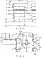
- Fig. 6 is a waveform "diagram given in explanation of the operation of such a display device.
- a and b are respectively the vertical synchronizing signal and horizontal synchronizing signal obtained at the output of the synchronizing signal separator.
- c is the vertical scanning start signal. This is generated under the control of the abovementioned synchronizing signals.
- Horizontal synchronizing signal b and vertical scanning start signal c are fed to the Y driver to address, one line at a time, the address lines Y1, ..., Yn of the liquid crystal display panel.
- d is the picture signal. This is supplied from the picture signal source through the frame inverting amplifier to the sample and hold circuit. The drawing shows the period of a single horizontal scan.
- el and f are respectively the sampling frequency signal and horizontal scanning start signal. These signals are generated under the control of the horizontal synchronizing signal b. It should be noted that, in the Figure, the length of the time axis of the other signals shown below signal d is the same as in the case of signal d itself.
- sampling frequency signal el and the horizontal scanning signal f are supplied to the sampling pulse generator, which is constituted by a shift register, and generates sampling pulses S1, ..., Sm.
- sampling pulses S1, ..., Sm are supplied to the sample and hold circuit, which converts the picture signal d into a parallel picture signal by a sequential sample-and-hold operation performed with the period of the horizontal scanning.
- the parallel picture signal is simultaneously delivered, under the control of output enable pulse g from the control circuit, from the sample and hold circuit to the signal lines X1, ..., Xm of the liquid crystal panel.
- the picture is displayed by excitation of the liquid crystal cells by the picture signal voltage, which is held for the frame scanning period.
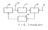
- Fig. 7 shows the construction of a frequency synthesizer in which a PLL (Phase-Locked Loop) is utilized as this sampling frequency generator.
- this sampling frequency generator is composed of a voltage controlled oscillator 10, a counter 11, a phase comparator 12, a low pass filter 13, a reference frequency input terminal 14 and an scillating frequency output terminal 15.
- a desired value for example K
- the sampling frequency generator is constructed of a PLL, fine picture dispaly is difficult to obtain, due to disturbances of the sampling timing resulting from freguency or phase instability of the oscillating output pulse. Furthermore, power is consumed unnecessarily by the fact that the oscillating pulse from the sampling frequency pulse generator is output continuously, even in periods wherein a sampling pulse is not required, such as the period where the output enable pulse g of Fig. 6 is high-level.
- This invention provides a matrix-adderssed display device capable of displaying clear pictures with low power consumption.
- this invention consists in a matrix-addressed display device comprising:
- the sampling frequency generator includes a gated oscillator and a horizontal counter, the gated oscillator being so constructed that it starts oscillation with a timing that is linked to a horizontal synchronizing signal that is either contained in the input picture signal or separately input, the output pulse produced by this oscillation being counted by the horizontal counter so that oscillation is stopped at the point of time at which a number of pulses have been outputted that is related to the number of pixels in the horizontal direction.
- the sampling frequency generator includes a vertical counter and the gated oscillator is of a construction such that it starts oscillating with a timing that is related to the vertical synchronizing signal and the horizontal saychronizing signal, these being either separately input or contained in the input picture signal, and the horizontal synchronizing signal is counted, from this time-point, by the vertical counter until a count value is reached that is related to the number of pixels in the vertical direction, and stopping and starting of oscillation are repeated, with the timing of starting of oscillation being related to the horizontal synchronizing signal.
- Fig. 1 shows s matrix-addressed display device constituting an embodiment of this invention.
- the basic construction of this matrix-addressed display device involves peoducing a display such as a television picture using a thin film transistor TFT array type liquid crystal display panel.
- signal lines X1, ..., Xm and address lines Y1, ..., Yn are arranged in an intersecting manner within the liquid crystal display panel 1, while a picture signal source 2, a frame inverting amplifier 3, a synchronizing signal separator 4, a control circuit 5, a Y driver 6, and a X driver 7 are provided around the periphery of the panel.
- X driver 7 consists of a sampling pulse generator 7 and a sample and hold circuit 7 2 .
- Pixels 8 in the liquid crystal display panel 1 are composed of respective TFT 8 1 , signal storage capacitor 8 , liquid crystal cell 8 3 , and counter electrode 8 4 .
- the output signal from picture signal source 2 is applied to frame inverting amplifier 3 and synchronizing signal separator 4.
- the subsequent waveforms of each signal coincide with the corresponding symbols a to g of Fig. 6.
- Synchronizing signal separator 4 separates vertical synchronizing signal a and horizontal synchronizing signal b from the aforementioned signal and supplies them to control circuet 5.
- Frame inverting amplifier 3 generates picture signal d, inverted in polarity with every frame, in synchronism with the signal from the control circuit, and supplies it to sample and hold circuit 1 2 .
- Control circuit 5 receives vertical synchronizing signal a and horizontal synchronizing signal b and supplies horizontal synchronizing signal b and vertical scanning start signal c, which is synthesized from the synchronizing signals a and b, to Y driver 6. Furthermore, control circuit 5 generates sampling frequency signal e2 and horizontal scanning start signal f based on horizontal synchronizing signal b, and delivers them as input to sampling pulse generator T 1 . It also delivers output enable pulse g from this circuit 5 to sample and hold circuit 72.
- Sampling pulse generator 7 1 receives signals e2 and f and generates sampling pulses S1, ..., Sm. These sampling pulses S1, ..., Sm are supplied to sample and hold circuit 7 2 1 which successively samples and holds picture signal d at each horizontal scanning period, to convert it into a parallel picture signal. When this conversion is complete, the parallel picture signal is simultaneously delivered from sample and hold circuit 7 to signal lines X1, ..., Xm of liquid crystal display panel 1, under the control of output enable pulse g from control circuit 5.
- the video singal voltage is written into signal storage capacitor 8 2 from signal lines X1, ..., Xm through the TFT 8 1 which has been put into a conductive state by one or other of the address lines Yl, ..., Yn being put in a selected state by the vertical scanning pulse from Y driver 6.
- This video singal voltage is held throughout the frame scanning period so that picture display is effected by excitation of the liquid crystal cells 8 3 by this held voltage.
- the aforementioned sampling frequency generator has special features.
- This sampling frequency generator is described in more detail with reference to Fig. 2.
- This sampling frequency generator consists of: gated oscillator 20, horizontal counter 21, inverter 22, D type flip-flop 23, monostable multivibrator 24, and horizontal synchronizing signal input terminal 25.
- Gated oscillator 20 is constituted by: 2- input NAND gate 20 1 , inverter 20 2 , buffer 20 3 , control input terminal 20 4 , input terminal 20 5 for constituting the oscillating circuit, output terminals 20 6 , 20 7 , resistor 20 8 for determing the frequency of oscillation, capacitor 20 9 , and sampling frequency output terminal 20 10 .
- Fig. 3 is a waveform diagram given in explanation of the operation of the embodiment shown is Fig. 2.
- pulse h1 is obtained, of width determined by the resistor 24 1 and capacitor 24 2 .
- output Q of flip-flop 23 changes from low level to high level as shown by waveform h2, starting the oscillation of gated oscillator 20 using a logic gate, and releasing the reset of horizontal counter 21.
- oscillating output pulse j obtained at output terminal 20 10 of gated oscillator 20 is counted by being input to horizontal counter 21.
- the output from output terminal Qm of horizontal counter 21 changes from low level to high level when a number of oscillating pulses j is output, which number is related to the number of pixels in the horizontal direction, being for example equal to or a little greater than the number of pixels in the horizontal direction of the display panel.
- flip-flop 23 is reset, making the output from output terminal Q go to low level. This stops the pulse oscillations of the gated oscillator 20, resets the horizontal counter 21, and returns the output from output terminal Qm to low level. Consequently, the output from output terminal Qm varies in accordance with the waveform k.
- horizontal synchronizing pulse b again arrives at the input terminal 25, the sequence of events described above is repeated.
- the frequency of oscillation of the gated oscillator 20 can be selected using the resistor 20 8 and capacitor 20 9 , and the time-point at which oscillations start can be controlled by the resistor 24 1 and the capacitor 24 2 of the monostable multivibrator 24. Furthermore, a sampling pulse for the input video signal as shown in Fig. 3 g1, ..., gm can be obtained if a horizontal scanning start pulse 1 is formed as shown in Fig. 3 and supplied to sampling pulse generator 7 of Fig. 1 together with pulse j.
- the generation of the sampling frequency signal is by free-running oscillation, so there is no fluctuation of frequency or phase.
- the sampling frequency generator is constituted by a gated oscillator, starting and stopping of oscillation can be controlled so that the sampling frequency signal is generated only in the period of display of the video signal during horizontal scanning. This makes it possible to save power by reducing the number of switching operations.
- Fig. 4 shows a further embodiment of this invention. Parts which are the same as in the embodiment of Fig. 1 and Fig. 2 are given the same reference numerals. Further to the embodiment of Fig. 2, this embodiment is equipped with vertical synchronizing signal input terminal 30, monostable multivibrator 31, D type flip-flops 32 and 33, vertical counter 34 and 2-input OR gate 35.
- Fig. 5 is a waveform diagram showing the operation of the embodiment shown in Fig. 4.
- vertical synchronizing pulse a which is the vertical synchronizing signal either contained in the input video signal or separately input
- pulse m of width determined by resistor 31 1 and capacitor 31 2 is obtained at output Q of monostable multivibrator 31.
- This pulse m is input to the flip-flop 32, and clock-synchronized with output pulse n of monostable multivibrator 24, which has the period of the horizontal scan, to obtain pulse p at output Q of flip-flop 32.
- the output Q of flip-flop 33 changes from high level to low level as shown by the waveform q, releasing the reset of flip-flop 23 and opening the circuit from output Qm of horizontal counter 21 to reset terminal R of flip-flop 23.
- the reset of vertical counter 34 is released, so that pulses n which are being input are counted by vertical counter 34.
- the output from output terminal Qn of vertical counter 34 changes from low level to high level.
- this embldiment enables the portion corresponding to the preceding embodiment to be started and stopped in response to whether the output from output terminal Q of flip-flop 33 is high or low. That is, a further power saving can be obtained thanks to the fact that oscillation of gated oscillator 20 and counting by horizontal counter 21 do' not take place whilst output terminal Q of flip-flop 33 is high-level.
- the oscillating circuit of gated oscillator 20 is constructed using resistor 20 8 and capacitor 20 9 .
- the invention is not restricted to this, and the oscillating circuit may be constructed using for example an inductor and a capacitor, or if the sampling frequency or dot clock is input from outside together with the video signal, resistor 20 8 of gated oscillator 20 can be dispensed with, and input terminal 20 5 utilized as the sampling frequency input terminal.
- the matrix-addressed display device of this invention employs as the sampling frequency generator a gated oscillator controlled by a logic gate, a sampling frequency signal with little fluctuation of frequency of phase can be generated and a clear picture obtained, and a considerable saving in power can be obtained, thanks to the fact that its operation is stopped in periods when generation of a sampling frequency signal is not required. This saving is particularly great if a CMOS circuit construction is used.
Landscapes
- Engineering & Computer Science (AREA)
- Chemical & Material Sciences (AREA)
- Crystallography & Structural Chemistry (AREA)
- Multimedia (AREA)
- Signal Processing (AREA)
- Physics & Mathematics (AREA)
- General Physics & Mathematics (AREA)
- Theoretical Computer Science (AREA)
- Liquid Crystal Display Device Control (AREA)
- Transforming Electric Information Into Light Information (AREA)
- Control Of Indicators Other Than Cathode Ray Tubes (AREA)
Abstract
Description
- This invention relates to a matrix-addressed display device that displays for example a TV picture, more particularly to the construction of a sampling frequency generator in serial-parallel conversion by sampling the input picture signal.
- Recent years have witnesssed rapid advances in the technology of TV picture display terminals employing matrix-addressed display elements using liquid crystals, and some of these advances have reached the stage of being utilized in practice. In such matrix-addressed display devices, the ! video signal has to be supplied to a large number of signal lines and sampling used to perform serial-parallel conversion on the TV signal etc., which is in the form of a dot-sequential signal.
- "Serial-parallel conversion" means that serial data, i.e. data that is time-serially transmitted on a single transmission line, is converted to parallel data that is simultaneously transmitted on a plurality of transmission lines. Such serial-parallel conversion is utilized in a matrix-addressed display device that is driven by one-line- at-a-time addressing.
- A typical matrix-addressed liquid ctystal display device has a rectangular display panel consisting of thin film transistors (TFT) arranged in a matrix constituted by the points of intersection of respective signal lines X1, ..., Xm and address lines Y1, ..., Yn, which are provided in the horizontal direction (X axis direction or main addressing direction) and vertical direction (Y axis direction or ancillary addressing direction). To display a picture, the temporarily stored serial picture signal is supplied in parallel to all of the signal lines X1 ...Xm, simultaneously, and then selected and displayed by the address lines Yl ...Yn, Each scan of the address lines gives one picture frame.
- To operate this matrix display, a picture signal source, frame inverting amplifier, synchronizing signal separator, control circuit, Y driver and X driver are arranged around the periphery of the display panel. The X driver is provided with a sampling pulse generator and sample and hold circuit. The picture elements within the liquid crystal display panel are constituted by a TFT, a signal storage capacitor, a liquid crystal cell and a counter electrode common to all the picture elements.
- Fig. 6 is a waveform "diagram given in explanation of the operation of such a display device. a and b are respectively the vertical synchronizing signal and horizontal synchronizing signal obtained at the output of the synchronizing signal separator. c is the vertical scanning start signal. This is generated under the control of the abovementioned synchronizing signals. Horizontal synchronizing signal b and vertical scanning start signal c are fed to the Y driver to address, one line at a time, the address lines Y1, ..., Yn of the liquid crystal display panel. Also d is the picture signal. This is supplied from the picture signal source through the frame inverting amplifier to the sample and hold circuit. The drawing shows the period of a single horizontal scan. el and f are respectively the sampling frequency signal and horizontal scanning start signal. These signals are generated under the control of the horizontal synchronizing signal b. It should be noted that, in the Figure, the length of the time axis of the other signals shown below signal d is the same as in the case of signal d itself.
- Of these, the sampling frequency signal el and the horizontal scanning signal f are supplied to the sampling pulse generator, which is constituted by a shift register, and generates sampling pulses S1, ..., Sm. These sampling pulses S1, ..., Sm are supplied to the sample and hold circuit, which converts the picture signal d into a parallel picture signal by a sequential sample-and-hold operation performed with the period of the horizontal scanning. When this conversion is completed, the parallel picture signal is simultaneously delivered, under the control of output enable pulse g from the control circuit, from the sample and hold circuit to the signal lines X1, ..., Xm of the liquid crystal panel. This causes the picture signal voltage to be written from the signal lines X1, ..., Xm Into the signal storage capacitors, through those TFT which are in an on- state as a result of one or other of the address lines Y1, ..., Yn having been put into the selected state by the vertical scanning pulse from the Y driver. The picture is displayed by excitation of the liquid crystal cells by the picture signal voltage, which is held for the frame scanning period.
- However, in the prior art display device, the sampling frequency generator is provided in the control circuit. Fig. 7 shows the construction of a frequency synthesizer in which a PLL (Phase-Locked Loop) is utilized as this sampling frequency generator. As shown in Fig. 7, this sampling frequency generator is composed of a voltage controlled
oscillator 10, a counter 11, aphase comparator 12, alow pass filter 13, a referencefrequency input terminal 14 and an scillatingfrequency output terminal 15. By setting the count of counter 11 to a desired value, for example K, this enables a frequency of K times the horizontal synchronizing frequency, as shown in el of Fig. 6,to be obtained at oscillatingfrequency output terminal 15 when the horizontal synchronizing signal shown at b of Fig. 6 is supplied to referencefrequency input terminal 14. - However, with a matrix-addressed display device as described above, if the sampling frequency generator is constructed of a PLL, fine picture dispaly is difficult to obtain, due to disturbances of the sampling timing resulting from freguency or phase instability of the oscillating output pulse. Furthermore, power is consumed unnecessarily by the fact that the oscillating pulse from the sampling frequency pulse generator is output continuously, even in periods wherein a sampling pulse is not required, such as the period where the output enable pulse g of Fig. 6 is high-level.
- This invention provides a matrix-adderssed display device capable of displaying clear pictures with low power consumption.
- Specifically, this invention consists in a matrix-addressed display device comprising:
- a sampling frequency generator; means for sampling a serially input picture signal on the basis of the sampling frequency signal that is generated by the generator; serial-parallel conversion means that holds this sampled signal; and picture display means that utilizes this serial-parallel converted signal;
- which device is equipped with means for stopping operation of said sampling frequency generator during periods in which said serial-parallel conversion is not required.
- According to one aspect of the invention, the sampling frequency generator includes a gated oscillator and a horizontal counter, the gated oscillator being so constructed that it starts oscillation with a timing that is linked to a horizontal synchronizing signal that is either contained in the input picture signal or separately input, the output pulse produced by this oscillation being counted by the horizontal counter so that oscillation is stopped at the point of time at which a number of pulses have been outputted that is related to the number of pixels in the horizontal direction.
- According to a further aspect of this invention, the sampling frequency generator includes a vertical counter and the gated oscillator is of a construction such that it starts oscillating with a timing that is related to the vertical synchronizing signal and the horizontal saychronizing signal, these being either separately input or contained in the input picture signal, and the horizontal synchronizing signal is counted, from this time-point, by the vertical counter until a count value is reached that is related to the number of pixels in the vertical direction, and stopping and starting of oscillation are repeated, with the timing of starting of oscillation being related to the horizontal synchronizing signal.
-
- Fig. 1 is a block diagram showing an embodiment of this invention.
- Fig. 2 is a circuit diagram showing major parts of Fig. 1.
- Fig. 3 is a waveform diagram given is explanation of Fig. 2.
- Fig. 4 is a circuit diagram of major parts of another embodiment of this invention.
- Fig. 5 is a waveform diagram given in explanation of Fig. 4.
- Fig. 6 is a waveform diagram given in explanation of the operation of the matrix-addressed display device.
- Fig. 7 is a block diagram showing an example of the sampling frequency generator of a conventional device.
- Fig. 1 shows s matrix-addressed display device constituting an embodiment of this invention. The basic construction of this matrix-addressed display device involves peoducing a display such as a television picture using a thin film transistor TFT array type liquid crystal display panel. As shown in the Figure, signal lines X1, ..., Xm and address lines Y1, ..., Yn are arranged in an intersecting manner within the liquid
crystal display panel 1, while apicture signal source 2, aframe inverting amplifier 3, a synchronizing signal separator 4, acontrol circuit 5, aY driver 6, and aX driver 7 are provided around the periphery of the panel.X driver 7 consists of asampling pulse generator 7 and a sample and holdcircuit 72.Pixels 8 in the liquidcrystal display panel 1 are composed ofrespective TFT 81,signal storage capacitor 8 ,liquid crystal cell 83, andcounter electrode 84. - Specifically, the output signal from
picture signal source 2 is applied toframe inverting amplifier 3 and synchronizing signal separator 4. The subsequent waveforms of each signal coincide with the corresponding symbols a to g of Fig. 6. Synchronizing signal separator 4 separates vertical synchronizing signal a and horizontal synchronizing signal b from the aforementioned signal and supplies them to controlcircuet 5.Frame inverting amplifier 3 generates picture signal d, inverted in polarity with every frame, in synchronism with the signal from the control circuit, and supplies it to sample and holdcircuit 12. -
Control circuit 5 receives vertical synchronizing signal a and horizontal synchronizing signal b and supplies horizontal synchronizing signal b and vertical scanning start signal c, which is synthesized from the synchronizing signals a and b, toY driver 6. Furthermore,control circuit 5 generates sampling frequency signal e2 and horizontal scanning start signal f based on horizontal synchronizing signal b, and delivers them as input to sampling pulse generator T1. It also delivers output enable pulse g from thiscircuit 5 to sample and holdcircuit 72. -
Sampling pulse generator 71 receives signals e2 and f and generates sampling pulses S1, ..., Sm. These sampling pulses S1, ..., Sm are supplied to sample and holdcircuit 721 which successively samples and holds picture signal d at each horizontal scanning period, to convert it into a parallel picture signal. When this conversion is complete, the parallel picture signal is simultaneously delivered from sample and holdcircuit 7 to signal lines X1, ..., Xm of liquidcrystal display panel 1, under the control of output enable pulse g fromcontrol circuit 5. At this point, the video singal voltage is written intosignal storage capacitor 82 from signal lines X1, ..., Xm through theTFT 81 which has been put into a conductive state by one or other of the address lines Yl, ..., Yn being put in a selected state by the vertical scanning pulse fromY driver 6. This video singal voltage is held throughout the frame scanning period so that picture display is effected by excitation of theliquid crystal cells 83 by this held voltage. - In this embodiment, the aforementioned sampling frequency generator has special features.
- This sampling frequency generator is described in more detail with reference to Fig. 2. This sampling frequency generator consists of:
gated oscillator 20,horizontal counter 21,inverter 22, D type flip-flop 23,monostable multivibrator 24, and horizontal synchronizingsignal input terminal 25.Gated oscillator 20 is constituted by: 2-input NAND gate 201,inverter 202,buffer 203, controlinput terminal 204,input terminal 205 for constituting the oscillating circuit,output terminals resistor 208 for determing the frequency of oscillation,capacitor 209, and samplingfrequency output terminal 2010. - Fig. 3 is a waveform diagram given in explanation of the operation of the embodiment shown is Fig. 2. First of all, when horizontal synchronizing pules b, which is either contained in the input video signal or separately supplied is supplied to the horizontal
synchronizing input terminal 25, at the output Q of the monostable multivibrator, pulse h1 is obtained, of width determined by theresistor 241 andcapacitor 242. On the rising edge of for example pulse h1 of timing related to the horizontal synchronizing signal, output Q of flip-flop 23 changes from low level to high level as shown by waveform h2, starting the oscillation ofgated oscillator 20 using a logic gate, and releasing the reset ofhorizontal counter 21. Also oscillating output pulse j obtained atoutput terminal 2010 ofgated oscillator 20 is counted by being input tohorizontal counter 21. The output from output terminal Qm ofhorizontal counter 21 changes from low level to high level when a number of oscillating pulses j is output, which number is related to the number of pixels in the horizontal direction, being for example equal to or a little greater than the number of pixels in the horizontal direction of the display panel. When the output from output terminal Qm goes to high level, flip-flop 23 is reset, making the output from output terminal Q go to low level. This stops the pulse oscillations of thegated oscillator 20, resets thehorizontal counter 21, and returns the output from output terminal Qm to low level. Consequently, the output from output terminal Qm varies in accordance with the waveform k. When horizontal synchronizing pulse b again arrives at theinput terminal 25, the sequence of events described above is repeated. - In this embodiment, for the sampling frequency signal, the frequency of oscillation of the
gated oscillator 20 can be selected using theresistor 208 andcapacitor 209, and the time-point at which oscillations start can be controlled by theresistor 241 and thecapacitor 242 of themonostable multivibrator 24. Furthermore, a sampling pulse for the input video signal as shown in Fig. 3 g1, ..., gm can be obtained if a horizontalscanning start pulse 1 is formed as shown in Fig. 3 and supplied tosampling pulse generator 7 of Fig. 1 together with pulse j. - In this embodiment, the generation of the sampling frequency signal is by free-running oscillation, so there is no fluctuation of frequency or phase. Also, since the sampling frequency generator is constituted by a gated oscillator, starting and stopping of oscillation can be controlled so that the sampling frequency signal is generated only in the period of display of the video signal during horizontal scanning. This makes it possible to save power by reducing the number of switching operations.
- Fig. 4 shows a further embodiment of this invention. Parts which are the same as in the embodiment of Fig. 1 and Fig. 2 are given the same reference numerals. Further to the embodiment of Fig. 2, this embodiment is equipped with vertical synchronizing signal input terminal 30,
monostable multivibrator 31, D type flip-flops vertical counter 34 and 2-input ORgate 35. - Fig. 5 is a waveform diagram showing the operation of the embodiment shown in Fig. 4. First of all, when vertical synchronizing pulse a, which is the vertical synchronizing signal either contained in the input video signal or separately input, is supplied to vertical synchronizing signal input terminal 30, pulse m of width determined by
resistor 311 andcapacitor 312 is obtained at output Q ofmonostable multivibrator 31. This pulse m is input to the flip-flop 32, and clock-synchronized with output pulse n ofmonostable multivibrator 24, which has the period of the horizontal scan, to obtain pulse p at output Q of flip-flop 32. On the leading edge of pulse p, the output Q of flip-flop 33 changes from high level to low level as shown by the waveform q, releasing the reset of flip-flop 23 and opening the circuit from output Qm ofhorizontal counter 21 to reset terminal R of flip-flop 23. This starts the operation of the portion which is the same as in the embodiment of Fig. 2. At the same time as this, the reset ofvertical counter 34 is released, so that pulses n which are being input are counted byvertical counter 34. At the time-point when a number of these pulses n which is related to the number of pixels in the vertical direction of the display panel and is for example equal to or slightly greater than this number of pixels has been output, the output from output terminal Qn ofvertical counter 34 changes from low level to high level. When the output from output terminal Qn becomes high-level, flip-flop 33 is reset, with the result that the output from output terminal Q becomes high-level. Flip-flop 23 is then reset by means of 2-input ORgate 35, andvertical counter 34 is also reset, causing the output from output terminal Qn to return to low level. The output from output terminal Qn therefore varies as waveform r, and the output from output terminal Q of flip-flop 23 varies as waveform s. Thus operation of the portion that is the same as in the Fig. 2 embodiment is stopped at the time-point whenvertical counter 34 has counted the prescribed number of output pulses n. The sequence of operations described above is repeated whpn vertical synchronizing pulse a is again supplied. - In addition to providing the same effect as the preceding embodiment, this embldiment enables the portion corresponding to the preceding embodiment to be started and stopped in response to whether the output from output terminal Q of flip-
flop 33 is high or low. That is, a further power saving can be obtained thanks to the fact that oscillation ofgated oscillator 20 and counting byhorizontal counter 21 do' not take place whilst output terminal Q of flip-flop 33 is high-level. - In the above two embodiments, the oscillating circuit of
gated oscillator 20 is constructed usingresistor 208 andcapacitor 209. However, the invention is not restricted to this, and the oscillating circuit may be constructed using for example an inductor and a capacitor, or if the sampling frequency or dot clock is input from outside together with the video signal,resistor 208 ofgated oscillator 20 can be dispensed with, andinput terminal 205 utilized as the sampling frequency input terminal. - As described above, since the matrix-addressed display device of this invention employs as the sampling frequency generator a gated oscillator controlled by a logic gate, a sampling frequency signal with little fluctuation of frequency of phase can be generated and a clear picture obtained, and a considerable saving in power can be obtained, thanks to the fact that its operation is stopped in periods when generation of a sampling frequency signal is not required. This saving is particularly great if a CMOS circuit construction is used.
Claims (4)
Applications Claiming Priority (2)
| Application Number | Priority Date | Filing Date | Title |
|---|---|---|---|
| JP231220/84 | 1984-11-05 | ||
| JP59231220A JPS61110198A (en) | 1984-11-05 | 1984-11-05 | Matrix type display unit |
Publications (3)
| Publication Number | Publication Date |
|---|---|
| EP0181174A2 true EP0181174A2 (en) | 1986-05-14 |
| EP0181174A3 EP0181174A3 (en) | 1987-07-01 |
| EP0181174B1 EP0181174B1 (en) | 1991-01-23 |
Family
ID=16920199
Family Applications (1)
| Application Number | Title | Priority Date | Filing Date |
|---|---|---|---|
| EP85307963A Expired - Lifetime EP0181174B1 (en) | 1984-11-05 | 1985-11-01 | A matrix-addressed display device |
Country Status (5)
| Country | Link |
|---|---|
| US (1) | US4758831A (en) |
| EP (1) | EP0181174B1 (en) |
| JP (1) | JPS61110198A (en) |
| KR (1) | KR900004952B1 (en) |
| DE (1) | DE3581486D1 (en) |
Cited By (8)
| Publication number | Priority date | Publication date | Assignee | Title |
|---|---|---|---|---|
| EP0369481A2 (en) * | 1988-11-18 | 1990-05-23 | Sony Corporation | Video signal display apparatus with a liquid crystal display unit |
| EP0381270A2 (en) * | 1989-01-31 | 1990-08-08 | Philips Electronics North America Corporation | A gated high stability LC stabilized oscillator |
| FR2648260A1 (en) * | 1989-06-13 | 1990-12-14 | Asahi Optical Co Ltd | LIQUID CRYSTAL DISPLAY DEVICE |
| EP0501462A2 (en) * | 1991-02-28 | 1992-09-02 | Mitsubishi Denki Kabushiki Kaisha | Display apparatus |
| US9592363B2 (en) | 2003-03-27 | 2017-03-14 | Boston Scientific Scimed, Inc. | Medical device |
| US9808595B2 (en) | 2007-08-07 | 2017-11-07 | Boston Scientific Scimed, Inc | Microfabricated catheter with improved bonding structure |
| US9901706B2 (en) | 2014-04-11 | 2018-02-27 | Boston Scientific Scimed, Inc. | Catheters and catheter shafts |
| US11351048B2 (en) | 2015-11-16 | 2022-06-07 | Boston Scientific Scimed, Inc. | Stent delivery systems with a reinforced deployment sheath |
Families Citing this family (55)
| Publication number | Priority date | Publication date | Assignee | Title |
|---|---|---|---|---|
| US4858026A (en) * | 1986-04-14 | 1989-08-15 | U.S. Philips Corporation | Image display |
| GB2189106B (en) * | 1986-04-14 | 1990-02-14 | Philips Electronic Associated | Image display |
| GB2199461B (en) * | 1986-12-24 | 1991-03-13 | Philips Electronic Associated | Image display apparatus |
| JP2637334B2 (en) * | 1992-07-23 | 1997-08-06 | パイオニア株式会社 | Multi-projection television |
| JP3120200B2 (en) * | 1992-10-12 | 2000-12-25 | セイコーインスツルメンツ株式会社 | Light valve device, stereoscopic image display device, and image projector |
| US5500748A (en) * | 1994-01-26 | 1996-03-19 | Displaytech, Inc. | Liquid crystal spatial light modulator including an internal voltage booster |
| US5644340A (en) * | 1995-03-16 | 1997-07-01 | Harney; Michael | Frequency mixing for controlling individual pixels in a display |
| US20030069522A1 (en) | 1995-12-07 | 2003-04-10 | Jacobsen Stephen J. | Slotted medical device |
| KR100330037B1 (en) * | 2000-07-06 | 2002-03-27 | 구본준, 론 위라하디락사 | Liquid Crystal Display and Driving Method Thereof |
| US7569849B2 (en) | 2001-02-16 | 2009-08-04 | Ignis Innovation Inc. | Pixel driver circuit and pixel circuit having the pixel driver circuit |
| EP1401526B1 (en) | 2001-07-05 | 2006-12-06 | Precision Vascular Systems, Inc. | Troqueable soft tip medical device and method for shaping it |
| CA2355067A1 (en) * | 2001-08-15 | 2003-02-15 | Ignis Innovations Inc. | Metastability insensitive integrated thin film multiplexer |
| WO2004011076A2 (en) | 2002-07-25 | 2004-02-05 | Boston Scientific Limited | Medical device for navigation through anatomy and method of making same |
| US7914467B2 (en) | 2002-07-25 | 2011-03-29 | Boston Scientific Scimed, Inc. | Tubular member having tapered transition for use in a medical device |
| US8377035B2 (en) | 2003-01-17 | 2013-02-19 | Boston Scientific Scimed, Inc. | Unbalanced reinforcement members for medical device |
| CA2419704A1 (en) | 2003-02-24 | 2004-08-24 | Ignis Innovation Inc. | Method of manufacturing a pixel with organic light-emitting diode |
| US7169118B2 (en) | 2003-02-26 | 2007-01-30 | Scimed Life Systems, Inc. | Elongate medical device with distal cap |
| CA2443206A1 (en) | 2003-09-23 | 2005-03-23 | Ignis Innovation Inc. | Amoled display backplanes - pixel driver circuits, array architecture, and external compensation |
| US7824345B2 (en) | 2003-12-22 | 2010-11-02 | Boston Scientific Scimed, Inc. | Medical device with push force limiter |
| CA2472671A1 (en) | 2004-06-29 | 2005-12-29 | Ignis Innovation Inc. | Voltage-programming scheme for current-driven amoled displays |
| CA2490858A1 (en) | 2004-12-07 | 2006-06-07 | Ignis Innovation Inc. | Driving method for compensated voltage-programming of amoled displays |
| CA2495726A1 (en) | 2005-01-28 | 2006-07-28 | Ignis Innovation Inc. | Locally referenced voltage programmed pixel for amoled displays |
| US9445784B2 (en) | 2005-09-22 | 2016-09-20 | Boston Scientific Scimed, Inc | Intravascular ultrasound catheter |
| US7850623B2 (en) | 2005-10-27 | 2010-12-14 | Boston Scientific Scimed, Inc. | Elongate medical device with continuous reinforcement member |
| JP5397219B2 (en) | 2006-04-19 | 2014-01-22 | イグニス・イノベーション・インコーポレイテッド | Stable drive scheme for active matrix display |
| US8551020B2 (en) | 2006-09-13 | 2013-10-08 | Boston Scientific Scimed, Inc. | Crossing guidewire |
| US8556914B2 (en) | 2006-12-15 | 2013-10-15 | Boston Scientific Scimed, Inc. | Medical device including structure for crossing an occlusion in a vessel |
| US8409114B2 (en) | 2007-08-02 | 2013-04-02 | Boston Scientific Scimed, Inc. | Composite elongate medical device including distal tubular member |
| US8105246B2 (en) | 2007-08-03 | 2012-01-31 | Boston Scientific Scimed, Inc. | Elongate medical device having enhanced torque and methods thereof |
| US8821477B2 (en) | 2007-08-06 | 2014-09-02 | Boston Scientific Scimed, Inc. | Alternative micromachined structures |
| US7841994B2 (en) | 2007-11-02 | 2010-11-30 | Boston Scientific Scimed, Inc. | Medical device for crossing an occlusion in a vessel |
| US8376961B2 (en) | 2008-04-07 | 2013-02-19 | Boston Scientific Scimed, Inc. | Micromachined composite guidewire structure with anisotropic bending properties |
| US8535243B2 (en) | 2008-09-10 | 2013-09-17 | Boston Scientific Scimed, Inc. | Medical devices and tapered tubular members for use in medical devices |
| US8497828B2 (en) | 2009-11-12 | 2013-07-30 | Ignis Innovation Inc. | Sharing switch TFTS in pixel circuits |
| US9134825B2 (en) | 2011-05-17 | 2015-09-15 | Ignis Innovation Inc. | Systems and methods for display systems with dynamic power control |
| US9606607B2 (en) | 2011-05-17 | 2017-03-28 | Ignis Innovation Inc. | Systems and methods for display systems with dynamic power control |
| US9070775B2 (en) | 2011-08-03 | 2015-06-30 | Ignis Innovations Inc. | Thin film transistor |
| US8901579B2 (en) | 2011-08-03 | 2014-12-02 | Ignis Innovation Inc. | Organic light emitting diode and method of manufacturing |
| US10089924B2 (en) | 2011-11-29 | 2018-10-02 | Ignis Innovation Inc. | Structural and low-frequency non-uniformity compensation |
| US9385169B2 (en) | 2011-11-29 | 2016-07-05 | Ignis Innovation Inc. | Multi-functional active matrix organic light-emitting diode display |
| US9721505B2 (en) | 2013-03-08 | 2017-08-01 | Ignis Innovation Inc. | Pixel circuits for AMOLED displays |
| US9952698B2 (en) | 2013-03-15 | 2018-04-24 | Ignis Innovation Inc. | Dynamic adjustment of touch resolutions on an AMOLED display |
| US9502653B2 (en) | 2013-12-25 | 2016-11-22 | Ignis Innovation Inc. | Electrode contacts |
| US10997901B2 (en) | 2014-02-28 | 2021-05-04 | Ignis Innovation Inc. | Display system |
| US10176752B2 (en) | 2014-03-24 | 2019-01-08 | Ignis Innovation Inc. | Integrated gate driver |
| CA2872563A1 (en) | 2014-11-28 | 2016-05-28 | Ignis Innovation Inc. | High pixel density array architecture |
| CN104866268B (en) * | 2015-06-12 | 2019-01-08 | 武汉兴图新科电子股份有限公司 | A kind of method of difference hall large-size screen monitors business operation simultaneous display |
| US10657895B2 (en) | 2015-07-24 | 2020-05-19 | Ignis Innovation Inc. | Pixels and reference circuits and timing techniques |
| CA2898282A1 (en) | 2015-07-24 | 2017-01-24 | Ignis Innovation Inc. | Hybrid calibration of current sources for current biased voltage progra mmed (cbvp) displays |
| US10373554B2 (en) | 2015-07-24 | 2019-08-06 | Ignis Innovation Inc. | Pixels and reference circuits and timing techniques |
| CA2909813A1 (en) | 2015-10-26 | 2017-04-26 | Ignis Innovation Inc | High ppi pattern orientation |
| US10586491B2 (en) | 2016-12-06 | 2020-03-10 | Ignis Innovation Inc. | Pixel circuits for mitigation of hysteresis |
| US10714018B2 (en) | 2017-05-17 | 2020-07-14 | Ignis Innovation Inc. | System and method for loading image correction data for displays |
| US11025899B2 (en) | 2017-08-11 | 2021-06-01 | Ignis Innovation Inc. | Optical correction systems and methods for correcting non-uniformity of emissive display devices |
| US10971078B2 (en) | 2018-02-12 | 2021-04-06 | Ignis Innovation Inc. | Pixel measurement through data line |
Citations (8)
| Publication number | Priority date | Publication date | Assignee | Title |
|---|---|---|---|---|
| US3627924A (en) * | 1969-05-16 | 1971-12-14 | Energy Conversion Devices Inc | Flat screen television system |
| US3848086A (en) * | 1971-07-17 | 1974-11-12 | Japan Broadcasting Corp | Picture information display device |
| US4031541A (en) * | 1974-05-13 | 1977-06-21 | Sony Corporation | Color video display system |
| DE2843706A1 (en) * | 1977-10-07 | 1979-04-12 | Hitachi Ltd | IMAGE PLAYBACK SYSTEM |
| US4393405A (en) * | 1980-08-22 | 1983-07-12 | Kabushiki Kaisha Suwa Seikosha | Synchronizing circuit for matrix television set |
| DE3326517A1 (en) * | 1982-07-22 | 1984-01-26 | Sony Corp., Tokyo | LIQUID CRYSTAL PICTURE DISPLAY |
| DE3329130A1 (en) * | 1982-08-23 | 1984-02-23 | Kabushiki Kaisha Suwa Seikosha, Tokyo | METHOD FOR CONTROLLING A MATRIX DISPLAY PANEL |
| DE3411102A1 (en) * | 1983-03-26 | 1984-10-04 | Citizen Watch Co., Ltd., Tokio/Tokyo | TELEVISION RECEIVER WITH A LIQUID CRYSTAL MATRIX DISPLAY PANEL |
Family Cites Families (7)
| Publication number | Priority date | Publication date | Assignee | Title |
|---|---|---|---|---|
| JPS5413144B2 (en) * | 1973-01-19 | 1979-05-29 | ||
| US4240150A (en) * | 1977-03-15 | 1980-12-16 | Citizen Watch Co., Ltd. | Portable timepiece calculator with power savings feature |
| JPS558158A (en) * | 1978-07-04 | 1980-01-21 | Seiko Epson Corp | Display unit |
| JPS602669B2 (en) * | 1980-12-24 | 1985-01-23 | 松下電器産業株式会社 | screen display device |
| JPS581387A (en) * | 1981-06-25 | 1983-01-06 | Sanyo Electric Co Ltd | Sampling clock regenerating circuit |
| JPS58125093A (en) * | 1982-01-22 | 1983-07-25 | 株式会社日立製作所 | Liquid crystal driving circuit |
| JPS59221183A (en) * | 1983-05-31 | 1984-12-12 | Seiko Epson Corp | Driving system of liquid crystal display type picture receiver |
-
1984
- 1984-11-05 JP JP59231220A patent/JPS61110198A/en active Granted
-
1985
- 1985-10-23 KR KR1019850007828A patent/KR900004952B1/en not_active IP Right Cessation
- 1985-11-01 EP EP85307963A patent/EP0181174B1/en not_active Expired - Lifetime
- 1985-11-01 DE DE8585307963T patent/DE3581486D1/en not_active Expired - Lifetime
- 1985-11-01 US US06/793,784 patent/US4758831A/en not_active Expired - Lifetime
Patent Citations (9)
| Publication number | Priority date | Publication date | Assignee | Title |
|---|---|---|---|---|
| US3627924A (en) * | 1969-05-16 | 1971-12-14 | Energy Conversion Devices Inc | Flat screen television system |
| DE2023692B2 (en) * | 1969-05-16 | 1975-03-13 | Energy Conversion Devices, Inc., Troy, Mich. (V.St.A.) | Circuit arrangement for luminous intensity control for a flat television screen |
| US3848086A (en) * | 1971-07-17 | 1974-11-12 | Japan Broadcasting Corp | Picture information display device |
| US4031541A (en) * | 1974-05-13 | 1977-06-21 | Sony Corporation | Color video display system |
| DE2843706A1 (en) * | 1977-10-07 | 1979-04-12 | Hitachi Ltd | IMAGE PLAYBACK SYSTEM |
| US4393405A (en) * | 1980-08-22 | 1983-07-12 | Kabushiki Kaisha Suwa Seikosha | Synchronizing circuit for matrix television set |
| DE3326517A1 (en) * | 1982-07-22 | 1984-01-26 | Sony Corp., Tokyo | LIQUID CRYSTAL PICTURE DISPLAY |
| DE3329130A1 (en) * | 1982-08-23 | 1984-02-23 | Kabushiki Kaisha Suwa Seikosha, Tokyo | METHOD FOR CONTROLLING A MATRIX DISPLAY PANEL |
| DE3411102A1 (en) * | 1983-03-26 | 1984-10-04 | Citizen Watch Co., Ltd., Tokio/Tokyo | TELEVISION RECEIVER WITH A LIQUID CRYSTAL MATRIX DISPLAY PANEL |
Non-Patent Citations (2)
| Title |
|---|
| FUNKSCHAU, Heft 18, 1974 W.S. "Flacher Fernsehschir mit Gasentladungsbild" pages 697-698 * |
| FUNKSCHAU, Heft 3, 1985 DR. A. SCHAUER "Flacher Farbbildschirm: Anders als die Anderen" pages 32-35 * |
Cited By (14)
| Publication number | Priority date | Publication date | Assignee | Title |
|---|---|---|---|---|
| EP0369481A2 (en) * | 1988-11-18 | 1990-05-23 | Sony Corporation | Video signal display apparatus with a liquid crystal display unit |
| EP0369481A3 (en) * | 1988-11-18 | 1990-09-26 | Sony Corporation | Video signal display apparatus with a liquid crystal display unit |
| US5155477A (en) * | 1988-11-18 | 1992-10-13 | Sony Corporation | Video signal display apparatus with a liquid crystal display unit |
| EP0381270A2 (en) * | 1989-01-31 | 1990-08-08 | Philips Electronics North America Corporation | A gated high stability LC stabilized oscillator |
| EP0381270A3 (en) * | 1989-01-31 | 1991-09-25 | Philips Electronics North America Corporation | A gated high stability lc stabilized oscillator |
| FR2648260A1 (en) * | 1989-06-13 | 1990-12-14 | Asahi Optical Co Ltd | LIQUID CRYSTAL DISPLAY DEVICE |
| EP0501462A3 (en) * | 1991-02-28 | 1992-09-23 | Mitsubishi Denki Kabushiki Kaisha | Display apparatus |
| EP0501462A2 (en) * | 1991-02-28 | 1992-09-02 | Mitsubishi Denki Kabushiki Kaisha | Display apparatus |
| US5235429A (en) * | 1991-02-28 | 1993-08-10 | Mitsubishi Denki Kabushiki Kaisha | Display apparatus having bandwidth reduction and vertical interpolation |
| US9592363B2 (en) | 2003-03-27 | 2017-03-14 | Boston Scientific Scimed, Inc. | Medical device |
| US10207077B2 (en) | 2003-03-27 | 2019-02-19 | Boston Scientific Scimed, Inc. | Medical device |
| US9808595B2 (en) | 2007-08-07 | 2017-11-07 | Boston Scientific Scimed, Inc | Microfabricated catheter with improved bonding structure |
| US9901706B2 (en) | 2014-04-11 | 2018-02-27 | Boston Scientific Scimed, Inc. | Catheters and catheter shafts |
| US11351048B2 (en) | 2015-11-16 | 2022-06-07 | Boston Scientific Scimed, Inc. | Stent delivery systems with a reinforced deployment sheath |
Also Published As
| Publication number | Publication date |
|---|---|
| KR860004378A (en) | 1986-06-20 |
| EP0181174A3 (en) | 1987-07-01 |
| JPH0519156B2 (en) | 1993-03-15 |
| US4758831A (en) | 1988-07-19 |
| EP0181174B1 (en) | 1991-01-23 |
| KR900004952B1 (en) | 1990-07-12 |
| DE3581486D1 (en) | 1991-02-28 |
| JPS61110198A (en) | 1986-05-28 |
Similar Documents
| Publication | Publication Date | Title |
|---|---|---|
| EP0181174B1 (en) | A matrix-addressed display device | |
| KR900008068B1 (en) | Changing method and apparatus of display data | |
| US4746915A (en) | Drive circuit for matrix display device | |
| JP2642204B2 (en) | Drive circuit for liquid crystal display | |
| EP0206178A1 (en) | Liquid-crystal display apparatus | |
| US20020057244A1 (en) | Driver circuit for display device | |
| KR100236333B1 (en) | Device and method for data driving in liquid crystal display | |
| KR940008177B1 (en) | Interface for a thin colour display panel | |
| KR20050002238A (en) | Apparatus and method driving of liquid crystal display device | |
| JPH09101763A (en) | Drive circuit for image display device | |
| US6822647B1 (en) | Displays having processors for image data | |
| JPH07121143A (en) | Liquid crystal display device and liquid crystal driving method | |
| JPS63243919A (en) | Display controller | |
| US6337676B1 (en) | Flat-panel display device | |
| JPH02312466A (en) | Liquid crystal display device | |
| JPH0628423B2 (en) | Image display device | |
| JP2001109439A (en) | Circuit and method for driving scanning electrode of liquid crystal panel | |
| JPS63243993A (en) | Display controller | |
| JPS641993B2 (en) | ||
| KR0141221B1 (en) | Circuit for driving lcd display board | |
| JP3516330B2 (en) | Signal creation circuit | |
| JP2776073B2 (en) | Display drive device and display device | |
| JPH0628863Y2 (en) | Liquid crystal display | |
| JPH10133629A (en) | Liquid crystal display device | |
| JPS63170694A (en) | Interface circuit for planar type display device |
Legal Events
| Date | Code | Title | Description |
|---|---|---|---|
| PUAI | Public reference made under article 153(3) epc to a published international application that has entered the european phase |
Free format text: ORIGINAL CODE: 0009012 |
|
| 17P | Request for examination filed |
Effective date: 19851115 |
|
| AK | Designated contracting states |
Kind code of ref document: A2 Designated state(s): DE FR GB |
|
| PUAL | Search report despatched |
Free format text: ORIGINAL CODE: 0009013 |
|
| AK | Designated contracting states |
Kind code of ref document: A3 Designated state(s): DE FR GB |
|
| 17Q | First examination report despatched |
Effective date: 19890821 |
|
| GRAA | (expected) grant |
Free format text: ORIGINAL CODE: 0009210 |
|
| AK | Designated contracting states |
Kind code of ref document: B1 Designated state(s): DE FR GB |
|
| REF | Corresponds to: |
Ref document number: 3581486 Country of ref document: DE Date of ref document: 19910228 |
|
| ET | Fr: translation filed | ||
| PLBE | No opposition filed within time limit |
Free format text: ORIGINAL CODE: 0009261 |
|
| STAA | Information on the status of an ep patent application or granted ep patent |
Free format text: STATUS: NO OPPOSITION FILED WITHIN TIME LIMIT |
|
| 26N | No opposition filed | ||
| REG | Reference to a national code |
Ref country code: GB Ref legal event code: 746 Effective date: 19980917 |
|
| REG | Reference to a national code |
Ref country code: FR Ref legal event code: D6 |
|
| REG | Reference to a national code |
Ref country code: GB Ref legal event code: IF02 |
|
| PGFP | Annual fee paid to national office [announced via postgrant information from national office to epo] |
Ref country code: GB Payment date: 20041027 Year of fee payment: 20 |
|
| PGFP | Annual fee paid to national office [announced via postgrant information from national office to epo] |
Ref country code: DE Payment date: 20041028 Year of fee payment: 20 |
|
| PGFP | Annual fee paid to national office [announced via postgrant information from national office to epo] |
Ref country code: FR Payment date: 20041109 Year of fee payment: 20 |
|
| PG25 | Lapsed in a contracting state [announced via postgrant information from national office to epo] |
Ref country code: GB Free format text: LAPSE BECAUSE OF EXPIRATION OF PROTECTION Effective date: 20051031 |
|
| REG | Reference to a national code |
Ref country code: GB Ref legal event code: PE20 |