EP0177365A2 - Liquid crystal device for time-division driving - Google Patents
Liquid crystal device for time-division driving Download PDFInfo
- Publication number
- EP0177365A2 EP0177365A2 EP85307125A EP85307125A EP0177365A2 EP 0177365 A2 EP0177365 A2 EP 0177365A2 EP 85307125 A EP85307125 A EP 85307125A EP 85307125 A EP85307125 A EP 85307125A EP 0177365 A2 EP0177365 A2 EP 0177365A2
- Authority
- EP
- European Patent Office
- Prior art keywords
- liquid crystal
- crystal device
- picture elements
- ferroelectric liquid
- driving method
- Prior art date
- Legal status (The legal status is an assumption and is not a legal conclusion. Google has not performed a legal analysis and makes no representation as to the accuracy of the status listed.)
- Granted
Links
- 0 COCC=C*(cc1)ccc1N=Cc(cc1)ccc1OC Chemical compound COCC=C*(cc1)ccc1N=Cc(cc1)ccc1OC 0.000 description 1
Images


Classifications
-
- G—PHYSICS
- G09—EDUCATION; CRYPTOGRAPHY; DISPLAY; ADVERTISING; SEALS
- G09G—ARRANGEMENTS OR CIRCUITS FOR CONTROL OF INDICATING DEVICES USING STATIC MEANS TO PRESENT VARIABLE INFORMATION
- G09G3/00—Control arrangements or circuits, of interest only in connection with visual indicators other than cathode-ray tubes
- G09G3/20—Control arrangements or circuits, of interest only in connection with visual indicators other than cathode-ray tubes for presentation of an assembly of a number of characters, e.g. a page, by composing the assembly by combination of individual elements arranged in a matrix no fixed position being assigned to or needed to be assigned to the individual characters or partial characters
- G09G3/34—Control arrangements or circuits, of interest only in connection with visual indicators other than cathode-ray tubes for presentation of an assembly of a number of characters, e.g. a page, by composing the assembly by combination of individual elements arranged in a matrix no fixed position being assigned to or needed to be assigned to the individual characters or partial characters by control of light from an independent source
- G09G3/36—Control arrangements or circuits, of interest only in connection with visual indicators other than cathode-ray tubes for presentation of an assembly of a number of characters, e.g. a page, by composing the assembly by combination of individual elements arranged in a matrix no fixed position being assigned to or needed to be assigned to the individual characters or partial characters by control of light from an independent source using liquid crystals
- G09G3/3611—Control of matrices with row and column drivers
- G09G3/3622—Control of matrices with row and column drivers using a passive matrix
- G09G3/3629—Control of matrices with row and column drivers using a passive matrix using liquid crystals having memory effects, e.g. ferroelectric liquid crystals
-
- C—CHEMISTRY; METALLURGY
- C09—DYES; PAINTS; POLISHES; NATURAL RESINS; ADHESIVES; COMPOSITIONS NOT OTHERWISE PROVIDED FOR; APPLICATIONS OF MATERIALS NOT OTHERWISE PROVIDED FOR
- C09K—MATERIALS FOR MISCELLANEOUS APPLICATIONS, NOT PROVIDED FOR ELSEWHERE
- C09K19/00—Liquid crystal materials
- C09K19/02—Liquid crystal materials characterised by optical, electrical or physical properties of the components, in general
- C09K19/0225—Ferroelectric
-
- C—CHEMISTRY; METALLURGY
- C09—DYES; PAINTS; POLISHES; NATURAL RESINS; ADHESIVES; COMPOSITIONS NOT OTHERWISE PROVIDED FOR; APPLICATIONS OF MATERIALS NOT OTHERWISE PROVIDED FOR
- C09K—MATERIALS FOR MISCELLANEOUS APPLICATIONS, NOT PROVIDED FOR ELSEWHERE
- C09K19/00—Liquid crystal materials
- C09K19/04—Liquid crystal materials characterised by the chemical structure of the liquid crystal components, e.g. by a specific unit
- C09K19/06—Non-steroidal liquid crystal compounds
- C09K19/08—Non-steroidal liquid crystal compounds containing at least two non-condensed rings
- C09K19/10—Non-steroidal liquid crystal compounds containing at least two non-condensed rings containing at least two benzene rings
- C09K19/20—Non-steroidal liquid crystal compounds containing at least two non-condensed rings containing at least two benzene rings linked by a chain containing carbon and oxygen atoms as chain links, e.g. esters or ethers
- C09K19/2007—Non-steroidal liquid crystal compounds containing at least two non-condensed rings containing at least two benzene rings linked by a chain containing carbon and oxygen atoms as chain links, e.g. esters or ethers the chain containing -COO- or -OCO- groups
- C09K19/2021—Compounds containing at least one asymmetric carbon atom
-
- C—CHEMISTRY; METALLURGY
- C09—DYES; PAINTS; POLISHES; NATURAL RESINS; ADHESIVES; COMPOSITIONS NOT OTHERWISE PROVIDED FOR; APPLICATIONS OF MATERIALS NOT OTHERWISE PROVIDED FOR
- C09K—MATERIALS FOR MISCELLANEOUS APPLICATIONS, NOT PROVIDED FOR ELSEWHERE
- C09K19/00—Liquid crystal materials
- C09K19/04—Liquid crystal materials characterised by the chemical structure of the liquid crystal components, e.g. by a specific unit
- C09K19/06—Non-steroidal liquid crystal compounds
- C09K19/08—Non-steroidal liquid crystal compounds containing at least two non-condensed rings
- C09K19/10—Non-steroidal liquid crystal compounds containing at least two non-condensed rings containing at least two benzene rings
- C09K19/24—Non-steroidal liquid crystal compounds containing at least two non-condensed rings containing at least two benzene rings linked by a chain containing nitrogen-to-nitrogen bonds
- C09K19/26—Azoxy compounds
-
- G—PHYSICS
- G09—EDUCATION; CRYPTOGRAPHY; DISPLAY; ADVERTISING; SEALS
- G09G—ARRANGEMENTS OR CIRCUITS FOR CONTROL OF INDICATING DEVICES USING STATIC MEANS TO PRESENT VARIABLE INFORMATION
- G09G3/00—Control arrangements or circuits, of interest only in connection with visual indicators other than cathode-ray tubes
- G09G3/20—Control arrangements or circuits, of interest only in connection with visual indicators other than cathode-ray tubes for presentation of an assembly of a number of characters, e.g. a page, by composing the assembly by combination of individual elements arranged in a matrix no fixed position being assigned to or needed to be assigned to the individual characters or partial characters
- G09G3/34—Control arrangements or circuits, of interest only in connection with visual indicators other than cathode-ray tubes for presentation of an assembly of a number of characters, e.g. a page, by composing the assembly by combination of individual elements arranged in a matrix no fixed position being assigned to or needed to be assigned to the individual characters or partial characters by control of light from an independent source
- G09G3/36—Control arrangements or circuits, of interest only in connection with visual indicators other than cathode-ray tubes for presentation of an assembly of a number of characters, e.g. a page, by composing the assembly by combination of individual elements arranged in a matrix no fixed position being assigned to or needed to be assigned to the individual characters or partial characters by control of light from an independent source using liquid crystals
- G09G3/3611—Control of matrices with row and column drivers
- G09G3/3648—Control of matrices with row and column drivers using an active matrix
- G09G3/3651—Control of matrices with row and column drivers using an active matrix using multistable liquid crystals, e.g. ferroelectric liquid crystals
-
- G—PHYSICS
- G09—EDUCATION; CRYPTOGRAPHY; DISPLAY; ADVERTISING; SEALS
- G09G—ARRANGEMENTS OR CIRCUITS FOR CONTROL OF INDICATING DEVICES USING STATIC MEANS TO PRESENT VARIABLE INFORMATION
- G09G2310/00—Command of the display device
- G09G2310/06—Details of flat display driving waveforms
-
- Y—GENERAL TAGGING OF NEW TECHNOLOGICAL DEVELOPMENTS; GENERAL TAGGING OF CROSS-SECTIONAL TECHNOLOGIES SPANNING OVER SEVERAL SECTIONS OF THE IPC; TECHNICAL SUBJECTS COVERED BY FORMER USPC CROSS-REFERENCE ART COLLECTIONS [XRACs] AND DIGESTS
- Y10—TECHNICAL SUBJECTS COVERED BY FORMER USPC
- Y10S—TECHNICAL SUBJECTS COVERED BY FORMER USPC CROSS-REFERENCE ART COLLECTIONS [XRACs] AND DIGESTS
- Y10S359/00—Optical: systems and elements
- Y10S359/90—Methods
Definitions
- the present invention relates to a liquid crystal device using a liquid crystal having bistability with respect to an electric field (hereinafter referred to as "bistable liquid crystal"), especially a ferroelectric liquid crystal, and more particularly to a liquid crystal device for time-division driving of the memory driving type.
- bistability with respect to an electric field
- ferroelectric liquid crystal especially a ferroelectric liquid crystal
- Liquid crystal display devices for displaying a pattern or information have been well known in which a plurality of scanning electrodes and a plurality of signal electrodes are arranged in the form of a matrix and liquid crystals are interposed between the scanning and signal electrodes, whereby a plurality of picture elements are defined.
- a time-division driving method is used in which an address signal is applied sequentially and periodically to the scanning electrodes and in synchronism with the address signal predetermined information signals are selectively applied to the signal electrodes in parallel.
- Such liquid crystal display devices and the methods for driving them have serious defects as will be described below.
- Liquid crystals which have been used in practice in liquid crystal display device because of their fast response and their low electric power consumption are twisted nematic liquid crystals of the kind disclosed in, for instance, "Voltage Dependent Optical Activity of a Twisted Nematic Liquid Crystals", M. Schadt and W. Helfrich in Applied Physics Letters, Vol. 18, No. 4, (Feb. 15, 1971), pages 127 - 128.
- the liquid crystals of this kind assume a helical structure in which the molecules of a nematic liquid crystal having a positive dielectric anisotropy are twisted in the direction of the thickness of the liquid crystal layer and are arranged in parallel with each other between electrodes when it is not applied with an electric field.
- the molecules of the nematic liquid crystal with a positive dielectric anisotropy are oriented or aligned in the direction of the electric field to cause optical modulation.
- a voltage higher than a threshold voltage required for arranging the molecules of the liquid crystal in the direction perpendicular to the surfaces of the electrodes is applied to a region (selected point) at which both a scanning electrode and a signal electrode are selected and no voltage is applied to a region (non-selected point) at which neither of a scanning electrode and a signal electrode is selected.
- the molecules of the liquid crystal are maintained in a stable state in which they are in parallel with the surfaces of the electrodes.
- a selected point prevents the transmission of light while a non-selected point permits the transmission of light, whereby a display or picture device is formed.
- a finite electric field is applied to a region (the so-called "semi-selected or half-selected point") in which a scanning electrode,is selected while a signal electrode is not selected or in which a scanning electrode is not selected while a signal electrode is selected.
- An object of the present invention is to provide a novel liquid crystal device for time-division driving which has solved the problems involved in the conventional liquid crystal devices.
- the liquid crystal device for time-division driving has been developed to accomplish the above object and more specifically comprises a liquid crystal device for time-division driving comprising a plurality of picture elements arranged in a plurality of rows; each picture element comprising opposite electrodes, a layer of a ferroelectric liquid crystal disposed between the opposite electrodes and placed under bistability condition, and an insulating layer disposed on at least one of the opposite electrodes, the liquid crystal device being adapted to driving according to a time-division driving scheme wherein a writing signal is applied row by row and cyclically to the picture elements, and a particular row of picture elements to which the writing signal has been applied in a writing cycle retain their written states until a writing signal is applied to the particular row in a subsequent writing cycle, the ferroelectric liquid crystal having a volume resistivity of 1x10 9 ⁇ .cm or larger.
- liquid crystal used in the liquid crystal - device As the liquid crystal used in the liquid crystal - device according to the present invention, a liquid crystal material placed under a condition of assuming either a first optically stable state or a second optically stable state depending upon an electric field applied thereto, i.e., a bistable liquid crystal, is used.
- chiral smectic liquid crystals having ferroelectricity are most preferred.
- liquid crystals in chiral smectic C phase (SmC * ), H phase (SmH * ) , I phase (SmI * ), J phase (SmJ * ), K phase (SmK * ), G phase (SmG * ) or F phase (SmF * ) are suited.
- ferroelectric liquid crystals are described in, e.g., "LE JOURNAL DE PHYSIQUE LETTERS” 36 (L-69)-, 1975 "Ferroelectric Liquid Crystals”: “Applied Physics Letters” 36 (11) 1980, “Submicro Second Bistable Electrooptic Switching in Liquid Crystals”, “Solid State Physics” 16 (141), 1981 “Liquid Crystal”, etc. Ferroelectric liquid crystals disclosed in these publications may be used in the present invention.
- ferroelectric liquid crystal compounds to be used in the present invention include those represented by the following formulas (In the formulas, C accompanied with * is an asymmetric carbon atom.)
- the device When a device is constituted by using these materials, the device may be supported with a block of copper, etc., in which a heater is embedded in order to realize a temperature condition where the liquid crystal compounds assume a desired chiral smectic phase such as SmC *- or SmH *- phase.
- FIG. 1 there is schematically shown an example of a ferroelectric liquid crystal cell.
- Reference numerals 11 and 11a denote base plates (glass plates) on which a transparent electrode of, e.g., In 2 0 3 , Sn0 2 , ITO (Indium-Tin Oxide), etc., is disposed, respectively.
- a liquid crystal of an SmC*- phase in which liquid crystal molecular layers 12 are oriented perpendicular to surfaces of the glass plates is hermetically disposed therebetween.
- a full line 13 shows liquid crystal molecules.
- Each liquid crystal molecule 13 has a dipole moment (P ⁇ ) 14 in a direction perpendicular to the axis thereof.
- liquid crystal molecules 13 When a voltage higher than a certain threshold level is applied between electrodes formed on the base plates 11 and 11a, a helical structure of the liquid crystal molecule 13 is loosened to change the alignment direction of respective liquid crystal molecules 13 so that the dipole moments (P 1 ) 14 are all directed in the direction of the electric field.
- the liquid crystal molecules 13 have an elongated shape and show refractive anisotropy between the long axis and the short axis thereof.
- the liquid crystal cell when, for instance, polarizers arranged in a cross nicol relationship, i.e., with their polarizing directions crossing each other, are disposed on the upper and the lower surfaces of the glass plates, the liquid crystal cell thus arranged functions as a liquid crystal optical modulation device of which optical characteristics vary depending upon the polarity of an applied voltage.
- the thickness of the liquid crystal cell is sufficiently thin (e.g., 1 u)
- the helical structure of the liquid crystal molecules is loosened without application of an electric field whereby the dipole moment assumes either of the two states, i.e., P in an upper direction 24 or Pa in a lower direction 24a, thus providing a bistability condition, as shown in Figure 2.
- the dipole moment is directed either in the upper direction 24 or in the lower direction 24a depending on the vector of the electric field E or Ea.
- the liquid crystal molecules are oriented to either a first stable state 23 or a second stable state 23a.
- the response speed is quite fast.
- Second is that the orientation of the liquid crystal shows bistability.
- the second advantage will be further explained, e.g., with reference to Figure 2.
- the electric field E is applied to the liquid crystal molecules, they are oriented in the first stable state 23. This state is stably retained even if the electric field is removed.
- the electric field Ea of which direction is opposite to that of the electric field E is applied thereto, the liquid crystal molecules are oriented to the second stable state 23a, whereby the directions of molecules are changed. Likewise, the latter state is stably retained even if the electric field is removed.
- the liquid crystal molecules are placed in the respective orientation states.
- the thickness of the cell is as thin as possible and generally 0.5 to 20 ⁇ , particularly 2 p or less.
- a liquid crystal electro- optical device having a matrix electrode structure in which the ferroelectric liquid crystal of this kind is used is proposed, e.g., in the specification of U.S. Patent No. 4367924 by Clark and Lagerwall.
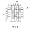
- FIG. 3 there is schematically shown an example of a cell 31 having a matrix electrode arrangement in which a ferroelectric liquid crystal compound (not shown) is interposed between a pair of groups of electrodes oppositely spaced from each other.
- Reference numerals 32 and 33 denote a group of scanning electrodes and a group of signal electrodes, respectively.
- a scanning electrode S 1 being selected is explained.
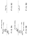
- FIGs 4A and 4B there are respectively shown electric signals applied to a selected scanning electrode S 1 and electric signals applied to the other scanning electrodes (non-selected scanning electrodes) S 2 , S 3 , S 4 .
- Figures 4C and 4D show electric signals applied to the selected signal electrode I 1 , I 3 , IS and electric signals applied to the non-selected signal electrodes I 2 , I4, respectively.
- the abscissa and the ordinate represent a time and a voltage, respectively. For instance, when displaying a motion picture, the group of scanning electrodes 32 are sequentially and periodically selected.
- a threshold voltage for giving a first stable state of the liquid crystal having bistability is referred to as V th1 and a threshold voltage for giving a second stable state thereof as -Vth2, respectively, at a specific voltage application time t 1 or t 2' an electric signal applied to the selects scanning electrode 42(S 1 ) is an alternating voltage showing 2V 0 at a phase (time) t 1 and -2V 0 at a phase (time) t 2 , as shown in Figure 4A.
- an electric signal having plural phases of mutually different voltages is applied to a selected scanning electrode, an important effect can be obtained that switching between the first and second stable states corresponding to optically "bright” and “dark” states, respectively, can be quickly caused.
- the other scanning electrodes S 2 - S 5 ... are grounded as shown in Figure 4B.
- the electric signals appearing thereon show zero volt.
- an electric signal applied to the selected signal electrodes I 1 , I3, 5 shows V as indicated in Figure 4C while an electric signal applied to the non-selected signal electrodes I 2 , I4 shows -V as indicated in Figure 7D.
- the voltage V is set to a desired value which satisfies V 0 ⁇ V th2 ⁇ 3V 0 and -3V 0 ⁇ -V th1 ⁇ -V 0 .
- a voltage applied to all the picture elements on the non-selected scanning lines is +V 0 or -V 0 , each not exceeding the threshold level. Accordingly, the ferroelectric liquid crystal molecules electrically connected to the respective picture elements on the non-selected scanning lines are placed in the orientations corresponding to signal states produced when they have been last scanned without change in orientation. Namely, when a certain scanning electrode is selected, signals corresponding to one line are written and thus writing of signals corresponding to one frame is completed. The signal state of each picture element can be maintained until the line is subsequently selected. Accordingly, even if the number of scanning lines increases, the duty ratio does not substantially change, resulting in no possibility of lowering in contrast, occurrence of crosstalk, etc.
- the liquid crystal layer is formed in an extremely thin layer as thin as 2 ⁇ m or less and accordingly a short circuit can be caused between the opposite electrodes through fine particles disposed in the device.
- a short circuit there is generally formed an insulating layer covering either one or both of the opposite electrodes, respectively.
- This additional voltage can cause reversal of display state from that obtained by writing in phase t 1 (first display state based on first orientation state of the ferroelectric liquid crystal) to the reverse display state (second display state based on second orientation state of the ferroelectric liquid crystal.
- phase t 1 first display state based on first orientation state of the ferroelectric liquid crystal
- second display state second display state based on second orientation state of the ferroelectric liquid crystal.
- Figure 7 shows time-serially applied waveforms by using unit pulse signal as shown in Figures 4A to 4D.
- a voltage of 3V a exceeding the threshold voltage V th2 is applied to a picture element A, whereby the picture element A is oriented or switched to one stable state, e.g., "bright" state, regardless of the previous history thereof.
- a voltage of -V 0 not exceeding the switching threshold voltage -V th1 is applied so that the picture element A retains "bright" state.
- Figure 8 is a graph plotting an application- time dependency of a threshold voltage required for switching when DOB AM BC (designated by reference numeral 82 in Figure 8) and HOBACPC (designated by reference numeral 81 in Figure 8) were used as ferroelectric liquid crystal materials.
- the thickness of the liquid crystal was 1.6 p, and the temperature was controlled at 70°C.
- the threshold voltages V th1 and T th2 were nearly equal to each other, i.e., V th1 ⁇ V t h2 ( ⁇ V th ).
- the threshold voltage V th has a dependency on the application time and becomes steeper according as an application time becomes shorter.
- some problem occurs when a driving method as practised in Figure 7 is employed, and when this driving method is applied to a device which has an extremely large number of scanning lines and is required to be driven at a high speed. Namely, for instance, even if the picture element A is switched to "bright" state at a time when the scanning electrode S is scanned, a voltage of -V is always and continuously applied after the concerned scanning is finished, whereby it is possible that the picture element is switched to the "dark" state before the scanning of one picture is completed.
- the voltage decrease ⁇ V 0 amounts to approximately 3V O /3, whereby a reversal of display occurs during one-frame period of writing operation as will be described in the examples appearing hereinafter.
- a ferroelectric liquid crystal having a volume resistivity of 1x10 9 ⁇ .cm or above it is conveniently adopted, for example, to add an adsorbent for ionic substances such as alumina particles, silica gel particles, etc. into a ferroelectric liquid crystal, vigorously stir the resultant mixture and separate the ionic adsorbent by filtration.
- the ionic adsorbent may preferably be in the form of particles having an average particle size of the order of 10 to 50 ⁇ m.
- volume resistivity of a ferroelectric liquid crystal material described herein has been obtained through the dual frequency method by using a circuit as shown in Figure 10 to apply rectangular pulses and using the following equations to calculate p (volume resistivity).
- V measured voltage
- f frequency of the rectangular pulses
- I C current of capacive component
- I R current of R component
- C capacitor of liquid crystal
- R resistivity of liquid crystal ( ⁇ ).
- p PS/d wherein d: thickness of liquid crystal layer (cell gap), and S: electrode area.
- the insulating material constituting the above mentioned insulating layer,used in the present invention are not particularly limited but may be appropriately be selected from inorganic insulating materials such as silicon nitride, silicon nitride containing hydrogen, silicon carbide, silicon carbide containing hydrogen, silicon oxide, boron nitride, boron nitride containing hydrogen, cerium oxide, aluminum oxide, zirconium oxide, titanium oxide and magnesium fluoride; or organic insulating materials such as polyvinyl alcohol, polyimide, polyamide-imide, polyester-imide, polyparaxylylene, polyester, polycarbonate, polyvinylacetal, polyvinyl chloride, polyvinyl acetate, polyamide, polystyrene, cellulose resin, melamine resin, urea resin, acrylic resin and photoresist resins.
- the insulating film may suitably be formed in a thickness
- ° ° of 5000 A or less preferably 100 to 5000 A, parti- cularly preferably 500 to 3000 A.
- the above mentioned reversal phenomenon may be prevented further more effectively by adjusting the capacitor of the insulating layer to 5.5 x 1 0 3 pF/cm 2 or above.
- the insulating layer preferably has a capacitor of 5.5 x 1 0 3 - 3.0 x 1 0 5 p F/ cm 2 , particularly preferably 9.0 x 10 3 - 5.5 x 1 0 4 p F/ cm 2 in order to provide a sufficient insulating property.
- DOBAMBC decyloxybenzylidene-p'-amino-2-methyl - butyl cinnamate
- a polarizer and an analyzer were disposed on both sides of the liquid crystal cell in a cross nicol relationship, and signals having waveforms as shown in Figures 4 and 5 were applied to the opposite matrix electrodes.
- the scanning signal was an alternating waveform of +8 volts and -8 volts as shown in Figure 4A, the writing signals were +4 volts and -4 volts, respectively, and the one-frame period was 30 m.sec.
- this liquid crystal device provided a normal motion picture display without causing reversal of written states.
- a liquid crystal device was prepared in the same manner as in the above except that the mechanical stirring of DOBAMBC in the presence of alumina particles was omitted.
- the volume resistivity of the liquid crystal in this device was measured in the same manner and formed to be 1.2 x 10 8 ⁇ .cm.
- a liquid crystal device was prepared in the same manner as in Example 1 except that the DOBAMBC used in Example 1 was replaced by HOBACPC (hexyloxy- benzylidene-p'-amino-2-chloropropyl cinnamate) prepared in Canon K.K.
- DOBAMBC DOBAMBC
- HOBACPC hexyloxy- benzylidene-p'-amino-2-chloropropyl cinnamate
- the volume resistivity of the liquid crystal cell was measured to be 1.6 x 10 10 ⁇ cm. After disposing a polarizer and an analyzer on the liquid crystal cell, the resultant liquid crystal was subjected to a time-division driving as described above, whereby good motion picture was displayed likewise.
- a liquid crystal device was prepared in the same manner as in the above Example 2 except that the mechanical stirring of HOBACPC in the presence of alumina particles was omitted.
- the volume resistivity of the liquid crystal in this device was measured in the same manner and formed to be 5.2 x 10⁸ ⁇ cm.
- the DOBAMBC and HOBACPC were subjected to mechanical stirring for different periods of time in the presence of alumina particles or to addition of an ionic surfactant to obtain ferroelectric liquid crystals having volume resistivities as shown in the following Table 1.
- Liquid crystal devices were prepared by using these ferroelectric liquid crystals and subjected to time-division driving in the same manner as in Example 1, whereby the results shown in Table 1 were obtained.
- the symbols used in Table 1 with respect to the display performance indicates the following. Thus, o shows that no reversal phenomenon was observed, x serious reversal phenomena observed, and partial reversal phenomena observed.
Abstract
Description
- The present invention relates to a liquid crystal device using a liquid crystal having bistability with respect to an electric field (hereinafter referred to as "bistable liquid crystal"), especially a ferroelectric liquid crystal, and more particularly to a liquid crystal device for time-division driving of the memory driving type.
- Liquid crystal display devices for displaying a pattern or information have been well known in which a plurality of scanning electrodes and a plurality of signal electrodes are arranged in the form of a matrix and liquid crystals are interposed between the scanning and signal electrodes, whereby a plurality of picture elements are defined. In order to drive such liquid crystal display devices, a time-division driving method is used in which an address signal is applied sequentially and periodically to the scanning electrodes and in synchronism with the address signal predetermined information signals are selectively applied to the signal electrodes in parallel. Such liquid crystal display devices and the methods for driving them have serious defects as will be described below.
- Thus, it is difficult to increase the density of picture elements or the size of a picture. Liquid crystals which have been used in practice in liquid crystal display device because of their fast response and their low electric power consumption are twisted nematic liquid crystals of the kind disclosed in, for instance, "Voltage Dependent Optical Activity of a Twisted Nematic Liquid Crystals", M. Schadt and W. Helfrich in Applied Physics Letters, Vol. 18, No. 4, (Feb. 15, 1971), pages 127 - 128. The liquid crystals of this kind assume a helical structure in which the molecules of a nematic liquid crystal having a positive dielectric anisotropy are twisted in the direction of the thickness of the liquid crystal layer and are arranged in parallel with each other between electrodes when it is not applied with an electric field. When an electric field is applied, the molecules of the nematic liquid crystal with a positive dielectric anisotropy are oriented or aligned in the direction of the electric field to cause optical modulation. In the case of a display device in which a liquid crystal of the kind described is used and which has a matrix of electrodes, a voltage higher than a threshold voltage required for arranging the molecules of the liquid crystal in the direction perpendicular to the surfaces of the electrodes is applied to a region (selected point) at which both a scanning electrode and a signal electrode are selected and no voltage is applied to a region (non-selected point) at which neither of a scanning electrode and a signal electrode is selected. As a result, the molecules of the liquid crystal are maintained in a stable state in which they are in parallel with the surfaces of the electrodes. When linear polarizers are disposed upon the upper and lower surfaces of a liquid crystal ceil or device of the type described in cross nicol relationship, a selected point prevents the transmission of light while a non-selected point permits the transmission of light, whereby a display or picture device is formed. However, in the case of a liquid crystal device with a matrix of electrodes, a finite electric field is applied to a region (the so-called "semi-selected or half-selected point") in which a scanning electrode,is selected while a signal electrode is not selected or in which a scanning electrode is not selected while a signal electrode is selected. When the difference between a voltage applied to a selected point and a voltage applied to a half-selected point is sufficiently large and if a threshold voltage at which the molecules of a liquid crystal are oriented in the direction perpendicular to an electric field applied is between the above described voltages, the correct operation of a display element can be ensured. However, when the number (N) of scanning lines is increased, a time period (duty ratio) during which one selected point is subjected to an effective electric field during the time when one frame is scanned is decreased at a ratio of 1/N. As a consequence, in the case of repetitive scanning, the greater the number of scanning lines, the smaller the effective voltage difference between a selected point and a non-selected point becomes. As a result, the problems of the reduction in contrast of a picture and of crosstalk are unavoidable. These essentially unavoidable problems result when a driving method (that is, a repetitive scanning method) in which a liquid crystal which is not bistable (that is, a liquid crystal in which the molecules assume a stable state in which they are oriented in the horizontal direction relative to the surfaces of the electrodes and are oriented in the vertical direction only when an effective electric field is applied) is driven by utilizing a time storage effect. In order to overcome these problems, there have been proposed a voltage averaging method, a two-frequency driving, a multiple matrix method and so on. However, neither of them is not satisfactory in solving the above described problems. Therefore, it is impossible at present to provide a display device with a large picture size and with a high density of picture elements because it is impossible to sufficiently increase the number of scanning lines.
- An object of the present invention is to provide a novel liquid crystal device for time-division driving which has solved the problems involved in the conventional liquid crystal devices.
- The liquid crystal device for time-division driving according to the present invention has been developed to accomplish the above object and more specifically comprises a liquid crystal device for time-division driving comprising a plurality of picture elements arranged in a plurality of rows; each picture element comprising opposite electrodes, a layer of a ferroelectric liquid crystal disposed between the opposite electrodes and placed under bistability condition, and an insulating layer disposed on at least one of the opposite electrodes, the liquid crystal device being adapted to driving according to a time-division driving scheme wherein a writing signal is applied row by row and cyclically to the picture elements, and a particular row of picture elements to which the writing signal has been applied in a writing cycle retain their written states until a writing signal is applied to the particular row in a subsequent writing cycle, the ferroelectric liquid crystal having a volume resistivity of 1x10⁹ Ω.cm or larger.
- These and other objects, features and advantages of the present invention will become more apparent upon a consideration of the following description of the preferred embodiments of the present invention taken in conjunction with the accomapnying drawings.
-
- Figures 1 and 2 are schematic perspective views illustrating the basic operation principle of the liquid crystal device for time division driving according to the present invention,
- Figure 3 is a plan view of a matrix electrode structure and picture elements formed at intersections of electrodes,
- Figures 4A to 4D illustrate electric signals applied to the matrix electrodes,
- Figures 5A to 5D illustrate voltage waveforms applied between matrix electrodes,
- Figure 6 shows a writing voltage waveform effectively applied to a liquid crystal layer at a picture element B,
- Figure 7 illustrates a time chart showing signals applied to the liquid crystal device according to the present invention,
- Figure 8 is a graph showing how a threshold voltage of a ferroelectric liquid crystal depends upon a voltage-application time,
- Figure 9 illustrates another embodiment of a time chart showing signals applied to the liquid crystal device according to the present invention, and
- Figure 10 shows a diagram of a circuit used for the volume resistivity of a liquid crystal.
- As the liquid crystal used in the liquid crystal - device according to the present invention, a liquid crystal material placed under a condition of assuming either a first optically stable state or a second optically stable state depending upon an electric field applied thereto, i.e., a bistable liquid crystal, is used.
- As such bistable liquid crystals, chiral smectic liquid crystals having ferroelectricity are most preferred. Among them, liquid crystals in chiral smectic C phase (SmC*), H phase (SmH*) , I phase (SmI*), J phase (SmJ*), K phase (SmK*), G phase (SmG*) or F phase (SmF*) are suited. These ferroelectric liquid crystals are described in, e.g., "LE JOURNAL DE PHYSIQUE LETTERS" 36 (L-69)-, 1975 "Ferroelectric Liquid Crystals": "Applied Physics Letters" 36 (11) 1980, "Submicro Second Bistable Electrooptic Switching in Liquid Crystals", "Solid State Physics" 16 (141), 1981 "Liquid Crystal", etc. Ferroelectric liquid crystals disclosed in these publications may be used in the present invention.
- Specific examples of the ferroelectric liquid crystal compounds to be used in the present invention include those represented by the following formulas (In the formulas, C accompanied with * is an asymmetric carbon atom.)


- When a device is constituted by using these materials, the device may be supported with a block of copper, etc., in which a heater is embedded in order to realize a temperature condition where the liquid crystal compounds assume a desired chiral smectic phase such as SmC*- or SmH*-phase.
- Referring to Figure 1, there is schematically shown an example of a ferroelectric liquid crystal cell. Reference numerals 11 and 11a denote base plates (glass plates) on which a transparent electrode of, e.g., In203, Sn02, ITO (Indium-Tin Oxide), etc., is disposed, respectively. A liquid crystal of an SmC*- phase in which liquid crystal
molecular layers 12 are oriented perpendicular to surfaces of the glass plates is hermetically disposed therebetween. Afull line 13 shows liquid crystal molecules. Eachliquid crystal molecule 13 has a dipole moment (P⊥) 14 in a direction perpendicular to the axis thereof. When a voltage higher than a certain threshold level is applied between electrodes formed on the base plates 11 and 11a, a helical structure of theliquid crystal molecule 13 is loosened to change the alignment direction of respectiveliquid crystal molecules 13 so that the dipole moments (P1) 14 are all directed in the direction of the electric field. Theliquid crystal molecules 13 have an elongated shape and show refractive anisotropy between the long axis and the short axis thereof. Accordingly, it is easily understood that when, for instance, polarizers arranged in a cross nicol relationship, i.e., with their polarizing directions crossing each other, are disposed on the upper and the lower surfaces of the glass plates, the liquid crystal cell thus arranged functions as a liquid crystal optical modulation device of which optical characteristics vary depending upon the polarity of an applied voltage. Further, when the thickness of the liquid crystal cell is sufficiently thin (e.g., 1 u), the helical structure of the liquid crystal molecules is loosened without application of an electric field whereby the dipole moment assumes either of the two states, i.e., P in anupper direction 24 or Pa in alower direction 24a, thus providing a bistability condition, as shown in Figure 2. When an electric field E or Ea higher than a certain threshold level and different from each other in polarity as shown in Figure 2 is applied to a cell having the above-mentioned characteristics, the dipole moment is directed either in theupper direction 24 or in thelower direction 24a depending on the vector of the electric field E or Ea. In correspondence with this, the liquid crystal molecules are oriented to either a firststable state 23 or a secondstable state 23a. - When the above-mentioned ferroelectric liquid crystal is used as an optical modulation element, it is possible to obtain two advantages. First is that the response speed is quite fast. Second is that the orientation of the liquid crystal shows bistability. The second advantage will be further explained, e.g., with reference to Figure 2. When the electric field E is applied to the liquid crystal molecules, they are oriented in the first
stable state 23. This state is stably retained even if the electric field is removed. On the other hand, when the electric field Ea of which direction is opposite to that of the electric field E is applied thereto, the liquid crystal molecules are oriented to the secondstable state 23a, whereby the directions of molecules are changed. Likewise, the latter state is stably retained even if the electric field is removed. Further, as long as the magnitude of the electric field E being applied is not above a certain threshold value, the liquid crystal molecules are placed in the respective orientation states. In order to effectively realize high response speed and bistability, it is preferable that the thickness of the cell is as thin as possible and generally 0.5 to 20 µ, particularly 2 p or less. A liquid crystal electro- optical device having a matrix electrode structure in which the ferroelectric liquid crystal of this kind is used is proposed, e.g., in the specification of U.S. Patent No. 4367924 by Clark and Lagerwall. - Next, an embodiment of method for driving a ferroelectric liquid crystal will be described with reference to Figures 3 to 5.
- Referring to Figure 3, there is schematically shown an example of a
cell 31 having a matrix electrode arrangement in which a ferroelectric liquid crystal compound (not shown) is interposed between a pair of groups of electrodes oppositely spaced from each other.Reference numerals electrodes 32 are sequentially and periodically selected. If a threshold voltage for giving a first stable state of the liquid crystal having bistability is referred to as Vth1 and a threshold voltage for giving a second stable state thereof as -Vth2, respectively, at a specific voltage application time t1 or t2' an electric signal applied to the selects scanning electrode 42(S1) is an alternating voltage showing 2V0 at a phase (time) t1 and -2V0 at a phase (time) t2, as shown in Figure 4A. When such an electric signal having plural phases of mutually different voltages is applied to a selected scanning electrode, an important effect can be obtained that switching between the first and second stable states corresponding to optically "bright" and "dark" states, respectively, can be quickly caused. - On the other hand, the other scanning electrodes S2 - S5 ... are grounded as shown in Figure 4B. Accord-. ingly, the electric signals appearing thereon show zero volt. Further, an electric signal applied to the selected signal electrodes I1, I3, 5 shows V as indicated in Figure 4C while an electric signal applied to the non-selected signal electrodes I2, I4 shows -V as indicated in Figure 7D. In this instance, the voltage V is set to a desired value which satisfies V0 < V th2 < 3V0 and -3V0 < -Vth1 < -V0. Voltage waveforms applied to each picture elements A and B, for example, among the picture elements shown in Figure 3, when such electric signals are given are shown in Figures 5A and 5B, respectively. Namely, as seen from Figure 5A, a first signal voltage of 3V0 above the threshold level Vth2 is applied to the ferroelectric liquid crystal at the picture elements A on the selected scanning line at a phase t2. Further, a second signal voltage of -3V0 exceeding the threshold level -Vth1 is applied to the ferroelectric liquid crystal at the picture elements B on the same scanning line at a phase t1. Accordingly, depending upon whether a signal electrode is selected or not on a selected scanning electrode line, the orientation of liquid crystal molecules changes. Thus, when a certain signal electrode is selected, the liquid crystal molecules are oriented to the first stable state, while when not selected, oriented to the second stable state. In either case, the orientation of the liquid crystal molecules is not related to the previous states of each picture element.
- On the other hand, as shown in Figures 5C and 5D, a voltage applied to all the picture elements on the non-selected scanning lines is +V0 or -V0, each not exceeding the threshold level. Accordingly, the ferroelectric liquid crystal molecules electrically connected to the respective picture elements on the non-selected scanning lines are placed in the orientations corresponding to signal states produced when they have been last scanned without change in orientation. Namely, when a certain scanning electrode is selected, signals corresponding to one line are written and thus writing of signals corresponding to one frame is completed. The signal state of each picture element can be maintained until the line is subsequently selected. Accordingly, even if the number of scanning lines increases, the duty ratio does not substantially change, resulting in no possibility of lowering in contrast, occurrence of crosstalk, etc.
- Referring to Figure 3, it is assumed that, among the picture elements formed at intersections of the scanning electrodes S, - S5 ... and the signal electrodes I1 - I5, the picture elements with hatching are in the "bright" state and picture elements drawn in white are in the "dark" state. When display states on a signal electrode I1 in Figure 9 are noted, a picture element (A) on a scanning electrode S1 is in the "bright" state, and the other picture elements (B) are all in the dark state.
- By the way, with respect to a ferroelectric liquid crystal device placed under bistability condition as described above, the liquid crystal layer is formed in an extremely thin layer as thin as 2 µm or less and accordingly a short circuit can be caused between the opposite electrodes through fine particles disposed in the device. In order to obviate the short circuit, there is generally formed an insulating layer covering either one or both of the opposite electrodes, respectively.
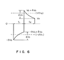
- However, because of the insulating layer(s) formed on the opposite electrodes, when a writing pulse as shown in Figure 5B, which is expected to be sufficiently large to cause complete reversal of the ferroelectric liquid crystal, is applied to, e.g., a picture element B between the electrodes, a voltage having a waveform as shown in Figure 6 is actually applied to the liquid crystal layer. Thus, the actual voltage decreases in absolute value from -3V0 by ΔV0 in a proportion of π = R1 (C1+C2) (wherein R1: resistivity of the liquid crystal layer, C1: capacitance of a unit area of the liquid crystal layer, C2: capacitance of a unit area of the dielectric layer), and the decreased voltage AV0 is added to Va which is expected to be applied at the time of switching of pulses, i.e., at the beginning of phase t2. This additional voltage can cause reversal of display state from that obtained by writing in phase t1 (first display state based on first orientation state of the ferroelectric liquid crystal) to the reverse display state (second display state based on second orientation state of the ferroelectric liquid crystal. The above fact has been clarified by our experiments. More specifically, in a line-by-line writing scheme as explained with reference to the figures 4A to 5D, a display state obtained in phase t is required to be retained without reversal in phase t2. Thus, a voltage exceeding a reversal or switching threshold voltage must not be applied in phase t2' According to out study, however, it has been clarified that a voltage V0 + AV0 exceeding the switching threshold voltage is applied in phase t2 at the time of switching pulse polarities from phase t1 to phase t2 and a picture element expected to retain the first display state is reversed to the second display state, whereby a desired display cannot be attained. It has been also clarified that this phenomenon is caused by a reverse electric field (+ΔV0) generated by discharge from the capacitor of the dielectric layer connected in series to the liquid crystal layer at the time of switching pulse polarities.
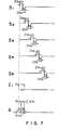
- On the other hand, it has also been recognized that a picture element which has been written in the first or second display state in phases t1 and t2 can reverse the display state even in a non-scanning time period because information signals are continually applied from data lines. In order to obviate this problem, a method of applying alternating voltages not exceeding threshold values to the picture elements after writing has been conceived. A mode of operation according to this method is illustrated in Figure 9 wherein a writing signal and auxiliary signals of alternating voltages for preventing reversal phenomena, which are applied to a picture element A, are shown in time series by way of waveforms. However, application of such alternating voltages (e.g., AC voltages) also involve the problem as described above caused by the addition of a reverse electric field accompanying the application of reverse polarities of pulses as shown in the waveform at the bottom of Figure 9.
- Further, Figure 7 shows time-serially applied waveforms by using unit pulse signal as shown in Figures 4A to 4D. Referring to Figure 7, according to an ideal operation, a voltage of 3Va exceeding the threshold voltage Vth2 is applied to a picture element A, whereby the picture element A is oriented or switched to one stable state, e.g., "bright" state, regardless of the previous history thereof. Thereafter, while the other scanning lines S2 - s5 ... are scanned, a voltage of -V0 not exceeding the switching threshold voltage -Vth1 is applied so that the picture element A retains "bright" state. In actual operations, however, when one direction of signal (one for providing "dark" state in this case) is continually applied to one signal electrode in this manner, a problem can occur especially in a case where a very large number of scanning lines are used and a high speed driving is pursued. This is explained based on some experimental data.
- Figure 8 is a graph plotting an application- time dependency of a threshold voltage required for switching when DOBAMBC (designated by reference numeral 82 in Figure 8) and HOBACPC (designated by reference numeral 81 in Figure 8) were used as ferroelectric liquid crystal materials. In both cases, the thickness of the liquid crystal was 1.6 p, and the temperature was controlled at 70°C. In this experiment, as base plates between which a liquid crystal was hermetically interposed, e.g., glass plates on which ITO was vapor-deposited were used, and the threshold voltages Vth1 and Tth2 were nearly equal to each other, i.e., Vth1≈ Vth2 (≡Vth).
- As seen from Figure 8, it is understood that the threshold voltage Vth has a dependency on the application time and becomes steeper according as an application time becomes shorter. As will be understood from the above-mentioned consideration, some problem occurs when a driving method as practised in Figure 7 is employed, and when this driving method is applied to a device which has an extremely large number of scanning lines and is required to be driven at a high speed. Namely, for instance, even if the picture element A is switched to "bright" state at a time when the scanning electrode S is scanned, a voltage of -V is always and continuously applied after the concerned scanning is finished, whereby it is possible that the picture element is switched to the "dark" state before the scanning of one picture is completed.
- Particularly, where an insulating layer is formed on an electrode, the effective voltage decreases with the lapse of time since the time of pulse application, the thus decreased voltage is added as a reverse polarity of voltage at the time of switching pulses. This phenomenon is illustrated at the bottom of Figure 7. Thus, in view of the waveform A in Figure 7, at voltage of 3V0 is not applied in phase t2 but a voltage decrease of AVO gradually occurs. When this writing signal is ceased to be applied, an additional voltage of -V0 is applied whereby the above mentioned reversal phenomenon is accelerated.
- As a result of our further study, based on the above observation, especially on the bistable liquid crystal constituting a liquid crystal device, it has been found possible to prevent the above mentioned reversal phenomenon and retain a once-written signal state until the subsequent writing cycle when the volume resistivity of the ferroelectric liquid crystal is adjusted to 1x10⁹ Ω.cm or above, more specifically to a range of 1x10 9 Ω.cm to
1x 10¹³ Ω.cm, preferably 1x10¹⁰ Ω.cm to 1x10¹³ Ω.cm and particularly preferably to a range of 1x10¹¹Ω·cm to 1x10 13 Ω.cm. - On the other hand, if the volume resistivity of the ferroelectric liquid crystal is below 1x10⁹ Ω.cm, the voltage decrease ΔV0 amounts to approximately 3VO/3, whereby a reversal of display occurs during one-frame period of writing operation as will be described in the examples appearing hereinafter.
- In order to obtain a ferroelectric liquid crystal having a volume resistivity of 1x10⁹ Ω.cm or above, it is conveniently adopted, for example, to add an adsorbent for ionic substances such as alumina particles, silica gel particles, etc. into a ferroelectric liquid crystal, vigorously stir the resultant mixture and separate the ionic adsorbent by filtration. The ionic adsorbent may preferably be in the form of particles having an average particle size of the order of 10 to 50 µm.
- The "volume resistivity" of a ferroelectric liquid crystal material described herein has been obtained through the dual frequency method by using a circuit as shown in Figure 10 to apply rectangular pulses and using the following equations to calculate p (volume resistivity).

- For different frequencies, the following equations are used:


- Finally, p is calculated by the following equation: p = PS/d
wherein d: thickness of liquid crystal layer (cell gap), and S: electrode area. - The insulating material constituting the above mentioned insulating layer,used in the present invention are not particularly limited but may be appropriately be selected from inorganic insulating materials such as silicon nitride, silicon nitride containing hydrogen, silicon carbide, silicon carbide containing hydrogen, silicon oxide, boron nitride, boron nitride containing hydrogen, cerium oxide, aluminum oxide, zirconium oxide, titanium oxide and magnesium fluoride; or organic insulating materials such as polyvinyl alcohol, polyimide, polyamide-imide, polyester-imide, polyparaxylylene, polyester, polycarbonate, polyvinylacetal, polyvinyl chloride, polyvinyl acetate, polyamide, polystyrene, cellulose resin, melamine resin, urea resin, acrylic resin and photoresist resins. The insulating film may suitably be formed in a thickness
- ° ° of 5000 A or less, preferably 100 to 5000 A, parti- cularly preferably 500 to 3000 A.
- The above mentioned reversal phenomenon may be prevented further more effectively by adjusting the capacitor of the insulating layer to 5.5 x 10³ pF/cm2 or above. The insulating layer preferably has a capacitor of 5.5 x 10³ - 3.0 x 10⁵ pF/cm2, particularly preferably 9.0 x 10³ - 5.5 x 10⁴ pF/cm2 in order to provide a sufficient insulating property.
- The present invention will be explained in further detail by way of actual examples of production.
- On two electrode plates with stripe-form electrodes designed to cross each other to form opposite matrix electrodes, a 5 wt.% solution of a polyamic acid resin (combined product of pyromellitic anhydride and 4,4'-diaminodiphenyl ether) in N-methylpyrrolidone was applied and heated to 250°C to cause ring-closure reaction to form a 1000 A-thick polyimide film. The polyimide films on the two electrodes were respectively rubbed in one direction, and the electrode plates were fixed to each other so that their rubbed directions were in parallel with each other to form a cell.
- Then, 0.3 wt. part of alumina particles having an average particle size of 30 µ was added to 1 wt. part of DOBAMBC (decyloxybenzylidene-p'-amino-2-methyl- butyl cinnamate) prepared in Canon Kabushiki Kaisha., and the mixture was mechanically stirred for 2 hours at a temperature providing the isotropic phase of DOBAMBC. After the mechanical stirring, DOBAMBC was separated by filtration and injected by the vacuum injection method and sealed up in the above prepared cell while being in the isotropic phase. Then, the cell was gradually cooled at a rate of 5°C/hour to form a liquid crystal cell of SmC*. A voltage of 10 V was applied to the liquid crystal cell at frequencies of 32 Hz and 64 Hz, respectively, to measure the electric current values, from which the volume resistivity of the liquid crystal was calculated at 3.7 x 10⁹ Ω•cm.
- A polarizer and an analyzer were disposed on both sides of the liquid crystal cell in a cross nicol relationship, and signals having waveforms as shown in Figures 4 and 5 were applied to the opposite matrix electrodes. The scanning signal was an alternating waveform of +8 volts and -8 volts as shown in Figure 4A, the writing signals were +4 volts and -4 volts, respectively, and the one-frame period was 30 m.sec.
- As a result of the memory-drive type time-division driving operation as described hereinbefore under these conditions, this liquid crystal device provided a normal motion picture display without causing reversal of written states.
- On the other hand, as a comparative test, a liquid crystal device was prepared in the same manner as in the above except that the mechanical stirring of DOBAMBC in the presence of alumina particles was omitted. The volume resistivity of the liquid crystal in this device was measured in the same manner and formed to be 1.2 x 10⁸ Ω.cm. When this liquid crystal device was driven in the same manner as described above, a once-written display state was reversed during one-frame operation whereby normal motion picture was not displayed.
- A liquid crystal device was prepared in the same manner as in Example 1 except that the DOBAMBC used in Example 1 was replaced by HOBACPC (hexyloxy- benzylidene-p'-amino-2-chloropropyl cinnamate) prepared in Canon K.K.
- The volume resistivity of the liquid crystal cell was measured to be 1.6 x 10¹⁰ Ω·cm. After disposing a polarizer and an analyzer on the liquid crystal cell, the resultant liquid crystal was subjected to a time-division driving as described above, whereby good motion picture was displayed likewise.
- A liquid crystal device was prepared in the same manner as in the above Example 2 except that the mechanical stirring of HOBACPC in the presence of alumina particles was omitted. The volume resistivity of the liquid crystal in this device was measured in the same manner and formed to be 5.2 x 10⁸ Ω·cm. When this liquid crystal device was driven in the same manner as described above, a once-written display state was reversed during one-frame operation whereby normal motion picture was not displayed.
- The DOBAMBC and HOBACPC were subjected to mechanical stirring for different periods of time in the presence of alumina particles or to addition of an ionic surfactant to obtain ferroelectric liquid crystals having volume resistivities as shown in the following Table 1.
- Liquid crystal devices were prepared by using these ferroelectric liquid crystals and subjected to time-division driving in the same manner as in Example 1, whereby the results shown in Table 1 were obtained. The symbols used in Table 1 with respect to the display performance indicates the following. Thus, o shows that no reversal phenomenon was observed, x serious reversal phenomena observed, and partial reversal phenomena observed.

Claims (26)
Applications Claiming Priority (2)
| Application Number | Priority Date | Filing Date | Title |
|---|---|---|---|
| JP59209255A JPS6186732A (en) | 1984-10-04 | 1984-10-04 | Liquid crystal element for time division drive |
| JP209255/84 | 1984-10-04 |
Publications (3)
| Publication Number | Publication Date |
|---|---|
| EP0177365A2 true EP0177365A2 (en) | 1986-04-09 |
| EP0177365A3 EP0177365A3 (en) | 1987-01-21 |
| EP0177365B1 EP0177365B1 (en) | 1991-07-24 |
Family
ID=16569924
Family Applications (1)
| Application Number | Title | Priority Date | Filing Date |
|---|---|---|---|
| EP85307125A Expired - Lifetime EP0177365B1 (en) | 1984-10-04 | 1985-10-04 | Liquid crystal device for time-division driving |
Country Status (4)
| Country | Link |
|---|---|
| US (1) | US4681404A (en) |
| EP (1) | EP0177365B1 (en) |
| JP (1) | JPS6186732A (en) |
| DE (1) | DE3583570D1 (en) |
Cited By (5)
| Publication number | Priority date | Publication date | Assignee | Title |
|---|---|---|---|---|
| EP0247806A2 (en) * | 1986-05-27 | 1987-12-02 | Seiko Instruments Inc. | Method for driving a ferroelectric liquid crystal electro-optical device |
| EP0281160A1 (en) * | 1987-03-05 | 1988-09-07 | Canon Kabushiki Kaisha | Liquid crystal apparatus |
| EP0285402A2 (en) * | 1987-03-31 | 1988-10-05 | Canon Kabushiki Kaisha | Display device |
| EP0285401A2 (en) * | 1987-03-31 | 1988-10-05 | Canon Kabushiki Kaisha | Display device |
| US4917470A (en) * | 1985-01-14 | 1990-04-17 | Canon Kabushiki Kaisha | Driving method for liquid crystal cell and liquid crystal apparatus |
Families Citing this family (47)
| Publication number | Priority date | Publication date | Assignee | Title |
|---|---|---|---|---|
| US4979805A (en) * | 1984-07-23 | 1990-12-25 | Canon Kabushiki Kaisha | Ferroelectric liquid crystal device containing optically active azo or azoxy benzene type mesomorphic compound with extended life |
| JPS6236488A (en) * | 1985-08-11 | 1987-02-17 | Semiconductor Energy Lab Co Ltd | Liquid crystal display |
| JPH0690375B2 (en) * | 1986-04-17 | 1994-11-14 | キヤノン株式会社 | Liquid crystal device |
| JP2505757B2 (en) * | 1986-07-23 | 1996-06-12 | キヤノン株式会社 | Driving method of optical modulator |
| JPH0833560B2 (en) * | 1986-11-27 | 1996-03-29 | キヤノン株式会社 | Liquid crystal element |
| US5285214A (en) * | 1987-08-12 | 1994-02-08 | The General Electric Company, P.L.C. | Apparatus and method for driving a ferroelectric liquid crystal device |
| JP2770944B2 (en) * | 1987-08-19 | 1998-07-02 | キヤノン株式会社 | Liquid crystal element |
| US4857906A (en) * | 1987-10-08 | 1989-08-15 | Tektronix, Inc. | Complex waveform multiplexer for liquid crystal displays |
| DE3856474T2 (en) * | 1987-11-12 | 2001-11-08 | Canon Kk | Liquid crystal device |
| GB8726996D0 (en) * | 1987-11-18 | 1987-12-23 | Secr Defence | Multiplex addressing of ferro-electric liquid crystal displays |
| JP2655719B2 (en) * | 1989-03-20 | 1997-09-24 | 富士通株式会社 | Liquid crystal display device |
| JP2769879B2 (en) * | 1989-09-29 | 1998-06-25 | キヤノン株式会社 | Chiral smectic liquid crystal device |
| CA2038687C (en) * | 1990-03-22 | 1996-05-07 | Shuzo Kaneko | Method and apparatus for driving active matrix liquid crystal device |
| JP2915104B2 (en) * | 1990-07-30 | 1999-07-05 | キヤノン株式会社 | Liquid crystal element and liquid crystal driving method |
| JP2775527B2 (en) * | 1991-02-01 | 1998-07-16 | キヤノン株式会社 | Chiral smectic liquid crystal device |
| JPH04258924A (en) * | 1991-02-13 | 1992-09-14 | Canon Inc | Ferroelectric liquid crystal element |
| JPH05150244A (en) * | 1991-02-20 | 1993-06-18 | Canon Inc | Ferroelectric liquid crystal element |
| US5420603A (en) * | 1991-02-20 | 1995-05-30 | Canon Kabushiki Kaisha | Display apparatus |
| JP2826776B2 (en) * | 1991-02-20 | 1998-11-18 | キヤノン株式会社 | Ferroelectric liquid crystal device |
| JP2835787B2 (en) * | 1991-03-22 | 1998-12-14 | キヤノン株式会社 | Ferroelectric liquid crystal device |
| JP2737032B2 (en) * | 1991-03-28 | 1998-04-08 | キヤノン株式会社 | Liquid crystal cell |
| JP2794226B2 (en) * | 1991-04-15 | 1998-09-03 | キヤノン株式会社 | Driving device and driving method for ferroelectric liquid crystal device |
| EP0509490A3 (en) * | 1991-04-16 | 1993-05-26 | Canon Kabushiki Kaisha | Liquid crystal apparatus |
| JP2847331B2 (en) * | 1991-04-23 | 1999-01-20 | キヤノン株式会社 | Liquid crystal display |
| JP2938232B2 (en) * | 1991-07-25 | 1999-08-23 | キヤノン株式会社 | Ferroelectric liquid crystal display device |
| JPH05224625A (en) * | 1992-02-12 | 1993-09-03 | Nec Corp | Driving method for liquid crystal display device |
| JP2563720B2 (en) * | 1992-03-30 | 1996-12-18 | 松下電器産業株式会社 | Ferroelectric liquid crystal panel |
| EP0564263B1 (en) * | 1992-04-01 | 1998-09-30 | Canon Kabushiki Kaisha | Display apparatus |
| US5552911A (en) * | 1992-10-19 | 1996-09-03 | Canon Kabushiki Kaisha | Color liquid crystal display device having varying cell thickness and varying pixel areas |
| US5657038A (en) * | 1992-12-21 | 1997-08-12 | Canon Kabushiki Kaisha | Liquid crystal display apparatus having substantially the same average amount of transmitted light after white reset as after black reset |
| KR950011959B1 (en) * | 1992-12-24 | 1995-10-12 | 엘지전자주식회사 | Liquid crystal injecting method |
| JP3118682B2 (en) * | 1992-12-25 | 2000-12-18 | キヤノン株式会社 | Liquid crystal display |
| JP2759589B2 (en) * | 1992-12-28 | 1998-05-28 | キヤノン株式会社 | Ferroelectric liquid crystal display device |
| DE69317640T2 (en) * | 1992-12-28 | 1998-07-30 | Canon Kk | Method and device for a liquid crystal display |
| US5471229A (en) * | 1993-02-10 | 1995-11-28 | Canon Kabushiki Kaisha | Driving method for liquid crystal device |
| US5539553A (en) * | 1993-04-09 | 1996-07-23 | Canon Kabushiki Kaisha | Liquid crystal device with an electrically neutral interface between the liquid crystal and orientation layer |
| US5532713A (en) * | 1993-04-20 | 1996-07-02 | Canon Kabushiki Kaisha | Driving method for liquid crystal device |
| US5592190A (en) * | 1993-04-28 | 1997-01-07 | Canon Kabushiki Kaisha | Liquid crystal display apparatus and drive method |
| JP3093627B2 (en) * | 1996-02-09 | 2000-10-03 | キヤノン株式会社 | Manufacturing method of liquid crystal display device |
| US5973761A (en) * | 1997-01-31 | 1999-10-26 | Canon Kabushiki Kaisha | Ferroelectic liquid crystal device having a low-resistivity layer below an alignment control layer |
| US20010052885A1 (en) * | 1997-09-12 | 2001-12-20 | Masaya Okita | Method for driving a nematic liquid crystal |
| JPH11296150A (en) | 1998-04-10 | 1999-10-29 | Masaya Okita | High-speed driving method for liquid crystal |
| GB2394781B (en) * | 2002-10-31 | 2005-11-09 | Hewlett Packard Co | Bistable nematic liquid crystal display device |
| GB2424716B (en) * | 2005-03-29 | 2010-03-24 | Hewlett Packard Development Co | Bistable liquid crystal display device |
| JP5495003B2 (en) * | 2008-04-11 | 2014-05-21 | Dic株式会社 | Ferroelectric liquid crystal composition and display device using the same |
| US20110298767A1 (en) * | 2010-06-04 | 2011-12-08 | O'callaghan Mike | Liquid crystal displays |
| US9562191B2 (en) * | 2015-04-01 | 2017-02-07 | Citizen Finedevice Co., Ltd. | Compositions and methods for removing ions from liquid crystal materials |
Citations (4)
| Publication number | Priority date | Publication date | Assignee | Title |
|---|---|---|---|---|
| EP0092181A2 (en) * | 1982-04-16 | 1983-10-26 | Hitachi, Ltd. | Method for driving liquid crystal element employing ferroelectric liquid crystal |
| EP0106386A2 (en) * | 1982-09-23 | 1984-04-25 | BBC Brown Boveri AG | Method of triggering a multiplexable bistable liquid crystal display |
| DE3414704A1 (en) * | 1983-04-19 | 1984-10-25 | Canon K.K., Tokio/Tokyo | METHOD FOR DRIVING AN OPTICAL MODULATING DEVICE |
| EP0149899A2 (en) * | 1983-12-09 | 1985-07-31 | Seiko Instruments Inc. | A liquid crystal display device |
Family Cites Families (6)
| Publication number | Priority date | Publication date | Assignee | Title |
|---|---|---|---|---|
| US3861135A (en) * | 1973-02-08 | 1975-01-21 | Chomerics Inc | Electrical interconnector and method of making |
| US4538884A (en) * | 1981-07-10 | 1985-09-03 | Canon Kabushiki Kaisha | Electro-optical device and method of operating same |
| US4595260A (en) * | 1982-05-28 | 1986-06-17 | Nec Corporation | Liquid crystal projection display with even temperature elevation |
| JPS59131910A (en) * | 1983-01-18 | 1984-07-28 | Seiko Epson Corp | Imaging device |
| JPS59131913A (en) * | 1983-01-19 | 1984-07-28 | Seiko Epson Corp | Liquid crystal electrooptic device |
| JPS59201021A (en) * | 1983-04-28 | 1984-11-14 | Canon Inc | Optical modulation element and its manufacture |
-
1984
- 1984-10-04 JP JP59209255A patent/JPS6186732A/en active Granted
-
1985
- 1985-09-24 US US06/779,651 patent/US4681404A/en not_active Expired - Lifetime
- 1985-10-04 EP EP85307125A patent/EP0177365B1/en not_active Expired - Lifetime
- 1985-10-04 DE DE8585307125T patent/DE3583570D1/en not_active Expired - Lifetime
Patent Citations (4)
| Publication number | Priority date | Publication date | Assignee | Title |
|---|---|---|---|---|
| EP0092181A2 (en) * | 1982-04-16 | 1983-10-26 | Hitachi, Ltd. | Method for driving liquid crystal element employing ferroelectric liquid crystal |
| EP0106386A2 (en) * | 1982-09-23 | 1984-04-25 | BBC Brown Boveri AG | Method of triggering a multiplexable bistable liquid crystal display |
| DE3414704A1 (en) * | 1983-04-19 | 1984-10-25 | Canon K.K., Tokio/Tokyo | METHOD FOR DRIVING AN OPTICAL MODULATING DEVICE |
| EP0149899A2 (en) * | 1983-12-09 | 1985-07-31 | Seiko Instruments Inc. | A liquid crystal display device |
Cited By (10)
| Publication number | Priority date | Publication date | Assignee | Title |
|---|---|---|---|---|
| US4917470A (en) * | 1985-01-14 | 1990-04-17 | Canon Kabushiki Kaisha | Driving method for liquid crystal cell and liquid crystal apparatus |
| EP0247806A2 (en) * | 1986-05-27 | 1987-12-02 | Seiko Instruments Inc. | Method for driving a ferroelectric liquid crystal electro-optical device |
| EP0247806A3 (en) * | 1986-05-27 | 1990-08-22 | Seiko Instruments Inc. | A ferroelectric liquid crystal electro-optical device |
| EP0281160A1 (en) * | 1987-03-05 | 1988-09-07 | Canon Kabushiki Kaisha | Liquid crystal apparatus |
| US5182549A (en) * | 1987-03-05 | 1993-01-26 | Canon Kabushiki Kaisha | Liquid crystal apparatus |
| US6046717A (en) * | 1987-03-05 | 2000-04-04 | Canon Kabushiki Kaisha | Liquid crystal apparatus |
| EP0285402A2 (en) * | 1987-03-31 | 1988-10-05 | Canon Kabushiki Kaisha | Display device |
| EP0285401A2 (en) * | 1987-03-31 | 1988-10-05 | Canon Kabushiki Kaisha | Display device |
| EP0285402A3 (en) * | 1987-03-31 | 1990-07-04 | Canon Kabushiki Kaisha | Display device |
| EP0285401A3 (en) * | 1987-03-31 | 1990-07-18 | Canon Kabushiki Kaisha | Display device |
Also Published As
| Publication number | Publication date |
|---|---|
| DE3583570D1 (en) | 1991-08-29 |
| EP0177365A3 (en) | 1987-01-21 |
| JPS6186732A (en) | 1986-05-02 |
| JPH0120725B2 (en) | 1989-04-18 |
| US4681404A (en) | 1987-07-21 |
| EP0177365B1 (en) | 1991-07-24 |
Similar Documents
| Publication | Publication Date | Title |
|---|---|---|
| EP0177365B1 (en) | Liquid crystal device for time-division driving | |
| US4738515A (en) | Driving method for liquid crystal device | |
| US4714323A (en) | Ferroelectric liquid crystal device having chiral smectic and nematic liquid crystal composition | |
| US5488388A (en) | Liquid crystal apparatus | |
| US5092665A (en) | Driving method for ferroelectric liquid crystal optical modulation device using an auxiliary signal to prevent inversion | |
| US4800382A (en) | Driving method for liquid crystal device | |
| US5559616A (en) | Driving method for ferroelectric liquid crystal device with partial erasure and partial writing | |
| JPH0422496B2 (en) | ||
| US4917470A (en) | Driving method for liquid crystal cell and liquid crystal apparatus | |
| EP0350934B1 (en) | Liquid crystal apparatus | |
| US5136408A (en) | Liquid crystal apparatus and driving method therefor | |
| US5724059A (en) | Method for driving optical modulation device | |
| US6351256B1 (en) | Addressing method and apparatus | |
| JPS6033535A (en) | Driving method of optical modulating element | |
| JPH079508B2 (en) | Liquid crystal display device and driving method thereof | |
| CA1317386C (en) | Ferroelectric liquid crystal device | |
| EP0344753B1 (en) | Liquid crystal apparatus and driving method therefor | |
| JPS61243430A (en) | Driving method for ferroelectric liquid crystal element | |
| JP2584752B2 (en) | Liquid crystal device | |
| JP2525453B2 (en) | Liquid crystal device and driving method thereof | |
| JP2584214B2 (en) | Driving method of liquid crystal element | |
| JPS61235897A (en) | Driving of liquid crystal element | |
| JPS62184437A (en) | Method for driving optical modulating element | |
| US5757350A (en) | Driving method for optical modulation device | |
| JPH1054976A (en) | Liquid crystal display device, circuit and method for driving it |
Legal Events
| Date | Code | Title | Description |
|---|---|---|---|
| PUAI | Public reference made under article 153(3) epc to a published international application that has entered the european phase |
Free format text: ORIGINAL CODE: 0009012 |
|
| AK | Designated contracting states |
Kind code of ref document: A2 Designated state(s): CH DE FR GB LI NL |
|
| PUAL | Search report despatched |
Free format text: ORIGINAL CODE: 0009013 |
|
| AK | Designated contracting states |
Kind code of ref document: A3 Designated state(s): CH DE FR GB LI NL |
|
| 17P | Request for examination filed |
Effective date: 19870610 |
|
| 17Q | First examination report despatched |
Effective date: 19890425 |
|
| GRAA | (expected) grant |
Free format text: ORIGINAL CODE: 0009210 |
|
| AK | Designated contracting states |
Kind code of ref document: B1 Designated state(s): CH DE FR GB LI NL |
|
| REF | Corresponds to: |
Ref document number: 3583570 Country of ref document: DE Date of ref document: 19910829 |
|
| ET | Fr: translation filed | ||
| PLBE | No opposition filed within time limit |
Free format text: ORIGINAL CODE: 0009261 |
|
| STAA | Information on the status of an ep patent application or granted ep patent |
Free format text: STATUS: NO OPPOSITION FILED WITHIN TIME LIMIT |
|
| 26N | No opposition filed | ||
| REG | Reference to a national code |
Ref country code: GB Ref legal event code: IF02 |
|
| PGFP | Annual fee paid to national office [announced via postgrant information from national office to epo] |
Ref country code: GB Payment date: 20020920 Year of fee payment: 18 |
|
| PGFP | Annual fee paid to national office [announced via postgrant information from national office to epo] |
Ref country code: CH Payment date: 20021016 Year of fee payment: 18 |
|
| PGFP | Annual fee paid to national office [announced via postgrant information from national office to epo] |
Ref country code: FR Payment date: 20021021 Year of fee payment: 18 |
|
| PGFP | Annual fee paid to national office [announced via postgrant information from national office to epo] |
Ref country code: NL Payment date: 20021031 Year of fee payment: 18 |
|
| PG25 | Lapsed in a contracting state [announced via postgrant information from national office to epo] |
Ref country code: GB Free format text: LAPSE BECAUSE OF NON-PAYMENT OF DUE FEES Effective date: 20031004 |
|
| PG25 | Lapsed in a contracting state [announced via postgrant information from national office to epo] |
Ref country code: LI Free format text: LAPSE BECAUSE OF NON-PAYMENT OF DUE FEES Effective date: 20031031 Ref country code: CH Free format text: LAPSE BECAUSE OF NON-PAYMENT OF DUE FEES Effective date: 20031031 |
|
| PG25 | Lapsed in a contracting state [announced via postgrant information from national office to epo] |
Ref country code: NL Free format text: LAPSE BECAUSE OF NON-PAYMENT OF DUE FEES Effective date: 20040501 |
|
| GBPC | Gb: european patent ceased through non-payment of renewal fee |
Effective date: 20031004 |
|
| REG | Reference to a national code |
Ref country code: CH Ref legal event code: PL |
|
| PG25 | Lapsed in a contracting state [announced via postgrant information from national office to epo] |
Ref country code: FR Free format text: LAPSE BECAUSE OF NON-PAYMENT OF DUE FEES Effective date: 20040630 |
|
| NLV4 | Nl: lapsed or anulled due to non-payment of the annual fee |
Effective date: 20040501 |
|
| REG | Reference to a national code |
Ref country code: FR Ref legal event code: ST |
|
| PGFP | Annual fee paid to national office [announced via postgrant information from national office to epo] |
Ref country code: DE Payment date: 20041216 Year of fee payment: 20 |