EP0137726B1 - Addressing liquid crystal displays - Google Patents
Addressing liquid crystal displays Download PDFInfo
- Publication number
- EP0137726B1 EP0137726B1 EP84306127A EP84306127A EP0137726B1 EP 0137726 B1 EP0137726 B1 EP 0137726B1 EP 84306127 A EP84306127 A EP 84306127A EP 84306127 A EP84306127 A EP 84306127A EP 0137726 B1 EP0137726 B1 EP 0137726B1
- Authority
- EP
- European Patent Office
- Prior art keywords
- pulse
- strobing
- data
- pulses
- pixel
- Prior art date
- Legal status (The legal status is an assumption and is not a legal conclusion. Google has not performed a legal analysis and makes no representation as to the accuracy of the status listed.)
- Expired
Links
Images

Classifications
-
- G—PHYSICS
- G09—EDUCATION; CRYPTOGRAPHY; DISPLAY; ADVERTISING; SEALS
- G09G—ARRANGEMENTS OR CIRCUITS FOR CONTROL OF INDICATING DEVICES USING STATIC MEANS TO PRESENT VARIABLE INFORMATION
- G09G3/00—Control arrangements or circuits, of interest only in connection with visual indicators other than cathode-ray tubes
- G09G3/20—Control arrangements or circuits, of interest only in connection with visual indicators other than cathode-ray tubes for presentation of an assembly of a number of characters, e.g. a page, by composing the assembly by combination of individual elements arranged in a matrix no fixed position being assigned to or needed to be assigned to the individual characters or partial characters
- G09G3/34—Control arrangements or circuits, of interest only in connection with visual indicators other than cathode-ray tubes for presentation of an assembly of a number of characters, e.g. a page, by composing the assembly by combination of individual elements arranged in a matrix no fixed position being assigned to or needed to be assigned to the individual characters or partial characters by control of light from an independent source
- G09G3/36—Control arrangements or circuits, of interest only in connection with visual indicators other than cathode-ray tubes for presentation of an assembly of a number of characters, e.g. a page, by composing the assembly by combination of individual elements arranged in a matrix no fixed position being assigned to or needed to be assigned to the individual characters or partial characters by control of light from an independent source using liquid crystals
- G09G3/3611—Control of matrices with row and column drivers
- G09G3/3622—Control of matrices with row and column drivers using a passive matrix
- G09G3/3629—Control of matrices with row and column drivers using a passive matrix using liquid crystals having memory effects, e.g. ferroelectric liquid crystals
-
- G—PHYSICS
- G09—EDUCATION; CRYPTOGRAPHY; DISPLAY; ADVERTISING; SEALS
- G09G—ARRANGEMENTS OR CIRCUITS FOR CONTROL OF INDICATING DEVICES USING STATIC MEANS TO PRESENT VARIABLE INFORMATION
- G09G2310/00—Command of the display device
- G09G2310/06—Details of flat display driving waveforms
- G09G2310/061—Details of flat display driving waveforms for resetting or blanking
Definitions
- This invention relates to the addressing of matrix array type ferro-electric liquid crystal display devices.
- Hitherto dynamic scattering mode liquid crystal display devices have been operated using a d.c. drive or an a.c. one
- field effect mode liquid crystal devices have generally been operated using an a.c. drive in order to avoid performance impairment problems associated with electrolytic degradation of the liquid crystal layer.
- Such devices have employed liquid crystals that do not exhibit ferro-electricity, and the material interacts with an applied electric field by way of an induced dipole. As a result they are not sensitive to the polarity of the applied field, but respond to the applied RMS voltage averaged over approximately one response time at that voltage. There may also be frequency dependence as in the case of so-called two-frequency materials, but this only affects the type of response produced by the applied field.
- ferro-electric liquid crystal exhibits a permanent electric dipole, and it is this permanent dipole which will interact with an applied electric field.
- Ferro-electric liquid crystals are of interest in display applications because they are expected to show a greater coupling with an applied field than that typical of a liquid crystal that relies on coupling with an induced dipole, and hence ferro-electric liquid crystals are expected to show a faster response.
- a ferro- electric liquid crystal display mode is described for instance by N. A. Clark et al in a paper entitled 'Ferro-electric Liquid Crystal Electro-Optics Using the Surface Stabilized Structure' appearing in Mol. Cryst. Liq. Cryst. 1983 Volume 94 pages 213 to 234.
- ferro-electrics Two properties of ferro-electrics set the problems of matrix addressing such devices apart from the addressing of non-ferro-electric devices. First they are polarity sensitive, and second their response times exhibit a relatively weak dependence upon applied voltage. The response time of a ferro-electric is typically proportional to the inverse square of applied voltage, or even worse, proportional to the inverse single power of voltage; whereas a non-ferro-electric smectic A, which in certain other respects is a comparable device exhibiting long term storage capability, exhibits a response time that is typically proportional to the inverse fifth power of voltage.
- a good drive scheme for addressing a ferro-electric liquid crystal display must keep to a minimum the incidence of wrong polarity signals to any given pixel, whether it is intended as an ON pixel or an OFF pixel.
- a method of addressing a matrix array type liquid crystal display device with a ferro- electric liquid crystal layer whose pixels are defined by the areas of overlap between the members of a first set of electrodes on one side of the liquid crystal layer and the members of a second set of electrodes on the other side of the layer characterised in that strobing pulses are applied serially to the members of the first set while data pulses are applied in parallel to the second set in order to address the cell line by line, and wherein the waveform of a data pulse is balanced bipolar and twice the duration of a strobing pulse.
- All three addressing schemes now to be described involve addressing the display on a line by line basis using a parallel input of data pulses on a set of column electrodes while a strobing pulse is applied to each of the row electrodes in turn.
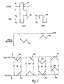
- the strobe pulse voltage waveform 10 is a unidirectional pulse of height V s and duration t.
- An ON data pulse voltage waveform 11 a is a balanced bipolar pulse making an excursion to -V D for a time t and then an excursion to +V D for a further time t.
- An OFF data pulse waveform 11 b is the inverse of the ON data pulse waveform.
- Any given pixel which is defined by the area of intersection of a particular row electrode with a particular column electrode, will receive a succession of data pulses that address other pixels in the same column.
- the first half of an ON data pulse will tend to drive that pixel a little way towards the ON state, and then the second half will tend to drive it the same amount in the reverse direction and thus restore the status quo.
- This effect is depicted at 12a.
- the effect of an OFF data pulse is first to tend to drive the pixel towards the OFF state, and then to restore the original state as depicted at 12b.
- the effect of ON data pulses is to drive the pixel a little way towards the ON state, and then restore the saturated OFF state, as depicted at 14a.
- the first OFF data pulse introduces a difference because the first half of such a pulse cannot drive the saturated OFF pixel any further OFF.
- the result is that at the end of the first OFF pulse a pixel previously in a fully saturated OFF state is driven a small amount ON, as depicted at 14b. Thereafter that pixel will make further temporary excursions either back to the fully OFF state, as depicted at 15b, or to a state that is slightly further ON, as depicted at 15a.
- there is no staircase effect because both types of data pulse end up by restoring the state that existed before commencement of the data pulse.
- the fully ON state is depicted at 16, and it is seen that here there is an analogous situation, with the first ON data pulse driving the pixel a small amount OFF, as depicted at 17a. With any data pulse after the first ON data pulse, the pixel always comes to rest at this level at the end of the data pulse irrespective of whether the data pulse is an ON or an OFF pulse, as depicted at 18a and 18b.
- the strobe pulse coincides with the first half of the data pulse, and hence the combined effect in the first half of the data pulse is the application of a voltage of (Vg+V o ) tending to turn the pixel ON. Then, in the second half of the data pulse, there is a voltage V D tending to turn the pixel OFF.
- Vg+V o a voltage of (Vg+V o )
- V D a voltage
- This first addressing scheme uses a unidirectional strobing pulse for data entry, and so it does not of itself permit the use of the data pulses to set some pixels into the ON state while at the same time setting others into the OFF state. Therefore, it is necessary to blank the cell before addressing.
- This can be done on a line-by-line basis by inserting a blanking pulse of opposite polarity to the strobing pulse on to the row electrode in the time interval terminating with the commencement of data entry for that row, and starting with the commencement of the data entry for the preceding line.
- blanking can be effected on a page basis by applying blanking pulses simultaneously to all the rows before starting a frame.
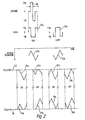
- the addressing scheme of Figure 2 uses a balanced bipolar strobing pulse waveform, and thus with this scheme it is possible for data to be entered and to be erased without recourse to page or line blanking techniques.
- the first half of the Figure 2 scheme strobe pules 20 consists of a pulse of height V s and duration t. This is immediately followed by a pulse of height -V s and duration t.
- An ON data pulse voltage waveform 21a a is also a balanced bipolar pulse, and makes an excursion +V D for a time t, then an excursion to -V D for a time 2t, and finally an excursion to +V D again for a further time t.
- An OFF data pulse waveform 21b is the inverse of the ON data pulse waveform.
- the fully ON state is depicted at 26, and it is seen that here there is an analogous situation insofar as both type of data pulse, occurring in the absence of a strobing pulse, leave a fully ON pixel driven a small way towards the OFF state as depicted by waveforms 27a and 27b.
- waveforms 27a and 27b depicted by waveforms 27a and 27b.
- the strobing pulse is synchronised with the second and third quarters of data pulses.
- the pixel in the case of a strobe pulse synchronised with an ON pulse waveform, the pixel is exposed to a voltage (V s +V D ) in the second quarter of the data pulse waveform, which is in a direction driving the pixel into the fully ON state.
- the pixel In the third quarter, the pixel is exposed to a voltage (V s -V D ) tending to turn it OFF, and in the fourth quarter it is exposed to a voltage V D also tending to turn it OFF.
- V s +V D a voltage
- V D voltage
- the addressing scheme of Figure 3 uses the same form of balanced bipolar strobing pulse 30 as is employed in the scheme of Figure 2, but in this instance it is synchronised with the third and fourth quarters of the data pulse waveforms instead of the second and third quarters. This change necessitates changes to the data pulse waveforms.
- An ON data pulse waveform 31 still retains a balanced bipolar format, and makes an excursion +V D for a time 2t for the first half of the waveform duration, and then an excursion to -V D for 2t to complete the waveform.
- the OFF data pulse waveform 31b b is, as before, the inverse of the ON data pulse waveform.
- each of the three examples has used a strobing pulse length that is exactly half the length of a data pulse, but it will be evident that at least in principle it would be possible to extend the data pulses, whilst preserving their balanced format, and thus make the duration longer than twice that of a strobing pulse. Such a procedure would have the disadvantage of slowing the speed, and hence is not generally to be desired.
Description
- This invention relates to the addressing of matrix array type ferro-electric liquid crystal display devices.
- Hitherto dynamic scattering mode liquid crystal display devices have been operated using a d.c. drive or an a.c. one, whereas field effect mode liquid crystal devices have generally been operated using an a.c. drive in order to avoid performance impairment problems associated with electrolytic degradation of the liquid crystal layer. Such devices have employed liquid crystals that do not exhibit ferro-electricity, and the material interacts with an applied electric field by way of an induced dipole. As a result they are not sensitive to the polarity of the applied field, but respond to the applied RMS voltage averaged over approximately one response time at that voltage. There may also be frequency dependence as in the case of so-called two-frequency materials, but this only affects the type of response produced by the applied field.
- In contrast to this a ferro-electric liquid crystal exhibits a permanent electric dipole, and it is this permanent dipole which will interact with an applied electric field. Ferro-electric liquid crystals are of interest in display applications because they are expected to show a greater coupling with an applied field than that typical of a liquid crystal that relies on coupling with an induced dipole, and hence ferro-electric liquid crystals are expected to show a faster response. A ferro- electric liquid crystal display mode is described for instance by N. A. Clark et al in a paper entitled 'Ferro-electric Liquid Crystal Electro-Optics Using the Surface Stabilized Structure' appearing in Mol. Cryst. Liq. Cryst. 1983 Volume 94 pages 213 to 234. Two properties of ferro-electrics set the problems of matrix addressing such devices apart from the addressing of non-ferro-electric devices. First they are polarity sensitive, and second their response times exhibit a relatively weak dependence upon applied voltage. The response time of a ferro-electric is typically proportional to the inverse square of applied voltage, or even worse, proportional to the inverse single power of voltage; whereas a non-ferro-electric smectic A, which in certain other respects is a comparable device exhibiting long term storage capability, exhibits a response time that is typically proportional to the inverse fifth power of voltage.
- Therefore, a good drive scheme for addressing a ferro-electric liquid crystal display must keep to a minimum the incidence of wrong polarity signals to any given pixel, whether it is intended as an ON pixel or an OFF pixel.
- With reference to French patent application FR-A-2 544 844A published 26th October 1984, the applicant has voluntarily limited the scope of the present application, and submitted separate claims 1A-4A for France.
- According to the present invention there is provided a method of addressing a matrix array type liquid crystal display device with a ferro- electric liquid crystal layer whose pixels are defined by the areas of overlap between the members of a first set of electrodes on one side of the liquid crystal layer and the members of a second set of electrodes on the other side of the layer, characterised in that strobing pulses are applied serially to the members of the first set while data pulses are applied in parallel to the second set in order to address the cell line by line, and wherein the waveform of a data pulse is balanced bipolar and twice the duration of a strobing pulse.
- There follows a description of the manner of addressing ferro-electric liquid crystal matrix array devices by methods embodying the invention in preferred forms. The description refers to the accompanying drawings in which Figures 1 to 3 depict waveforms associated with three alternative addressing schemes.
- All three addressing schemes now to be described involve addressing the display on a line by line basis using a parallel input of data pulses on a set of column electrodes while a strobing pulse is applied to each of the row electrodes in turn.
- In the scheme of Figure 1 the strobe
pulse voltage waveform 10 is a unidirectional pulse of height Vs and duration t. An ON datapulse voltage waveform 11 a is a balanced bipolar pulse making an excursion to -VD for a time t and then an excursion to +VD for a further time t. An OFFdata pulse waveform 11 b is the inverse of the ON data pulse waveform. - Any given pixel, which is defined by the area of intersection of a particular row electrode with a particular column electrode, will receive a succession of data pulses that address other pixels in the same column. When some other row is being strobed, the first half of an ON data pulse will tend to drive that pixel a little way towards the ON state, and then the second half will tend to drive it the same amount in the reverse direction and thus restore the status quo. This effect is depicted at 12a. Similarly the effect of an OFF data pulse is first to tend to drive the pixel towards the OFF state, and then to restore the original state as depicted at 12b.
- If the pixel is in a fully OFF state as depicted by the
line 13, the effect of ON data pulses is to drive the pixel a little way towards the ON state, and then restore the saturated OFF state, as depicted at 14a. The first OFF data pulse introduces a difference because the first half of such a pulse cannot drive the saturated OFF pixel any further OFF. The result is that at the end of the first OFF pulse a pixel previously in a fully saturated OFF state is driven a small amount ON, as depicted at 14b. Thereafter that pixel will make further temporary excursions either back to the fully OFF state, as depicted at 15b, or to a state that is slightly further ON, as depicted at 15a. However, it is to be particularly noted that there is no staircase effect because both types of data pulse end up by restoring the state that existed before commencement of the data pulse. - The fully ON state is depicted at 16, and it is seen that here there is an analogous situation, with the first ON data pulse driving the pixel a small amount OFF, as depicted at 17a. With any data pulse after the first ON data pulse, the pixel always comes to rest at this level at the end of the data pulse irrespective of whether the data pulse is an ON or an OFF pulse, as depicted at 18a and 18b.
- Thus far consideration has been confined to the operation of the pixel while the strobing pulse is addressing other rows.
- Considering first the effect of a strobe pulse coinciding with an ON data pulse, the strobe pulse coincides with the first half of the data pulse, and hence the combined effect in the first half of the data pulse is the application of a voltage of (Vg+Vo) tending to turn the pixel ON. Then, in the second half of the data pulse, there is a voltage VD tending to turn the pixel OFF. In order for the pixel to be switched on by this sequence of events it is clearly necessary for the ON voltage duration, t, divided by the response time at that voltage, T(Vs+VD), to be greater than unity.

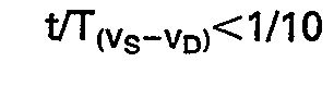
- Considering now the effect of a strobe pulse coinciding with an OFF data pulse. The combined effect in the first half of the data pulse is the application of a voltage (VS-VD) tending to turn the pixel ON. This is then followed in the second half by a further voltage VD also tending to turn the pixel ON. Clearly the 'worst' case is when the pixel is not starting from the fully OFF state, but has already been turned partly ON by a preceding OFF data pulse. Under these conditions an OFF element has to withstand two pulses of duration t and voltage Vo, and a single pulse of duration t and voltage VS-VD without switching on to any appreciable extent. This can be expressed by the relationship
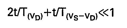
- For a typical response characteristic this is satisfied by

- Inspection of Figure 1 reveals that if the strobing pulse is synchronised with the second halves of the data pulses instead of with their first halves, substantially the same situation prevails, though the roles of the data pulse waveforms are interchanged.
- This first addressing scheme uses a unidirectional strobing pulse for data entry, and so it does not of itself permit the use of the data pulses to set some pixels into the ON state while at the same time setting others into the OFF state. Therefore, it is necessary to blank the cell before addressing. This can be done on a line-by-line basis by inserting a blanking pulse of opposite polarity to the strobing pulse on to the row electrode in the time interval terminating with the commencement of data entry for that row, and starting with the commencement of the data entry for the preceding line. Alternatively blanking can be effected on a page basis by applying blanking pulses simultaneously to all the rows before starting a frame.
- The addressing scheme of Figure 2 uses a balanced bipolar strobing pulse waveform, and thus with this scheme it is possible for data to be entered and to be erased without recourse to page or line blanking techniques.
- The first half of the Figure 2
scheme strobe pules 20 consists of a pulse of height Vs and duration t. This is immediately followed by a pulse of height -Vs and duration t. An ON datapulse voltage waveform 21a a is also a balanced bipolar pulse, and makes an excursion +VD for a time t, then an excursion to -VD for a time 2t, and finally an excursion to +VD again for a further time t. An OFFdata pulse waveform 21b is the inverse of the ON data pulse waveform. - The effects of ON and OFF data pulse waveforms in the absence of any strobing pulses are depicted respectively at 22a and 22b. In this instance both types of data pulse have the effect, on their own, of leaving a pixel previously in a fully
OFF state 23 in a state driven a small amount ON as depicted by waveforms 24a. and 24b. Thereafter anyfurther data pulse - The fully ON state is depicted at 26, and it is seen that here there is an analogous situation insofar as both type of data pulse, occurring in the absence of a strobing pulse, leave a fully ON pixel driven a small way towards the OFF state as depicted by
waveforms - The strobing pulse is synchronised with the second and third quarters of data pulses. Thus, in the case of a strobe pulse synchronised with an ON pulse waveform, the pixel is exposed to a voltage (Vs+VD) in the second quarter of the data pulse waveform, which is in a direction driving the pixel into the fully ON state. In the third quarter, the pixel is exposed to a voltage (Vs-VD) tending to turn it OFF, and in the fourth quarter it is exposed to a voltage VD also tending to turn it OFF. The complementary situation occurs in the case of a strobing pulse synchronised with an OFF data pulse waveform.
- The requirement that the pixel be driven to saturation in the duration t of the second quarter of the data pulse waveform is once again given by the expression

- Since the third and fourth quarters of the data pulse waveform co-operate in tending to drive the pixel away from saturation, it is necessary to ensure that their combined effect is small enough not to remove the pixel from its saturated state to too significant an extent. This can be expressed by the relationship


- The addressing scheme of Figure 3 uses the same form of balanced
bipolar strobing pulse 30 as is employed in the scheme of Figure 2, but in this instance it is synchronised with the third and fourth quarters of the data pulse waveforms instead of the second and third quarters. This change necessitates changes to the data pulse waveforms. An ON data pulse waveform 31 still retains a balanced bipolar format, and makes an excursion +VD for a time 2t for the first half of the waveform duration, and then an excursion to -VD for 2t to complete the waveform. The OFFdata pulse waveform 31b b is, as before, the inverse of the ON data pulse waveform. - The effects of ON and OFF data pulse waveforms in the absence of any strobing pulses are depicted respectively at 32a and 32b. As depicted by
waveform 34b, an OFF data pulse waveform on its own has the effect of leaving in a fully OFF state a pixel that was previously in the fully OFF state 33. Similarly as depicted by waveform 37a, an ON data pulse waveform on its own has the effect of leaving in a fully ON state a pixel that was previously in the fully ON state 36. In contrast to this ON or OFF data pulse waveforms that are applied on their own to pixels that are respectively in their fully OFF and fully ON states have the effect of leaving those pixels in states that are driven slightly away from saturation, as depicted respectively bywaveforms 34a and 37b, by a voltage excursion of VD maintained for a duration 2t. - The use of balanced bipolar data pulse waveforms again ensures that a succession of data pulses is incapable of producing a staircase effect. Once the condition is reached that a data pulse waveform does not attempt to drive a pixel beyond saturation, further data pulses, occurring in the absence of strobing pulses, will each leave a pixel in the state it was in before the start of that pulse.
- Inspection of the three
waveforms -


- Making the same assumption as before, these last two relationships can be expressed as

- A similar situation pertains if the strobe pulse is synchronised with the first and second quarters of the data pulses instead of with their third and fourth quarters, but in this instance the roles of the data pulses are reversed.
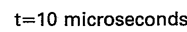
- The absolute magnitudes of Vs, VD and twill depend upon the characteristics of the particular display device concerned. In some cases the choice can be quite critical unless the 'one tenth' criterion is relaxed. Thus for instance, with the characteristics quoted by N. A. Clark and S. T. Lagerwall in "Recent Developments in Condensed Matter Physics", Volume 4 (1981) pp 309 to 319, without relaxing this criterion it has not been found possible to use the scheme of Figure 1 at all, while the scheme of Figure 2 will just function for an address time t of 15 microseconds with Vs=2.70 volts and VD=1.37 volts, but will not function if the address time t is reduced to 10 microseconds or expanded to 20 microseconds. (In this context it is to be noted that for the schemes of Figures 2 and 3 the line time is equal to 4t.) However, the scheme of Figure 3 is easier to operate under these conditions and will operate for example with


- In the foregoing specific description each of the three examples has used a strobing pulse length that is exactly half the length of a data pulse, but it will be evident that at least in principle it would be possible to extend the data pulses, whilst preserving their balanced format, and thus make the duration longer than twice that of a strobing pulse. Such a procedure would have the disadvantage of slowing the speed, and hence is not generally to be desired.
Claims (8)
Applications Claiming Priority (2)
| Application Number | Priority Date | Filing Date | Title |
|---|---|---|---|
| GB8324304 | 1983-09-10 | ||
| GB08324304A GB2146473B (en) | 1983-09-10 | 1983-09-10 | Addressing liquid crystal displays |
Publications (3)
| Publication Number | Publication Date |
|---|---|
| EP0137726A2 EP0137726A2 (en) | 1985-04-17 |
| EP0137726A3 EP0137726A3 (en) | 1987-09-02 |
| EP0137726B1 true EP0137726B1 (en) | 1990-10-03 |
Family
ID=10548623
Family Applications (1)
| Application Number | Title | Priority Date | Filing Date |
|---|---|---|---|
| EP84306127A Expired EP0137726B1 (en) | 1983-09-10 | 1984-09-07 | Addressing liquid crystal displays |
Country Status (5)
| Country | Link |
|---|---|
| US (1) | US4638310A (en) |
| EP (1) | EP0137726B1 (en) |
| JP (1) | JPS60173591A (en) |
| AU (1) | AU3285584A (en) |
| GB (1) | GB2146473B (en) |
Families Citing this family (67)
| Publication number | Priority date | Publication date | Assignee | Title |
|---|---|---|---|---|
| US4655561A (en) * | 1983-04-19 | 1987-04-07 | Canon Kabushiki Kaisha | Method of driving optical modulation device using ferroelectric liquid crystal |
| US5093737A (en) * | 1984-02-17 | 1992-03-03 | Canon Kabushiki Kaisha | Method for driving a ferroelectric optical modulation device therefor to apply an erasing voltage in the first step |
| GB2149176B (en) * | 1983-10-26 | 1988-07-13 | Stc Plc | Addressing liquid crystal displays |
| GB2149554B (en) * | 1983-11-08 | 1987-04-01 | Standard Telephones Cables Ltd | Data terminals |
| JPS6194026A (en) * | 1984-10-15 | 1986-05-12 | Seiko Instr & Electronics Ltd | Smectic liquid crystal display device |
| DE3501982A1 (en) * | 1984-01-23 | 1985-07-25 | Canon K.K., Tokio/Tokyo | METHOD FOR DRIVING A LIGHT MODULATION DEVICE |
| US5296953A (en) * | 1984-01-23 | 1994-03-22 | Canon Kabushiki Kaisha | Driving method for ferro-electric liquid crystal optical modulation device |
| US5633652A (en) * | 1984-02-17 | 1997-05-27 | Canon Kabushiki Kaisha | Method for driving optical modulation device |
| JPS6150119A (en) * | 1984-08-20 | 1986-03-12 | Hitachi Ltd | Driving circuit for liquid crystal display device |
| JPS6194027A (en) * | 1984-10-15 | 1986-05-12 | Seiko Instr & Electronics Ltd | Smectic liquid crystal display device |
| ATE74674T1 (en) * | 1984-11-14 | 1992-04-15 | Northern Telecom Ltd | TWO-DIMENSIONAL OPTICAL INFORMATION PROCESSING DEVICE. |
| GB2173337B (en) * | 1985-04-03 | 1989-01-11 | Stc Plc | Addressing liquid crystal cells |
| GB2173336B (en) * | 1985-04-03 | 1988-04-27 | Stc Plc | Addressing liquid crystal cells |
| GB2173335B (en) * | 1985-04-03 | 1988-02-17 | Stc Plc | Addressing liquid crystal cells |
| GB2175725B (en) * | 1985-04-04 | 1989-10-25 | Seikosha Kk | Improvements in or relating to electro-optical display devices |
| US4778260A (en) * | 1985-04-22 | 1988-10-18 | Canon Kabushiki Kaisha | Method and apparatus for driving optical modulation device |
| US4844590A (en) * | 1985-05-25 | 1989-07-04 | Canon Kabushiki Kaisha | Method and apparatus for driving ferroelectric liquid crystal device |
| JPH0750268B2 (en) * | 1985-07-08 | 1995-05-31 | セイコーエプソン株式会社 | Liquid crystal element driving method |
| GB2178582B (en) * | 1985-07-16 | 1990-01-24 | Canon Kk | Liquid crystal apparatus |
| JPH0758371B2 (en) * | 1985-07-31 | 1995-06-21 | セイコーエプソン株式会社 | Liquid crystal element driving method |
| FR2590392B1 (en) * | 1985-09-04 | 1994-07-01 | Canon Kk | FERROELECTRIC LIQUID CRYSTAL DEVICE |
| US5011269A (en) * | 1985-09-06 | 1991-04-30 | Matsushita Electric Industrial Co., Ltd. | Method of driving a ferroelectric liquid crystal matrix panel |
| JPS6256935A (en) * | 1985-09-06 | 1987-03-12 | Matsushita Electric Ind Co Ltd | Driving method for liquid crystal matrix panel |
| JPS62112128A (en) * | 1985-11-11 | 1987-05-23 | Semiconductor Energy Lab Co Ltd | Liquid crystal device |
| US4836656A (en) * | 1985-12-25 | 1989-06-06 | Canon Kabushiki Kaisha | Driving method for optical modulation device |
| JPS62150334A (en) * | 1985-12-25 | 1987-07-04 | Canon Inc | Driving method for optical modulation element |
| US5255110A (en) * | 1985-12-25 | 1993-10-19 | Canon Kabushiki Kaisha | Driving method for optical modulation device using ferroelectric liquid crystal |
| JPS62204233A (en) * | 1986-03-05 | 1987-09-08 | Hitachi Ltd | Liquid crystal matrix driving device |
| JPS62161129A (en) * | 1986-01-10 | 1987-07-17 | Hitachi Ltd | Liquid matrix driving method |
| ES2064306T3 (en) * | 1986-02-21 | 1995-02-01 | Canon Kk | DISPLAY DEVICE. |
| JPS62218943A (en) * | 1986-03-19 | 1987-09-26 | Sharp Corp | Liquid crystal display device |
| GB2173629B (en) * | 1986-04-01 | 1989-11-15 | Stc Plc | Addressing liquid crystal cells |
| JPS62280825A (en) * | 1986-05-30 | 1987-12-05 | Nec Corp | Driving method for liquid crystal element |
| NL8601804A (en) * | 1986-07-10 | 1988-02-01 | Philips Nv | METHOD FOR CONTROLLING A DISPLAY DEVICE AND A DISPLAY DEVICE SUITABLE FOR SUCH A METHOD |
| EP0256548B1 (en) * | 1986-08-18 | 1993-03-17 | Canon Kabushiki Kaisha | Method and apparatus for driving optical modulation device |
| JPS6373228A (en) * | 1986-09-17 | 1988-04-02 | Canon Inc | Method for driving optical modulating element |
| JPS63116128A (en) * | 1986-11-04 | 1988-05-20 | Canon Inc | Driving method for optical modulating element |
| JPS63137214A (en) * | 1986-11-29 | 1988-06-09 | Toppan Printing Co Ltd | Matrix driving method for liquid crystal display device |
| JPS63198097A (en) * | 1987-02-13 | 1988-08-16 | セイコーインスツルメンツ株式会社 | Non-linear 2-terminal type active matrix display device |
| US5182549A (en) * | 1987-03-05 | 1993-01-26 | Canon Kabushiki Kaisha | Liquid crystal apparatus |
| SE466423B (en) * | 1987-06-01 | 1992-02-10 | Gen Electric | SET AND DEVICE FOR ELIMINATION OF OVERHEALING IN MATRIX ADDRESSED THINFILM TRANSISTOR IMAGE UNITS WITH LIQUID CRYSTALS |
| US4873516A (en) * | 1987-06-01 | 1989-10-10 | General Electric Company | Method and system for eliminating cross-talk in thin film transistor matrix addressed liquid crystal displays |
| US5010328A (en) * | 1987-07-21 | 1991-04-23 | Thorn Emi Plc | Display device |
| US5642128A (en) * | 1987-10-02 | 1997-06-24 | Canon Kabushiki Kaisha | Display control device |
| US4870398A (en) * | 1987-10-08 | 1989-09-26 | Tektronix, Inc. | Drive waveform for ferroelectric displays |
| US4857906A (en) * | 1987-10-08 | 1989-08-15 | Tektronix, Inc. | Complex waveform multiplexer for liquid crystal displays |
| US4915477A (en) * | 1987-10-12 | 1990-04-10 | Seiko Epson Corporation | Method for driving an electro-optical device wherein erasing data stored in each pixel by providing each scan line and data line with an erasing signal |
| GB8728433D0 (en) * | 1987-12-04 | 1988-01-13 | Emi Plc Thorn | Display device |
| NL8703040A (en) * | 1987-12-16 | 1989-07-17 | Philips Nv | METHOD FOR CONTROLLING A PASSIVE FERRO-ELECTRIC LIQUID CRYSTAL DISPLAY. |
| NL8703085A (en) * | 1987-12-21 | 1989-07-17 | Philips Nv | METHOD FOR CONTROLLING A DISPLAY DEVICE |
| JPS6426823A (en) * | 1988-04-28 | 1989-01-30 | Seiko Instr & Electronics | Ferroelectric liquid crystal electro-optic device |
| US4839384A (en) * | 1988-10-07 | 1989-06-13 | E. R. Squibb & Sons, Inc. | Method of inhibiting onset of or treating migraine headache using a thromboxane A2 receptor antagonist |
| GB2225473B (en) * | 1988-11-23 | 1993-01-13 | Stc Plc | Addressing scheme for multiplexded ferroelectric liquid crystal |
| US5289175A (en) * | 1989-04-03 | 1994-02-22 | Canon Kabushiki Kaisha | Method of and apparatus for driving ferroelectric liquid crystal display device |
| US5815130A (en) * | 1989-04-24 | 1998-09-29 | Canon Kabushiki Kaisha | Chiral smectic liquid crystal display and method of selectively driving the scanning and data electrodes |
| US5034736A (en) * | 1989-08-14 | 1991-07-23 | Polaroid Corporation | Bistable display with permuted excitation |
| JP2584871B2 (en) * | 1989-08-31 | 1997-02-26 | キヤノン株式会社 | Display device |
| US5095377A (en) * | 1990-08-02 | 1992-03-10 | Matsushita Electric Industrial Co., Ltd. | Method of driving a ferroelectric liquid crystal matrix panel |
| US5963186A (en) * | 1990-08-07 | 1999-10-05 | The Secretary Of State For Defence In Her Britannic Majesty's Government Of The United Kingdom Of Great Britain And Northern Ireland | Multiplex addressing of ferro-electric liquid crystal displays |
| JPH05224625A (en) * | 1992-02-12 | 1993-09-03 | Nec Corp | Driving method for liquid crystal display device |
| JP3307486B2 (en) * | 1993-11-19 | 2002-07-24 | 富士通株式会社 | Flat panel display and control method thereof |
| KR100383337B1 (en) * | 1994-06-23 | 2003-07-22 | 코닌클리케 필립스 일렉트로닉스 엔.브이. | Display Units and Color Projection Systems |
| US5767829A (en) * | 1994-08-23 | 1998-06-16 | U.S. Philips Corporation | Liquid crystal display device including drive circuit for predetermining polarization state |
| JPH09127483A (en) * | 1995-11-06 | 1997-05-16 | Sharp Corp | Liquid crystal display device |
| GB9612958D0 (en) * | 1996-06-20 | 1996-08-21 | Sharp Kk | Matrix array bistable device addressing |
| US5937906A (en) * | 1997-05-06 | 1999-08-17 | Kozyuk; Oleg V. | Method and apparatus for conducting sonochemical reactions and processes using hydrodynamic cavitation |
| DK1991566T3 (en) | 2006-02-28 | 2015-04-27 | Suntory Holdings Ltd | A gene encoding a protein responsible for flocculation of yeast, and its use |
Family Cites Families (21)
| Publication number | Priority date | Publication date | Assignee | Title |
|---|---|---|---|---|
| CH529421A (en) * | 1971-03-30 | 1972-10-15 | Bbc Brown Boveri & Cie | Circuit arrangement for controlling liquid-crystalline light valves which can be addressed in matrix form |
| JPS523560B1 (en) * | 1971-06-02 | 1977-01-28 | ||
| JPS5114434B1 (en) * | 1971-07-29 | 1976-05-10 | ||
| JPS5715393B2 (en) * | 1973-04-20 | 1982-03-30 | ||
| US3911421A (en) * | 1973-12-28 | 1975-10-07 | Ibm | Selection system for matrix displays requiring AC drive waveforms |
| JPS5416894B2 (en) * | 1974-03-01 | 1979-06-26 | ||
| US4040720A (en) * | 1975-04-21 | 1977-08-09 | Rockwell International Corporation | Ferroelectric liquid crystal display |
| US4100540A (en) * | 1975-11-18 | 1978-07-11 | Citizen Watch Co., Ltd. | Method of driving liquid crystal matrix display device to obtain maximum contrast and reduce power consumption |
| JPS52103993A (en) * | 1976-02-11 | 1977-08-31 | Rank Organisation Ltd | Liquid crystal display unit |
| US4060801A (en) * | 1976-08-13 | 1977-11-29 | General Electric Company | Method and apparatus for non-scan matrix addressing of bar displays |
| JPS5335432A (en) * | 1976-09-14 | 1978-04-01 | Canon Inc | Display unit |
| GB1565364A (en) * | 1976-10-29 | 1980-04-16 | Smiths Industries Ltd | Display apparatus |
| US4180813A (en) * | 1977-07-26 | 1979-12-25 | Hitachi, Ltd. | Liquid crystal display device using signal converter of digital type |
| JPS5483694A (en) * | 1977-12-16 | 1979-07-03 | Hitachi Ltd | Nematic liquid crystal body for display device |
| US4443062A (en) * | 1979-09-18 | 1984-04-17 | Citizen Watch Company Limited | Multi-layer display device with nonactive display element groups |
| NL8003930A (en) * | 1980-07-08 | 1982-02-01 | Philips Nv | DISPLAY WITH A LIQUID CRYSTAL. |
| US4404555A (en) * | 1981-06-09 | 1983-09-13 | Northern Telecom Limited | Addressing scheme for switch controlled liquid crystal displays |
| US4427978A (en) * | 1981-08-31 | 1984-01-24 | Marshall Williams | Multiplexed liquid crystal display having a gray scale image |
| GB2118346B (en) * | 1982-04-01 | 1985-07-24 | Standard Telephones Cables Ltd | Scanning liquid crystal display cells |
| JPS58173718A (en) * | 1982-04-07 | 1983-10-12 | Hitachi Ltd | Optical modulating device of liquid crystal and its production |
| US4571585A (en) * | 1983-03-17 | 1986-02-18 | General Electric Company | Matrix addressing of cholesteric liquid crystal display |
-
1983
- 1983-09-10 GB GB08324304A patent/GB2146473B/en not_active Expired
-
1984
- 1984-09-06 US US06/647,567 patent/US4638310A/en not_active Expired - Fee Related
- 1984-09-07 EP EP84306127A patent/EP0137726B1/en not_active Expired
- 1984-09-10 JP JP59188253A patent/JPS60173591A/en active Granted
- 1984-09-10 AU AU32855/84A patent/AU3285584A/en not_active Abandoned
Also Published As
| Publication number | Publication date |
|---|---|
| EP0137726A3 (en) | 1987-09-02 |
| AU3285584A (en) | 1985-03-14 |
| GB2146473A (en) | 1985-04-17 |
| US4638310A (en) | 1987-01-20 |
| GB2146473B (en) | 1987-03-11 |
| EP0137726A2 (en) | 1985-04-17 |
| JPS60173591A (en) | 1985-09-06 |
| GB8324304D0 (en) | 1983-10-12 |
| JPH0344284B2 (en) | 1991-07-05 |
Similar Documents
| Publication | Publication Date | Title |
|---|---|---|
| EP0137726B1 (en) | Addressing liquid crystal displays | |
| EP0197742B1 (en) | Addressing liquid crystal cells | |
| US4909607A (en) | Addressing liquid crystal cells | |
| CA2049624C (en) | Liquid crystal apparatus | |
| US4728947A (en) | Addressing liquid crystal cells using bipolar data strobe pulses | |
| JP2810692B2 (en) | Display device using ferroelectric liquid crystal and addressing method for the display device | |
| GB2180385A (en) | Driving display devices | |
| GB2218842A (en) | Liquid crystal cell addressing | |
| JP3638288B2 (en) | Liquid crystal display | |
| JPS6033535A (en) | Driving method of optical modulating element | |
| US5006839A (en) | Method for driving a liquid crystal optical apparatus | |
| EP0196905A2 (en) | Addressing liquid crystal cells | |
| JPH0437412B2 (en) | ||
| JP2572578B2 (en) | Image display device and driving method thereof | |
| JP2727131B2 (en) | Driving method of active matrix liquid crystal device | |
| EP0247806A2 (en) | Method for driving a ferroelectric liquid crystal electro-optical device | |
| JP2615690B2 (en) | Driving method of optical modulation element | |
| JP2718063B2 (en) | Driving method of liquid crystal device | |
| KR920007127B1 (en) | Method for driving a liquid crystal optical apparatus | |
| JPH08137438A (en) | Method for driving optical modulation element | |
| JPH0749480A (en) | Method for driving matrix of flat type display device | |
| JPH06148599A (en) | Driving method for liquid crystal display device | |
| JPS63151929A (en) | Driving method for optical modulating element | |
| JPH0660978B2 (en) | Optical modulator | |
| JPH03271715A (en) | Driving method for active matrix liquid crystal element |
Legal Events
| Date | Code | Title | Description |
|---|---|---|---|
| PUAI | Public reference made under article 153(3) epc to a published international application that has entered the european phase |
Free format text: ORIGINAL CODE: 0009012 |
|
| AK | Designated contracting states |
Designated state(s): BE CH FR LI LU NL SE |
|
| PUAL | Search report despatched |
Free format text: ORIGINAL CODE: 0009013 |
|
| AK | Designated contracting states |
Kind code of ref document: A3 Designated state(s): BE CH FR LI LU NL SE |
|
| 17P | Request for examination filed |
Effective date: 19870805 |
|
| 17Q | First examination report despatched |
Effective date: 19890607 |
|
| RAP1 | Party data changed (applicant data changed or rights of an application transferred) |
Owner name: STC PLC |
|
| GRAA | (expected) grant |
Free format text: ORIGINAL CODE: 0009210 |
|
| AK | Designated contracting states |
Kind code of ref document: B1 Designated state(s): BE CH FR LI LU NL SE |
|
| ET | Fr: translation filed | ||
| PLBE | No opposition filed within time limit |
Free format text: ORIGINAL CODE: 0009261 |
|
| STAA | Information on the status of an ep patent application or granted ep patent |
Free format text: STATUS: NO OPPOSITION FILED WITHIN TIME LIMIT |
|
| 26N | No opposition filed | ||
| PG25 | Lapsed in a contracting state [announced via postgrant information from national office to epo] |
Ref country code: LU Free format text: LAPSE BECAUSE OF NON-PAYMENT OF DUE FEES Effective date: 19910930 |
|
| BECH | Be: change of holder |
Free format text: 931231 *NORTHERN TELECOM LTD |
|
| BECN | Be: change of holder's name |
Effective date: 19931231 |
|
| REG | Reference to a national code |
Ref country code: CH Ref legal event code: PUE Owner name: NORTHERN TELECOM LIMITED |
|
| NLT1 | Nl: modifications of names registered in virtue of documents presented to the patent office pursuant to art. 16 a, paragraph 1 |
Owner name: STC LIMITED TE LONDEN, GROOT-BRITTANNIE. |
|
| NLT1 | Nl: modifications of names registered in virtue of documents presented to the patent office pursuant to art. 16 a, paragraph 1 |
Owner name: NORTHERN TELECOM EUROPE LIMITED TE LONDON, GROOT-B |
|
| NLT1 | Nl: modifications of names registered in virtue of documents presented to the patent office pursuant to art. 16 a, paragraph 1 |
Owner name: STC LIMITED TE MAIDENHEAD, GROOT-BRITTANNIE. |
|
| NLS | Nl: assignments of ep-patents |
Owner name: NORTHERN TELECOM LIMITED IN MONTREAL, CANADA |
|
| EAL | Se: european patent in force in sweden |
Ref document number: 84306127.6 |
|
| REG | Reference to a national code |
Ref country code: CH Ref legal event code: PFA Free format text: NORTEL NETWORKS CORPORATION TRANSFER- NORTEL NETWORKS LIMITED * NORTHERN TELECOM LIMITED TRANSFER- NORTEL NETWORKS CORPORATION Ref country code: CH Ref legal event code: NV Representative=s name: CRONIN INTELLECTUAL PROPERTY |
|
| NLT1 | Nl: modifications of names registered in virtue of documents presented to the patent office pursuant to art. 16 a, paragraph 1 |
Owner name: NORTEL NETWORKS LIMITED;NORTHERN TELECOM LIMITED |
|
| BECN | Be: change of holder's name |
Effective date: 20020307 |
|
| PGFP | Annual fee paid to national office [announced via postgrant information from national office to epo] |
Ref country code: CH Payment date: 20030826 Year of fee payment: 20 |
|
| PGFP | Annual fee paid to national office [announced via postgrant information from national office to epo] |
Ref country code: NL Payment date: 20030828 Year of fee payment: 20 |
|
| PGFP | Annual fee paid to national office [announced via postgrant information from national office to epo] |
Ref country code: FR Payment date: 20030902 Year of fee payment: 20 |
|
| PGFP | Annual fee paid to national office [announced via postgrant information from national office to epo] |
Ref country code: SE Payment date: 20030903 Year of fee payment: 20 |
|
| PGFP | Annual fee paid to national office [announced via postgrant information from national office to epo] |
Ref country code: BE Payment date: 20031009 Year of fee payment: 20 |
|
| PG25 | Lapsed in a contracting state [announced via postgrant information from national office to epo] |
Ref country code: LI Free format text: LAPSE BECAUSE OF EXPIRATION OF PROTECTION Effective date: 20040906 Ref country code: CH Free format text: LAPSE BECAUSE OF EXPIRATION OF PROTECTION Effective date: 20040906 |
|
| PG25 | Lapsed in a contracting state [announced via postgrant information from national office to epo] |
Ref country code: NL Free format text: LAPSE BECAUSE OF EXPIRATION OF PROTECTION Effective date: 20040907 |
|
| BE20 | Be: patent expired |
Owner name: *NORTEL NETWORKS LTD Effective date: 20040907 |
|
| REG | Reference to a national code |
Ref country code: CH Ref legal event code: PL |
|
| NLV7 | Nl: ceased due to reaching the maximum lifetime of a patent |
Effective date: 20040907 |
|
| EUG | Se: european patent has lapsed | ||
| REG | Reference to a national code |
Ref country code: SE Ref legal event code: EUG |