EP0136111A2 - Real time seismic telemetry system - Google Patents
Real time seismic telemetry system Download PDFInfo
- Publication number
- EP0136111A2 EP0136111A2 EP84305935A EP84305935A EP0136111A2 EP 0136111 A2 EP0136111 A2 EP 0136111A2 EP 84305935 A EP84305935 A EP 84305935A EP 84305935 A EP84305935 A EP 84305935A EP 0136111 A2 EP0136111 A2 EP 0136111A2
- Authority
- EP
- European Patent Office
- Prior art keywords
- data
- signal
- input
- output
- bit
- Prior art date
- Legal status (The legal status is an assumption and is not a legal conclusion. Google has not performed a legal analysis and makes no representation as to the accuracy of the status listed.)
- Withdrawn
Links
Images


Classifications
-
- G—PHYSICS
- G01—MEASURING; TESTING
- G01V—GEOPHYSICS; GRAVITATIONAL MEASUREMENTS; DETECTING MASSES OR OBJECTS; TAGS
- G01V1/00—Seismology; Seismic or acoustic prospecting or detecting
- G01V1/22—Transmitting seismic signals to recording or processing apparatus
Abstract
A real time seismic telemetry system includes a central station (10) for communication with a plurality of remote data acquisition units (14). The command station (10) has a command unit (34) for controlling the operation of a transmitter (40) for providing instructions to the data acquisition units (14). The data acquisition units (14) receive the data on a receiver (80) and process the data in a logic control circuit (88). Remote data is picked up with a hydrophone (30) and converted to digital data for transmission through a transmitter (78) which is tuned to a discrete channel for each data acquisition unit (14). The command station (10) has a PCM receiver (62) tuned to each of the channels for demodulating the data stream therefrom. A digital receiver (66) is provided for synchronizing and processing the data. The digital receiver (66) synchronizes both to the bit rate and to the beginning and ending of the digital word such that data contained in the digital word can be multiplexed onto a data bus (68). The data bus (68) is controlled by an external storage/control (70) for storage of the data from all of the digital receivers (66) for all of the discrete channels.
Description
- This invention pertains to apparatus for collecting seismic data and, in particular, to real time seismic telemetry systems for collecting data from a plurality of remote data acquisition units that communicate the seismic data to a central location for processing thereof.
- Real time seismic telemetry systems require a plurality of data acquisition units to be disposed along a seismic line for sensing seismic waves in the earth's crust. Normally, these seismic waves are artificially induced to create a wavefront that can be measured as it passes the remote data acquisition units. The data that is collected is normally in analog form which is obtained from a transducer such as a geophone or a hydrophone. Each of the,remote data acquisition units is oriented such that they take data at a plurality of points disposed remote from a central shock creating device. By examining this data, scientists can utilize analytical models of the structure of the substrata in the locale of the transducers.
- In order to collect all of the data from the data acquisition units, the central location must be able to recognize the particular data acquisition unit from which the data has been received and store this data in an appropriate medium in association with the location data. The format for the storing of this data has been provided by the Society of Exploration Geophysicists such that the data can be analyzed and correlated at a later time. This data is normally stored as digital words in a predetermined way. Therefore, it is necessary for the central station to arrange the data from the various data acquisition units according to the proper format.
- To achieve proper time correlation of the data after reception and storage, it is necessary that all of the sampled data for a particular sample in time be stored such that retrieval from the digital form allows correlation of the data without introducing a time error between the samples. For systems which receive all of the analog data at a central system in a multiplex form, this presents very fewjproblems with receiving the data and processing since systems of this type normally utilize a common clock, that is, all data acquisition units are synchronized to the same clock. Normally, systems of this type are hardwire systems which require a separate line for the clock and possibly a separate line for some control signals.
- Hardwire systems sometimes are inappropriate for the application and a wireless system must be utilized. For these systems that utilize a real time data link, the analog data must be modulated onto a carrier and transmitted over a plurality of discrete channels and then multiplexed at the central station. Since only certain portions of the frequency spectrum are available for use, the portion chosen must be relatively free for use by the transmitters, that is, a relatively dedicated channel. Unfortunately, there are very few portions of the frequency spectrum that'can be allocated to a particular use, thus requiring a system to operate in a relatively narrow portion of the spectrum.
- In order to operate a large number of discrete channels over a narrow portion of the frequency spectrum, the modulation technique utilized is of prime importance. Most of the efficient modulation techniques utilize transmission of digital words in either a frequency shift key (FSK) or phase shift modulation (PSM). The fundamental frequency for these modulation techniques is normally the bit rate clock of the digital word. This, of course, depends upon the number of bits transmitted for each digital word, each digital word being transmitted at the sampling rate thereof. Since the sampling rate is on the order of 1 KHz, the bit rate of the digital word is much higher than this rate and is determined by the number of bits that is required to encode the data with the proper resolution and the number of bits required for synchronization of the word at the central location. Since the clock that is used to generate the digital word at the data acquisition unit is not available to the central location at which the digital word is processed, it is necessary for the central location to recognize the beginning and end of each of the digital words. This is normally done by including a number of synchronizing bits that precede each digital word. However, the more synchronizing bits that are required to be present in the digital word, the higher the bit rate clock must be.. This, in turn, increases the transmission bandwidth that is required for transmission of the digital data. Therefore, it is necessary to minimize the number of bits transmitted while retaining the data resolution therein to conserve bandwidth.
- Upon reception of the data, it is necessary to receive the signal over the data link and achieve bit synchronization and word synchronization in as short a time as possible. This is due to the fact that in some instances the initial data transmitted is important and must be retrieved. In addition, it is necessary that the central location maintain synchronization with all cf the remote data acquisition units at all times during transmission of the data in order to achieve a high degree of accuracy for each measurement taken. Such things as noise and the distance of the data acquisition units from the central location can cause noise to interfere with receptiqn of the data. This noise results in "garbled" data that is useless for correlation or other purposes and must be taken into consideration.
- Once the data is received, it is necessary, as described above, to store the data in digital form. If the data is transmitted in digital form, it is relatively easy to store the data in this format in the storage medium. However, a problem exists in that all of the clocks that generate the bit frequency in each of the remote units are not synchronous, that is, they are asynchronous. Although the digital words are received on a common time base, storage of the digital words onto the storage medium erases any time base to determine the "skew" between the different remote units. This lack of skew information results in a system error when the data is reconstituted and analyzed since any central processing system will assume that all the clocks of the remote units are synchronous. It is therefore necessary to provide some type of correction factor or signal to indicate what the skew actually is such that, upon reconstitution of the signal, the skew between various remote units can be determined.
- In view of the above, there exists a need for a real time seismic telemetry system that provides a data acquisition unit for disposal at a remote location that operates over a wireless data link and occupies a very narrow portion of the allowed bandwidth for the entire system. The central processing system for receiving the data from the remote units must have the capability to retrieve the data in as complete a form as possible and store this data on a storage medium taking into effect the relative skew between the various remote units. In addition, the modulating system used over the data link must provide very efficient use of the allocated bandwidth.
- The present invention disclosed and claimed herein comprises a seismic telemetry system for measuring data at a remote location and transferring this data in coded form to a central location for storage thereof. The telemetry system includes a data link, a transmitter and a plurality of remote data 'acquisition units for measuring data. The transmitter transmits a synchronizing signal over the data link for reception by the remote data acquisition units. Each of the remote data acquisition units has a local clock disposed thereon that is asynchronous with respect to the other clocks on the other data acquisition units. A receiver receives the synchronizing signal which is then synchronized with the local clock on each of the data acquisition units on a common time base. Each of the local clocks operates synchronously during the presence of the synchronization signal and asynchronously when the synchronizing signal is removed.
- A pre-synchronizing signal is also transmitted before the synchronizing signal to prepare the remote data acquisition units for reception of the synchronizing signal and synchronization thereto. The synchronizing signal is a single frequency analog signal and the local clock is initiated at a predetermined phase of the synchronizing signal. An inhibiting circuit prevents the synchronizing signal from synchronizing the local clocks unless it is preceded by the pre-synchronization signal.
- A method for synchronizing the clock frequencies of the remote data acquisition units is provided that includes transmitting a synchronization signal over the data link and receiving the synchronization signal at each of the data acquisition units. The clock frequencies of each of the data acquisition units are then synchronized to a common time base in response to the presence of the synchronizing signal. During the presence of the synchronizing signal, each of the clocks is operating on a common time base whereas removal of the synchronizing signal allows the clocks to operate on a separate time base relative to other data acquisition units. Prior to transmitting the synchronization signal, the pre-synchronization signal is transmitted and reception of the synchronization signal is inhibited unless preceded by the pre-synchronization signal.
- In another embodiment of the present invention, the remote data acquisition units include an encoder for encoding the seismic data into digital words with each of the digital words having n-bits with at least one predetermined bit. A transmitter is provided for transmitting the digital words in a serial bit stream on the data link to a central station for receiving the digital bit stream. The central station has a receiver that can recognize the initial bit and the n'th bit of each of the digital words by the occurrence of the predetermined bit such that word synchronization is achieved. The digital words are then stored in an external storage device at the central station.
- The portion of the receiver for recognizing the initial bit includes a circuit for isolating an n-bit segment of the received data stream and a sampling circuit for sampling the bit of the isolated segment at the position of the predetermined bit in the digital word. The sampled bit is then compared to a reference to determine if the logic state thereof matches the logic state of the predetermined bit. If a true comparison is made, the digital word is stored and the bit stream is incremented in segments of n-bits such that complete ones of the digital word are stored.
- In yet another embodiment of the present invention, each of the data acquisition units arranges the digital words into frames of words and encodes operating parameter information therein. The words are arranged in a predetermined manner to form a frame of digital words and an identifier is associated with one of the digital words in the frame such that a reference is established. The receiver at the central station recognizes the frame of digital words by recognizing the identifier. The sequence is then decoded after recognition of the identifier according to the predetermined sequence.
- In a yet further embodiment of the present invention, a signal is output at the receiver in the command station to indicate the skew of the digital words received from each of the data acquisition units. The skew signal is stored in the external storage at the command station such that the relative time of the seismic data sample of each of the data acquisition units is associated with the seismic data obtained from a particular one thereof. The skew signal is generated by generating a periodic time reference that is common to each of the receivers at the command station. An update signal is then generated for each of the bit streams associated with particular data acquisition units, the update signal synchronized to the digital words therein. A counter is provided for counting the interval of time between the common time reference and the occurrence of the update signal such that a relative time interval is obtained for all of the receivers in the central station to provide an indication of the skew rate between the bit rates of the bit streams transmitted by each of the data acquisition units.
- In a yet further embodiment of the present invention, the seismic telemetry system includes a pulse code modulation system for modulating the transmitter with the digital information. A pulse generator is provided to encode the digital information into a pulse waveform having a plurality of positive and negative going transitions that vary between a first voltage level and a second voltage level and having a harmonic rich frequency spectrum. A shaping circuit shapes the pulse waveform to minimize the harmonics therein. The shaping circuit includes a first filter for filtering low frequency components of the pulse waveform and an integrator for integrating the output thereof. A second filter filters the output of the integrator and a portion of this output is summed on the input of the integrator such that each of the positive and negative transitions occurs within the.time duration of the single bit. A phase lock loop is provided for phase modulating the transmitter with the shaped waveform. By shaping the waveform, the maximum rate of change is minimized.
- For a more complete understanding of the present invention and the advantages thereof, reference is now made to the following description taken in conjunction with the accompanying Drawings in which:
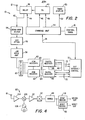
- FIGURE 1 illustrates a perspective view of the overall seismic telemetry system;
- FIGURE.2 illustrates a block diagram of the command station for controlling the remote data acquisition units;
- FIGURE 3 illustrates a block diagram of a remote data acquisition unit;
- FIGURE 4 illustrates a block diagram of the receiver portion of the transceiver on the remote data acquisition unit;
- FIGURE 5 illustrates a block diagram of the transmitter portion of the transceiver on the remote data acquisition unit;
- FIGURE 6 illustrates a schematic diagram of the receiving portion of the transceiver;
- FIGURE 7 illustrates a schematic diagram of the logic circuit for achieving unit synchronization;
- FIGURE 8 illustrates the modulation waveform for modulation of the carrier;
- FIGURE 9 illustrates a schematic diagram of the modulation driver for the transmitter portion of the transceiver;
- FIGURE 10 illustrates an expanded view of the modulation waveform for one bit of data;
- FIGURE 11 illustrates a block diagram of the PCM receiver of the command unit;
- FIGURE 12 illustrates a schematic diagram of the PCM receiver;
- FIGURE 13 illustrates the sequence of bits in both the status words and the data words that are transmitted from the remote data acquisition unit;
- FIGURES 14a-f illustrate a schematic diagram of the digital receiver; and
- FIGURE 15 illustrates timing diagrams for the skew measurement utilizing the update pulses.
- Referring now to FIGURE 1, there is illustrated a perspective view of tpe seismic telemetry system of the present invention. The system comprises a
command station 10 disposed on a solid location with anantenna 12 attached thereto for operating over a wireless data link. A plurality of remote data acquisition units 14 (hereinafter referred to as "DAU"'s) are disposed at select remote locations from thecommand station 10. Each of the DAU's 14 is comprised of acylindrical body 16 that is operable to support electronics therein and maintain buoyancy at the surface level and anantenna 18 disposed on the portion of thebody 16 that extends above the water. Theantenna 18 is operable to transmit over and receive information from the wireless data link to communicate with thecommand station 10. Thecylindrical body 16 is attached to afloat 20 by acable 22. Thefloat 20 is attached to ananchor 24 through ananchor cable 26, theanchor 24 resting upon asea bottom 28. Ahydrophone 30 also rests on the sea bottom and is attached to theDAU 14 through asensing cable 32. Thehydrophone 30 is operable to sense seismic data in the general location thereof. Although a hydrophone has been illustrated, it should be understood that any seismic transducer may be used, such as a geophone. - The
hydrophones 30 that are attached to the DAU's 14 are laid along a seismic line such that a plurality of data points can be obtained at predetermined distances. Thehydrophones 30 are then connected to an associated one of the DAU's 14. The distance between adjacent ones of the DAU's 14 is in the range of from 10 to 100 meters. At this spacing, the distance between thecommand station 10 and the string of DAU's 14 can be up to 10 miles, but this depends upon the particular layout utilized. - Each
DAU 14 transmits and receives over the data link, which is a radio frequency (RF) data link for reception at thecommand station 10 in order to communicate with thecommand station 10. Since eachDAU 14 transmits data received from aseparate hydrophone 30, it is necessary to distinguish the DAU's 14 at thecommand station 10. This is accomplished by utilizing discrete channels in the RF spectrum associated with each of the DAU's 14. In order to preserve dynamic range and the signal to noise ratio in the transmission system, it is necessary to have a transmission system that utilizes appropriate modulation techniques and bandwidth conservation techniques to operate in a given.portion of the frequency spectrum. In the preferred embodiment, the system occupies the RF frequency spectrum from 72 MHz to 76 MHz. Although much wider portions of the spectrum can be utilized, it is not practical to do so since overcrowding of the spectrum is severe in certain areas and only certain portions are relatively free for general use. As there are many factors to consider when choosing a frequency band to operate in, such as cost, transmission properties at certain wavelengths, power efficiencies and circuit realization techniques, the practical constraints of developing a wireless telemetry system normally result in utilization of a very small portion of the spectrum, resulting in a very narrow overall system bandwidth. - In a normal seismic data acquisition system, anywhere from 72 to 240 hydrophones may be utilized. Since each hydrophone is associated with a
separate DAU 14, a discrete channel must be reserved for each hydrophone/DAU combination. Therefore, up to 240 channels may have to be accommodated in the 4 MHz bandwidth. As will be described hereinbelow, this is achieved by utilizing the appropriate modulation technique in conjunction with various bandwidth conservation techniques. - Referring now to FIGURE 2, there is illustrated a block diagram of the
command station 10. Thecommand station 10 is comprised of acommand unit 34 which has acontrol panel 36 connected thereto. Thecommand unit 34, as will be described hereinbelow, is operable to generate a plurality of commands that control both transmission and reception by theantenna 12 and the transmission and reception of the DAU's 14. Theantenna 12 is connected to one port of arelay 38 and atransmitter 40 has the output thereof connected to another port of therelay 38. Therelay 38 is operable in the transmit mode to receive a signal from thetransmitter 40 and output it to theantenna 12 and, in the receive mode, to receive an RF signal from theantenna 12 and route it to anoutput port 42 on therelay 38. Theoutput 42 comprises the received data. Acontrol line 44 is connected between the command unit and therelay 38 to provide the control signal therefore to determine whether the relay is in the transmit mode. Thetransmitter 40 has data input thereto through adata line 46 and control signals therefor are input through acontrol line 48.TheTcommand unit 34 determines the data which is to be modulated onto thetransmitter 40 and inputs this data along theline 46 and, in addition, determines whether thetransmitter 40 is to be activated by signals on thecontrol line 48. Atimer display 50 is also connected to thecommand unit 34 through a signal line 52 to measure the on time of the DAU's 14. - The receive signal on the
relay 38 is passed through the receive port to a bandpass filter. Thebandpass filter 54 is generally a system filter that rejects all frequencies outside of the operating band that is allocated to the system, and passes all frequencies within the band with minimal insertion loss therein. Thefilter 54 prevents large extraneous signals from degrading the dynamic range of the system. The output of the bandpass filter is input to avariable attenuator 56 to select an attenuation therefor. Thevariable attenuator 56 allows the dynamic range, of the system to be adjusted such that RF signals from all of the DAU's 14 can be attenuated. High RF levels may result from the command station being disposed relatively close to the seismic data line. The output of the variable attenuator is then input to a low noise amplifier (LNA) 58 to prevent successive system elements from severely degrading the system sensitivity. - The output of the
LNA 58 is input to apower divider 60 which divides the signal output by theLNA 58 to a plurality of output ports. Since each of the DAU's 14 operates on a discrete channel at a discrets frequency, it is necessary to provide a discrete receiver for each of the DAU's 14. This is accomplished with thepower divider 60. Thepower divider 60 merely provides a means for dividing the power while maintaining the correct impedence match and, in addition, provides some isolation from channelito channel. - Each of the plurality of outputs of the
power divider 60 is connected to an individual pulse code modulation (PCM)receiver 62. Each of thePCM receivers 62 is tuned to one of discrete frequencies for receiving the transmitted data from the associated one of the DAU's 14. ThePCM receiver 62 selects the appropriate frequency, demodulates the carrier and decodes the data. The output of thePCM receiver 62 consists of PCM data. This data is transmitted along a PCM data signalline 64 as a digital bit stream to adigital receiver 66. Thedigital receiver 66 obtains synchronization with the serial bit stream and outputs the proper sequence of digital words that represent the digital data. The digital words are output on adata bus 68 that is multiplexed between thedigital receivers 66 that are associated with each of thePCM receivers 62. Thedata bus 68 is also connected to an external'storage/control device 70 that is operable to store the data output by thedigital receiver 66 and also output control signals for various functions, as will be described hereinbelow. These various other functions are either output as part of thedata bus 68 or on signal lines 72. The external storage/control device 70 is in communication with thecommand unit 34 through a signal line 74. - Referring now to FIGURE 3, there is illustrated a block diagram of the
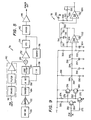
DAU 14. Theantenna 18 is connected to a transmit/receive (T/R) switch 76 to selectively connect atransmitter 78 or areceiver 80 to theantenna 18. When thetransmitter 78 is connected to theantenna 18, encoded data is transmitted over the data link to thecommand station 10 and, when thereceiver 80 is connected to theantenna 18, data from thecommand station 10 is received by theDAU 14. - A
power supply 82 is provided to provide power to theDAU 14. This is normally in the form of batteries. Thepower supply 82 is connected to apower control circuit 84 which controls the distribution of power from thepower supply 82 to the various components on the board. As will be described hereinbelow, each of the DAU's 14 has various modes which, in order to conserve power, do not operate at all times. Ananalog circuit 86 is connected to thepower control board 84 for control thereof and to an analog input which is connected to thehydrophone 30. Theanalog circuit 86 basically processes the analog data. Alogic control circuit 88 contains the internal clock of theDAU 14 and the processing circuitry to convert the analog signal into digital words. This is accomplished with an analog to digital (A/D) converter which converts samples at the sampling rate required to obtain the proper system response. The analog data is digitized to the desired resolution and in the appropriate format for input to thetransmitter 78. - The
logic control circuit 88 is connected to theanalog circuit 86 throughsignal lines signal line 94 to thetransmitter 78 for modulation on the RF carrier. Data received by thereceiver 80 is input to thelogic control circuit 88 on asignal line 96. Acontrol line 98 is connected between thelogic control circuit 88 and thepower control circuit 84 to provide signals therebetween such that thereceiver 80 andtransmitter 78 can be controlled. To conserve energy in thepower supply 82 and to prevent interference between thetransmitter 78 and thereceiver 80,control lines transmitter 78 andreceiver 80, respectively, from thecontrol circuit 84. Thecontrol circuit 84 controls the power thereto such that thetransmitter 78 is turned on only during transmission of data and thereceiver 80 turned off during that time whereas thereceiver 80 is turned on only during reception from the data link with thetransmitter 78 turned off at that time. For power conservation purposes, thetransmitter 78, which has a relatively higher power consumption than other components in theDAU 14, is only turned on when required. However, thereceiver 80 does not require that much standby power but interference considerations may require that it be turned off during transmission of data. - Referring now to FIGURES 1-3, the general system operation will be described. To conserve power, the DAU's 14 have a standby mode and a data mode. In the standby mode, part of the
receivers 80 are turned on to "listen" to the data link for a transmission. In the preferred embodiment, all of the DAU's 14 have theirreceivers 80 tuned to a single frequency. In this manner, they are all "listening" for the same signal. This signal is transmitted by thecommand station 10 to indicate to all of the DAU's 14 that data is about to be taken. Since the data taken by thehydrophones 30 is normally in response to an artificially created seismic shock, it is not necessary to have the DAU's 14 running until just prior to creation of the shock. When thereceiver 80 receives the initial signal, the remaining portions of each of the DAU's 14 are put into a "data ready" mode. In this mode, the DAU's 14 are able to receive various types of data indicating to them the manner in which they are to operate such as the time interval over which the DAU's 14 operate, when they should "power up" and when they should transmit data. After a signal is received from thecommand station 10 to prepare the DAU's 14, portions thereof are activated such that power is provided to the appropriate circuits to transmit data. As will be described hereinbelow, a status code is initially sent by eachDAU 14 to indicate to thecommand station 10 various parameters of theDAU 14 such as internal voltages, unique code numbers and even indications that the internal battery has a low voltage level or that water is inside thecylindrical body 16 of theDAU 14. This status signal is transmitted for approximately 1 to 10 seconds and then the data is transmitted in a serial bit stream. This digital bit stream will continue for the time interval that was originally input to each of the DAU's 14. The data received as digital words is then recovered from the RF carrier and stored in the external storage/control 70 of thecommand station 10 for later analysis. If the data is to be stored on a magnetic storage medium, the format utilized for this data storage is determined by the Society of Exploration Geophysicists and it is a standard format of storage. However, the data may be stored in any storage medium. - Referring now to FIGURE 4, there is illustrated a block diagram of the
receiver 80 on theDA U 14. Alow noise amplifier 104 has the input thereof connected to the antenna.l8 and the other end thereof connected to the RF input of amixer 106. A crystal controlledoscillator 108 has the output thereof connected to the local oscillator input of themixer 106. The output of themixer 106 is connected to the input of an intermediate frequency (IF)amplifier 110. The gains of theamplifiers antenna 18 and received on the input of theamplifier 104. The output of theIF amplifier 110 is input to an IFfilter 112 that is typically centered at a frequency of 10.7 MHz, which is a standard frequency in the communications industry. After processing by the filter, the signal is input to ademodulator 114. Thisdemodulator 114 demodulates the data from the RF carrier. In the preferred embodiment, the data that is encoded on the RF carrier transmitted from thecommand station 10 is dual tone multi-frequency (DTMF) data. This data is input to either aDTMF decoder 116 or areset decoder 118. The DTMF decoder receives the DTMF data and outputs a signal corresponding thereto. Thereset decoder 118 tone decodes the signal and generates reset pulses, the operation of which will be described hereinbelow. It should be understood that any modulation system that can provide information as to a number of parameters to control the various DAU's 14 would be acceptable. - In the preferred embodiment, the
command station 10 transmits a signal on a frequency of approximately 73 MHz, which is in the middle of the system band, and which is received simultaneously by all of the DAU's 14. In this manner, all DAU's 14 can be controlled. Although not shown, it should be understood that the DAU's 14 can be coded for selective control thereof such that only individual ones of the DAU's 14 will be turned on or, alternately, groups of DAU's 14 can be selectively turned on. This would allow a higher degree of versatility in collecting seismic data. - Referring now to FIGURE 5, there is illustrated a block diagram of the
transmitter 78 in theDAU 14. Thetransmitter 78 is basically a phase lock loop (PLL) with phase modulation therefore. However, it should be understood that frequency shift key (FSK) modulation can also be used. A reference is provided for the PLL with acrystal reference oscillator 120 which is buffered through abuffer amp 122. The output of thebuffer amp 122 is input to asquaring circuit 124 for shaping the waveform output by thebuffer 122. 'The output of the squaring circuit l24 is input to one input of aphase detector 126. The output of thephase detector 126 is input to aloop filter 130 that provides the proper frequency response for the PLL. The output of theloop filter 130 is input to a summingjunction 128 for summing of a modulation signal with theloop filter 130 output. The output of the summingjunction 128 is input to aloop amplifier 132 which drives aVCO 134. The output of theVCO 134 is input to asquaring circuit 136 for input to adivider 138. Thedivider 138 divides the signal output by theVCO 134 by a factor of 16 and this signal is input to the other input of thephase detector 126 for comparison with the reference signal generated in thereference oscillator 120. Therefore, the frequency of thereference oscillator 120 is equal to the frequency output by thedivider 138 which is the divided frequency of theVCO 134. The filtered output from theloop amp 132 comprises the error signal that sets the frequency output by theVCO 134. This error signal is modulated by a modulation signal that is input to the summingjunction 128 from amodulation driver 140. This modulates the phase of theVCO 134 to provide a phase modulated output. The output from theVCO 134 is input to adriver 142 to provide power amplification thereof and the output of thedriver 142 is input to apower amp 144 to provide the output power for theDAU 14. - By utilizing a VCO at the crystal frequency and modulating the input thereof, a more stable output frequency with fewer out of band harmonics can be achieved. Other techniques, such as multiplying the frequency output of a stabilized reference source or mixing two frequencies together, require a large number of filters to remove unwanted harmonics thereof. By utilizing the phase lock loop technique, it is possible to use a reference oscillator having a much lower frequency, thereby allowing the use of a lower frequency crystal therein to provide more stability. The crystal in the
reference oscillator 120" is selectable to determine the output frequency of theVCO 134. By changing this crystal, one of the discrete channels allocated for operation of the DAU's 14 can be selected. - Referring now to FIGURE 6, there is illustrated a schematic diagram of the
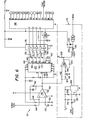
DTMF decoder 116 and thereset decoder 118. The reset decoder l18 is shown within the phantom lines. The output of thedemodulator 114 of thereceiver 80 is termed DEMOD DATA. The DEMOD DATA is input to anoperational amplifier 146 through a series connectedresistor 148. The positive input of theamplifier 146 is connected to ground through aresistor 150. Hereinafter, grounds are referred to a reference level and shall be illustrated by the conventional symbol. therefor. Acapacitor 152 is connected in parallel to theresistor 150. The power supply terminal of theamplifier 146 is connected to a voltage V1 and the negative voltage input thereof is connected to ground. Aresistor 154 has one end thereof connected to the positive input of theamplifier 146 and the other end thereof connected to V1. Aresistor 156 has one end thereof connected to the output of theamplifier 146 and the other end thereof connected to the negative input of theamplifier 146. Acompensation capacitor 158 is connected to the compensation inputs of theamplifier 146. Theamplifier 146 is configured as an inverting amplifier for providing some amplification of the demodulated signal and acting as a buffer therefor. - The output of the
amplifier 146 is input to a .DTMF converter 160. The DTMF converter converts the DTMF signals that were demodulated from the received carrier into digital signals on the output thereof. Acrystal 162 is provided for a time base reference thereof. The components attached to theDTMF converter 160 and the connection therefore are described in Silicon Systems SSI 201 data sheet. TheDTMF converter 160 has fourdigital outputs hex level converter 176 for converting the input level to an appropriate-logic level on the output thereof. Thehex converter 176 has the reference input thereof connected to ground and the supply input thereof connected to a level V2. The logic level on the output of thehex converter 176 is set to the level V2. Pull downresistors - The converted levels of the lines 164-170 are input to the A, B, C and D inputs, respectively, of a 4-
l6 line decoder 186. The 4-16 decoder is operable to decode the four-bit digital word on the input thereof to activate one of 16 ouputs therefrom. In this manner, the DTMF signal that was transmitted to thereceiver 80, can carry up to 16 separate bits of information that activate a selected one of the outputs of thedecoder 186. ANAND gate 188, the input of which is connected to an output of theDTMF converter 160 through one of the level converters on thehex converter 176, has the output thereof connected to the inhibit input of thedecoder 186. This inhibit input outputs a "high" logic state on all of the outputs of the 4-16decoder 186 when activated. - The output of the
amplifier 146 having the buffer demodulated signal thereon is connected to the negative input of anoperational amplifier 190 through aresistor 192 and to the positive input thereof through tworesistors capacitor 198 has one end thereof connected to the common connection between theresistors feedback resistor 200 is connected between the output of theoperational amplifier 190 and the positive input thereof. Theamplifier 190 and the associated components therefor is operable to provide a squaring function to shape the input signal therefor. A pull-upresistor 202 has one end thereof connected to the output of theamplifier 190 and the other end thereof connected to V 2 or V 3 to provide a current source therefore. - A NAND gate 204 has one input thereof connected to the output of the
amplifier 190 and the other input thereof connected to the output of atimer 206. Atiming resistor 208 is provided with one end thereof connected to the timing_input of thetimer 206 and the other end thereof connected to V2 or V3. Atiming capacitor 210 has one end thereof connected to the timing input of thetimer 206 and the other end thereof connected to ground. Theresistor 208 and thecapacitor 210 are operable to provide a timing function for thetimer 206 which, in the configuration illustrated, is configured as a one-shot circuit. The trigger input of thetimer 206 is connected through acapacitor 212 to one of the outputs of the 4-16decoder 186. Aresistor 214 has one end thereof connected to the trigger input and the other end thereof connected to V 2 or V3. Thecapacitor 212 and theresitor 214 function to differentiate the output of the 4-16decoder 186 to provide a trigger pulse. The output selected from thedecoder 186 is labeled SYNC DECODE. In the preferred embodiment, the interval of the pulse output by the timer 206' is approximately 300 millisec. The output of the NAND gate 204 is connected to both inputs of aNAND gate 216 through acapacitor 218. A resistor 220 has one end thereof connected to the input of theNAND gate 216 and the other end thereof connected to V2. Adiode 222 has the anode thereof connected to the input of theNAND gate 216 and the cathode thereof connected to V2. Thecapacitor 218, the resistor 220 and thediode 222 function as a pulse converter that converts the transitions on the output of the NAND gate 204 to a series of narrow width pulses that occur for each transition and are inverted by theNAND gate 216. Therefore, a sine wave that is input to theamplifier 190 results in a plurality of narrow pulses output by theNAND gate 216. These pulses are referred to as the SYNC signal. - During the receive mode of the
DAU 14, power is supplied such that the voltage reference Vl, V2 and V3 are supplied to the circuit. TheDTMF converter 160 receives the DTMF signals and derives the coded four-bit word therefrom. This four-bit word contains information that is input to thelogic control circuit 88 on theDAU 14 through activation of the outputs of thedecoder 186. Prior to the transmission of data, it is necessary to program all of the DAU's 14. Initially, each of the DAU's 14 is in a standby mode and must be instructed to energize the decoder and logic circuits thereof. After theDAU 14 has received the signal to ready itself for further data, the time that the DAU is to collect and transmit data is then sent to theDAU 14 in the form of a sequence of DTMF codes and CLEAR codes. Prior to transmission of data, it is necessary to synchronize all of the DAU's 14, as will be described hereinbelow. After synchronization, signals are sent to the DAU's 14 to indicate the mode of operation, either STATUS or DATA, that the DAU is to be in. - To synchronize the
DAU 14, a DTMF signal is sent to thereceiver 80 that is decoded and input to thetimer 206. Once thetimer 206 has been initiated, it opens the gate 204. A tone is then transmitted by thecommand station 10 and is input to theamplifier 190 for shaping thereof. This tone, in the preferred embodiment, has a frequency of 250 Hz, 500 Hz, or 1 KHz. As described above, this tone is converted into a series of narrow pulses having a frequency equal to the tone input to theamplifier 190. - Referring now to FIGURE 7, there is illustrated a schematic diagram of the clock generation circuit that receives the SYNC signal from the
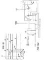
reset decoder circuit 118. Each of the DAU's 14 has a system clock that is disposed on thelogic control circuit 88..This reference oscillator has a crystal reference that is common to all of the DAU's 14. This crystal reference is utilized to generate a relatively high frequency clock; in the preferred embodiment, this frequency is around 2.3 MHz which is divided down to provide an intermediate frequency. This oscillator is indicated by thereference oscillator 222 in FIGURE 7. The output of thereference oscillator 222 is input to the clock inputs of three programmable four-bit counters 224, 226 and 228. The Carry Out of thecounte 224 is connected to the Enable inputs of thecounter 226 and the Carry Out of thecounter 226 is input to the Enable input of thecounter 228. Therefore, thecounters - The Q3 and Q4 outputs of the
counter 224 are connected to two inputs of a threeinput NAND gate 230. The other input of theNAND gate 230 is connected to the Ql output ofcounter 226. The output ofNAND gate 230 is input to one input of a threeinput NAND gate 232. The Q2, Q3 and Q4 outputs ofcounter 226 are inverted byinverters gate 240. The output of the NORgate 240 is input to one input of theNAND gate 232. The Ql and Q2 outputs of thecounter 228 are input to both inputs of a NORgate 242, the output of which is input to the third input of theNAND gate 232. The output of theNAND gate 232 is input to one input of aNAND gate 244, the other input of which is connected to the Q2 output ofcounter 226. The output of theNAND gate 244 provides the sample rate at which the data is sampled by the A/D converter on the logic board, (not shown). - The SYNC signal is input to the reset inputs of the
counters NAND gate 244. When a pulse is present on the CLEAR input of the counters 224-228, all the outputs will be at a logic "low". After the pulse is removed, the output of thereference oscillator 222 will clock the counters 224-228 through their sequence. The reset pulses are not synchronized with thereference oscillator 222 and, therefore, they can occur at any phase of thereference oscillator 222. It is the trailing edge of the pulses that allows the counters 224-228 to begin counting. However, they do not begin counting until they receive a transition from thereference oscillator 222. There-fore, all of the counters 224-228 in all of the DAU's 14 will begin counting upon the next transition of their internal reference clocks. This will constitute the total error for all of the DAU's 14 at initiation of the counters 224-228. However, after the reset pulses are removed, all of the counters drift as a function of the drift in theoscillators 222. In the preferred embodiment, the internal crystal reference of 2.3 MHz is divided down to approximately 576 KHz. One period of the 576 KHz clock will therefor be the maximum error for the initial count between all counters on all DAU's 14. - Since the reset pulses have a frequency equal to the sample rate output by
NAND gate 244, the count will always initiate a defined number of clock periods after each reset pulse on the CLEAR input. Therefore, if aparticular DAU 14 misses one of the reset pulses due to poor reception, the maximum error between thisDAU 14 and other DAU's 14 is the drift of itsinternal reference oscillator 222 for one period (or the number of periods missed) of the sample rate. - Referring now to FIGURES 8 and 10, there are illustrated the waveforms representative of the modulation technique used in the
transmitter 78 in each of the DAU's 14. Awaveform 246 represents a portion of a digital word that is to be transmitted over the data link. A "low" logic state is represented by a "0" and a "high" logic state is represented by a "1". These logic states occur at a given bit rate which is the frequency at which the individual bits of logic information are transmitted. One "bit time" is equal to the duration of a particular bit. Awaveform 248 represents the format in which the digital data is encoded. In the preferred embodiment, this format is a non-return to zero (NRZ) format. The occurrence of a logic "1" results in a transition in the NRZ data from either a logic low to a logic high or a logic high to a logic low. For example, a continuous string of logic "1"'s would result in a continuous string of transitions between the successive bits of data. However, a logic "1" followed by a logic "0" would result in no transition and a string of logic "0"'s would result in no transitions either. The data represented by thewaveform 248 is the PCM data that is input to themodulation driver 140 on thetransmitter 78 and the output of themodulation driver 140 that is input to the summing junction.128 is represented by awaveform 250. Since the transmission of a sharp transition would require a fairly wide bandwidth and such a signal would be very harmonic rich, it is necessary to filter the signal to minimize the required bandwidth without losing the digital information. With the NRZ format, it is only necessary to detect that a transition has occurred within a given bit time. Therefore, the signal in thewaveform 248 is filtered by themodulation driver 140 such that the transition between two logic states is very "soft", that is, the signal requires the entire duration of a particular bit to make the transition. This minimizes the rate of change of the transition for that duration. For example, the occurrence of adigital bit 252, which is a logic "1", results in a transition 254 from a logic low to a logic high state in thewaveform 248. This transition is filtered by themodulation driver 140 and is represented by afilter transition 256 on thewaveform 250. The occurrence of anotherdigital bit 258 results in the opposite transition 260 on thewaveform 248 from a logic high to a logic low state. This results in a filteredtransition 262 on thewaveform 250. As illustrated in thewaveform 250, both the filteredtransitions - Referring further to FIGURE 9, there is illustrated a schematic diagram of a
modulation driver 140. The PCM data is input to the base of anNPN transistor 264 through a series connectedresistor 266. Thetransistor 264 has the emitter thereof connected to ground and the collector thereof connected to +V through aseries resistor 268. The PCM data is also input to the base of anNPN transistor 270 through aseries resistor 272. Thetransistor 270 has the emitter thereof connected to ground and the collector thereof connected to +V through aresistor 274. Thetransistor 264 has the collector thereof connected to the base of aPNP transistor 276 through aseries resistor 278 and thetransistor 270 has the collector thereof connected to the base of anNPN transistor 280 through aseries resistor 282. Thetransistor 280 has the emitter thereof connected to ground and the collector thereof connected to the collector of thetransistor 276. Thetransistor 276 has the emitter thereof connected to +V. Thetransistors - The collector of the
transistor 280 is connected to one end of aresistor 284, the other end of which is connected to anode 286. Aresistor 288 has one end thereof connected to thenode 286 and the other end thereof connected :to +V. Resistor 290 has one end thereof connected to ground and the other end thereof connected to thenode 286. A capacitor 29-2 has one end thereof connected to ground and the other end thereof connected to thenode 286. Aresistor 294 has one end thereof connected to thenode 286 and the other end thereof connected to anode 296. Acapacitor 297 has one end thereof connected to ground and the other end thereof connected to thenode 296. Theresistors resistor 294 and thecapacitor 297 form another section of a filter. The combined sections of the filter form a low pass function that filters the leading edge of each of the transitions for the PCM data. - The output of the filter sections at the
node 296 is connected to the negative input of an operational amplifier. 298 through aresistor 300. Aresistor 302 and acapacitor 304 have one of the ends thereof connected to the positive input of theamplifier 298 and the other end thereof connected to ground. Aresistor 306 has one end thereof connected to the positive input of theamplifier 298 and the other end thereof connected to +V.A feedback capacitor 308 has one end thereof connected to the negative input of theamplifier 298 and the other end thereof connected to the output of theamplifier 298. Aresistor 310 and aresistor 312 have one of the ends thereof connected to anode 314. The other end of theresistor 310 is connected to the negative input of theamplifier 298 and the other end of theresistor 312 is connected to the output of theamplifier 298. A capacitor 316 has one end thereof connected to thenode 314 and the other end thereof connected to ground. Thenode 314 is connected to the positive input of anoperational amplifier 318 through aresistor 320. The negative input of theamplifier 318 is connected to anode 322. Aresistor 324 has one end thereof connected to thenode 322 and the other end thereof connected to one end of avariable resistor 326. The other end of thevariable resistor 326 is connected to the output of theamplifier 318. Aresistor 328 has one end thereof connected to thenode 322 and the other end thereof connected to one end of acapacitor 330. The other end of thecapacitor 330 is connected to ground. Theamplifier 298 and theamplifier 318 havecompensation capacitors - The
amplifier 298 and thecapacitor 308 form an integrator for integrating the output signal of the two section filter atnode 296. Theresistor 312 and the capacitor 316 form a one section low pass filter to filter the output of the integrator. This one section filter essentially delays the signal. Theresistor 310 feeds back a portion of output signal for summation at the input of theamplifier 298. Basically, the two section filter "rolls off" the end of the transition and the integrator in combination with the one section filter rolls off the initial portion of the transition. - Referring now to FIGURE 10, there is illustrated a waveform representative of one transition of the
waveform 248 of FIGURE 8. A waveform 336 (phantom outline) illustrates the original transition and awaveform 338 illustrates the filtered waveform. The filtered waveform:338 is comprised of three transitions. Since it is necessary to make a transition from alow logic level 340 to ahigh logic level 342, it is necessary to undergo a rate of change for the waveform, that is, the derivative thereof must increase to a maximum rate of change and then decrease to a value of zero. For a step function, as shown in thewaveform 336, the derivative would be essentially infinite for a short duration of time. It if this high rate of change that requires the very large bandwidths to reconstruct the data at the receiver. Thewaveform 338 reduces the required bandwidth by forming afirst portion 344 that undergoes an increasing rate of change until a constant rate of change is achieved at thepoint 346. This is a constant rate of change for thewaveform 338 which is maximum at that point and begins decreasing over a portion of thewaveform 338. To achieve the minimum bandwidth for a given transition, thewaveform 338 must have a rate of change that approaches that of a sine wave. Since a sine wave has only one fundamental frequency, the bandwidth required for transmission thereof is minimal depending upon the frequency. - The circuit of FIGURE 9 realizes the
waveform 338. The input pulse is filtered by the two filter sections preceding thenode 296 such that the leading edge is "rolled off", that is, the portion of thewaveform 348 is formed with an evenly decreasing rate of change. However, the leading edge still undergoes a very rapid rate of change prior to integration thereof. This portion of the curve is integrated by theamplifier 298 and the associated circuitry. The integration function decreases the overall rate of change for the transition. Eowever, the rate of change at the initiation of integration is relatively high since the signal level changes from a constant level to sloping curve very abruptly. This abrupt change results in very high harmonics. To alleviate this, the one section filter and thefeedback resistor 310 operate to put a delay in the circuit. This delay causes theinitial portion 344 of thewaveform 338 to change at a slower rate, i.e., that of a sine wave. By selecting the values properly, the curve of FIGURE 10 can be realized. The values for the circuit of FIGURE 9 for a bit width of 110 microseconds are included in Table 1 as follows:
- Referring now to FIGURE 11, there is illustrated a block diagram of the
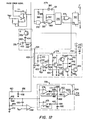
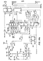
PCM receiver 62 in thecommand station 10. As described above, the PCM receiver . 62 receives the modulated RF carrier and demodulates the carrier to retrieve the NRZ data. The RF data is input to the input of anRF amplifier 350 for amplification and the amplified output thereof is input to the RF input of amixer 352. Alocal oscillator 354 has the output thereof connected to the local oscillator input of themixer 352. Thelocal oscillator 354 is a voltage controlled crystal oscillator (VCXO) having acrystal 356 attached thereto to provide the reference therefor. The output of themixer 352 is input to an IFfilter 358 having a frequency of 10.7 MHz. The output of this filter is input to an IFamplifier 360 for amplification thereof. The output thereof is input to adivider circuit 362 to divide the output thereof by a factor of approximately 8. The divided output is input to one input of aphase detector 364 and the output of acrystal reference oscillator 366 is connected to the other input of thephase detector 364. Thereference oscillator 366 has acrystal 368 attached thereto to provide a stabilized reference therefor. The output of thephase detector 364 is input to avariable loop filter 370, the output of which is input to aloop amplifier 372. The output of theloop amplifier 372 provides the phase error voltage for thelocal oscillator 354. Thephase detector 364,reference oscillator 366,loop filter 370 andlocal oscillator 354 form a phase lock loop (PLL) for locking to the received signal. Normally, phase lock loops have a particular frequency range over which they can capture a.particular frequency and a certain range of phase error that they can lock to. Since, as described above, there are a plurality ofPCM receivers 62 operating on discrete channels, it is necessary that the frequency capture range of the PLL be minimized such that it does not lock to an adjacent channel. This is achieved by utilizing a VCXO for thelocal oscillator 354 that will not lock over a large range of frequencies. - To adequately demodulate the PCM data modulated on the RF carrier, it is necessary to provide a transfer function for the
loop filter 370 that will adequately demodulate the data. However, one of the.disadvantages to having a sufficient loop filter is that the "lock time" for the PLL is substantially decreased. This is a disadvantage when the loop goes out of lock due to noise pulses or upon initiating lock. To alleviate this, theloop filter 370 has a second mode in which the lock time is increased. This is achieved by detecting lock with alock detector 374 having the input thereof connected to the output of thephase detector 364 and the output thereof connected to a control input for theloop filter 370. Lock is determined by the relative phase error with respect to the phase of thelocal oscillator 354. When the phase error between the IF signal and thereference oscillator 366 exceeds a predetermined value, the lock detector outputs a signal to change the lock time of the PLL. This allows lock to occur at a faster rate, thereby reducing loss of data. If this lock time were not increased, it is possible that a number of bits of the data would be lost. - The output of the
phase detector 364 is input to a filter 377 and then the demodulated data is input to abase line tracker 379 to remove low frequency components therefrom. This base line tracker is necessary since the logic state of the data received is determined by sensing a transition from a low logic level to a high logic level. This is accomplished by measuring the signal level with respect to a reference. If low frequency components exist, this introduces substantial error. - Referring now to FIGURE 12, there is illustrated a schematic diagram of the portion of the PCM .
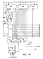
receiver 62 for processing the IF signal output by theIF amp 360 to provide the phase error signal for thelocal oscillator 354. The schematic of FIGURE 11 also includes the schematic for the demodulator 377 and thebase line corrector 379. The output of theIF amplifier 360 in FIGURE 11 is input into thedivider 362. The output signal from theamplifier 360 is designated IF SIG. Thedivider 362 is a four-bit binary counter which divides the IF SIG by a factor of 8. The IF SIG is input to the reset input thereof and the output taken from the QD output thereof. The output is input to one input of an Exclusive NORgate 375. - A
NAND gate 378 has both inputs thereof connected to one side of acrystal 380 and the output thereof connected to one side of acapacitor 382. A capacitor 384 is connected between the input of theNAND gate 378 and ground. The other end of thecapacitor 382 is connected to both inputs of aNAND gate 388. Aresistor 390 has one end thereof connected to the input of thegate 388 and the other end thereof connected to the output of thegate 388. Acapacitor 391 has one end thereof connected to the output of thegate 388 and the other end thereof connected to the other end of thecrystal 380. Thegates crystal 380 comprise a reference oscillator for providing a reference signal. This reference signal is input to adivider 392 that divides the signal by a factor of 2 for input to the other input of the Exclusive NORgate 375. The output of .the divider has a frequency of approximately 1.35 MHz and the Exclusive NORgate 375 compares the phase of the signal to the phase of the IF SIG that was divided by a factor of 8 by thedivider 362. The output of the Exclusive NORgate 375 is the phase detected signal and this signal is input to anode 394. Theloop filter 370 has the input thereof connected to thenode 394 for providing the PLL loop response. - The
loop filter 370 has aresistor 399 with one end thereof connected to thenode 394 and the other end thereof connected to anode 398. Theresistor 399 and thecapacitor 400 provide the secondary or fast loop filtering for the loop. This portion of theloop filter 370 provides a loop response that obtains lock during initial.lock up. This fast loop is necessary when large phase errors exist in order to acquire lock at a faster rate. The primary or slow loop response that is utilized to demodulate the data is accomplished by placing a series connectedresistor 402 andcapacitor 404 having one end thereof connected to thenode 398 and the other end thereof connected to the collector of anNPN transistor 406. The emitter of thetransistor 406 is connected to ground and the base thereof is connected to the output of thelock detector 374. When theseries resistor capacitors transistor 406, the loop response of the PLL is altered such that the rate of lock acquisition is decreased. The point at which thistransistor 406 is activated is determined by thelock detector 374 which has its input thereof connected to thenode 394. - A
lock detector 374 has aresistor 408 andcapacitor 410 connected as an L section filter with the other end of the capacitor connected to ground. Aseries capacitor 412 has one end thereof connected to the output of the L-section filter and the other end thereof connected to the input of anoperational amplifier 414 through aseries resistor 415. The output of theamplifier 414 is connected to the base of aPNP transistor 416 through aseries resistor 418. Afeedback resistor 420 is connected between the negative input of theamplifier 414 in the output thereof. A reference voltage is connected to the positive input of theamplifier 414 through aseries resistor 422. The base of thetransistor 416 is biased to a predetermined level by a voltage divider formed of tworesistors resistor 426 having one end thereof connected to ground. Thetransistor 416 has the emitter thereof connected to +V and the collector thereof connected to the base of aPNP transistor 428. Thetransistor 428 has the emitter thereof connected to +V and the collector thereof connected through a resistor 430 to ground. The output of theamplifier 414 is connected to the base of aPNP transistor 432 through aseries resistor 434 with a resistor 436 having one end thereof connected to the base of thetransistor 432 and the other end thereof connected to ground. The collector of thetransistor 432 is connected to +V through a resistor 440. Adiode 442 has the anode thereof connected to the collector of thetransistor 428 and the cathode thereof connected to the base of anNPN transistor 444. Adiode 446 has the anode thereof connected to the collector of thetransistor 432 and the cathode thereof connected to the base of thetransistor 444. Aresistor 448 has one end thereof connected to the base of thetransistor 444 and the other end thereof connected to ground. The collector of thetransistor 444 is connected to +V through aresistor 450. Aresistor 452 and acapacitor 454 are connected as an L-section filter with thecapacitor 454 thereof having one end connected to ground and aresistor 452 having one end thereof connected to the collector of thetransistor 444. Aseries resistor 456 has one end thereof connected to the output of the L-section filter and the other end thereof connected to the input of thetransistor 406 on theloop filter 370. Thetransistor 444 is the output transistor for thephase lock detector 374. - The
lock detector 374 is operable to control theloop filter 370 when the phase error out of thephase detector 364 exceeds a value that is higher or lower than a predetermined value. These predetermined values are set by voltage dividers. One direction of the error is controlled by thePNP transistors resistors diode 442 conducts current to theresistor 448, thus biasing thetransistor 444 into a conducting state. This results in a low voltage input to the base of thetransistor 406 thereby preventing conduction therein. When the voltage output by theamplifier 414 increases due to an increase in the phase error, the current through theresistor 426 increases thereby cutting.off thetransistor 416, resulting intransistor 428 going into cut off. This eliminates current supplied through theresistor 448 from thediode 442. This increase in voltage on the output of theamplifier 414 also increases the voltage on the base of thetransistor 432 thereby placing the anode of thediode 446 at a ground potential and reducing any current contribution to theresistor 448 therefrom. Therefore, an increase in phase error voltage that raises the output of the voltage of theamplifier 414 turns off thetransistor 406 in theloop filter 370. When the voltage in the output of theamplifier 414 drops, thetransistor 406 begins to conduct and place theresistor 402 andcapacitor 404 in the loop filter circuit. - The signal on the
node 394 when the loop has acquired lock comprises the PCM data. Aresistor 456 has one end thereof connected to thenode 394 and the other end thereof connected to one end of acapacitor 458, the other end of which is connected to ground. Aresistor 460 has one end thereof connected to the junction of theresistor 456 and thecapacitor 458 and the other end thereof connected to anode 462. Aresistor 466 has one end thereof connected to thenode 462 and the other end thereof connected to the negative input of theamplifier 468. Acapacitor 470 has one end thereof connected to the negative input of theamplifier 468 and the other end thereof connected to the output of theamplifier 468. Acapacitor 472 has one end thereof connected to thenode 462 and the other end thereof connected to ground. The positive input of theamplifier 468 is connected to a voltage reference which, although not shown, is variable. Theamplifier 468 is configured as a low pass active filter, the output of which varies about a DC reference . voltage. - The output of the
amplifier 468 is input to thebase line tracker 379.Base line tracker 379 is comprised of anoperational amplifier 474 and anoperational amplifier 476 configured as peak detectors. Theamplifier 474 has the output thereof connected to the cathode of adiode 478 and the negative input thereof connected to the anode of thediode 478. Theamplifier 476 has the output thereof connected to the anode of adiode 480 and the negative input thereof connected to the cathode of thediode 480. Theamplifier 474 is configured as a negative peak detector and theamplifier 476 is configured as a positive peak detector. Aresistor 482 has one end thereof connected to the cathode of thediode 480 and the other end thereof connected to anode 484. Acapacitor 486 has one end thereof connected to thenode 484 and the other end thereof connected to ground. Aresistor 488 has one end thereof connected to thenode 484 and the other end thereof connected to the positive input of acomparator 490. Aresistor 492 has one end thereof connected to the anode of thediode 478 and the other end thereof connected to a node 494. A capacitor 496 has one end thereof connected to the node 494 and the'other end thereof connected to +V. Aresistor 498 has one end thereof connected to the node 494 and the other end thereof connected to the positive input of thecomparator 490. Aresistor 500 has one end thereof connected to the output of thecomparator 490 and the other end thereof connected to the negative input of thecomparator 490. A resistor 502 has one end thereof connected to the negative input of thecomparator 490 and the other end thereof connected to the output of theamplifier 468. The positive inputs of theamplifiers amplifier 468. A pull up resistor 504 has one end thereof connected to the output of thecomparator 490 and the other end thereof connected to +V to provide a current source therefor. - The PCM data, described above, is a signal that has a filtered transition between the beginning of a bit time and the end of a bit time for a given transition. The transition occurs only upon the occurrence of a logical "1". In a long bit stream, a number of logical "l"'s will appear. The occurrence of these transitions will result in an AC signal that has a base line reference. The.positive and negative peak detectors will detect the positive and negative peaks of the signal. For example, a positive going signal will cause a
diode 480 to conduct and charge thecapacitor 486 through thediode 482. Upon going negative, thediode 480 will not conduct and the charge stored on thecapacitor 486 will remain relatively constant. The negative going peak causes thediode 478 to conduct thereby charging or lowering the potential on one end of the capacitor 496 that is, the value of the negative peak is stored thereon. Theresistor 492 in combination with the capacitor 496 provides a time constant for charging thereof and theresistor 482 in combination with thecapacitor 486 provides a time constant therefor. The voltage stored on thecapacitors 486 and 496 is allowed to equilibrate through theresistors comparator 490 to form a reference voltage therefor. This reference voltage represents the average value for a bit transition independent of the baseline variations. The other input to thecomparator 490 is the PCM data output by theamplifier 468. The output of the comparator represents the difference between the two inputs thereof. Since thecomparator 490 only detects a difference between the two inputs, low frequency components of the PCM data will be extracted from the signal since the reference signal and the positive input of thecomparator 490 tracks these low frequency components. In addition, the comparator 49'0 only triggers on the transition of the PCM data at the average level thereof. This average level is midway between the positive and negative peaks thereof to maximize detected signal to noise. Therefore, the output signal from thecomparator 490 is delayed by one-half bit time and provides a transition at the mid-point of the original PCM data bit time and it is this transition of the PCM data that is detected rather than the presence of "high" or "low" logic levels. - Referring now to FIGURE 13, there is illustrated the format for the digital words that are encoded with data.
Format 506 represents the data sample which is an 18-bit word having 12 bits of mantissa represented by the letter "Q" and the letter "S" for sign. The data word also has 3 bits labeled "G" which are gain bits that are utilized to determine the gain of the analog portion of theDAU 14 in order to reconstruct the data.Framing bits bit 508 is "0" and the predetermined value of the framingbit 510 is "1". Aparity bit 512 is also provided as representative of the parity of the data word. In addition to data words, status words are also transmitted. These status words are, as described above, indicative of the status of theDAU 14 and are transmitted in frames, that is, groups of eight status words. The first status word in each frame that is transmitted is thechannel 0 status word represented by a waveform 514 and the remaining status words that are transmitted are represented by awaveform 516. Both thewaveforms 514 and 516 transmit ten bits for the analog status word which are indicated by the letters "Q" for the bits of data and "S" for the sign of that data. The waveform 514 for thechannel 0 status word has two identifying bits 518 and the remaining status words in the waveform 514 have two identifyingbits 520. These bits are at a predetermined location within the status word and can be sampled to detect whether the word is the first word in the frame or subsequent words thereof. Thechannel 0 word is identified by the bits 518 and both bits are a logic "0" whereas one of the identifyingbits 520 in the remaining analog status words is a logic "1". By sampling the location in these words, proper identification can be made. The status words have framingbits waveform 506 and a parity bit 526. The framingbits - Referring now to FIGURES 14a-f, there is illustrated a schematic diagram of the
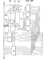
digital receiver 66 of FIGURE 2. Thedigital receiver 66 receives the corrected PCM data output by thebase line tracker 379 of FIGURE 11 and processes this data. The form of the data is an NRZ format in a continuous bit stream, that is, all the bits in each of the sequential digital words are transmitted in a stream of continuous bits. No clock signal is transmitted with the data and, therefore, the clock rate must be recovered and the digital words themselves must be synchronized. The PCM data is input to abuffer 527 which also provides level conversion. The output of thebuffer 527 is input to a D-type flip flop 528 on the data input thereof. The output of theflip flop 528 is input to one input of an exclusive ORgate 530. The other input of thegate 530 is connected to the output of a D-type flip flop 532 which flip-flop also has the data input thereof connected to the output thereof. The clock inputs of theflip flops gate 530 is bi-level coded data. Therefore, theflip flops gate 530 convert the NRZ data to bi-level coded data. - The PCM data output by the
buffer 527 is input to one input of aSchmidt trigger 534 through aseries capacitor 536. The PCM data is also input to aninverter 538 and the inverted signal output therefrom is input to the other input of theSchmidt trigger 534 through aseries capacitor 540. The output of thecapacitor 540 is also connected to +V through aseries resistor 544. The output of theSchmidt trigger 534 is input to the clock input of a D-type flip flop 552 and the output of theSchmidt trigger 548 is input to the reset input of theflip flop 552. Theflip flop 552 has the Q output thereof connected to the data input thereof and the Q output thereof connected to one input of an Exclusive ORgate 554. A D-type flip flop 556 has the Q output thereof connected to the input of aninverter 558 and the Q output thereof connected to the input of aninverter 560. The output of theinverter 560 is connected to the other input of theSchmidt trigger 548 through aseries capacitor 562 and the output of theinverter 558 is connected to the input of aSchmidt trigger 564 through aseries capacitor 566. The other input of theSchmidt trigger 564 is connected to +V. The outputs of thecapacitors - The output of the
Exclusive OR gate 554 is input to the negative input of anamplifier 570 through two series connectedresistors 572 and 574. Acapacitor 576 has one end thereof connected to the junction between the tworesistors 572 and 574 and the other end thereof connected to ground. The positive input of theamplifier 570 is connected to a reference voltage Vref through aseries resistor 578 and the output thereof is connected to the negative input thereof through a series connectedresistor 580 andcapacitor 582. The output of theamplifier 570 is input to one side of a varactor 584 through two series connectedresistors resistors amplifier 570. The varactor is connected to one side of acrystal 592. The other side of thecrystal 592 is connected to one side of avariable inductor 594, which has the other side thereof connected to the base of anNPN transistor 596. The base of thetransistor 596 is connected to ground through aresistor 598. Thetransistor 596 has the collector thereof connected to +V through a resistor 600 and to ground through acapacitor 602, the base thereof connected to +V through a resistor 604 and to ground through two series connectedcapacitors 606 and 608 and the emitter thereof connected to ground through aresistor 610. The emitter is also connected to the negative input of acomparator 612 and to the junction between the twocapacitors 606 and 608. The positive input of thecomparator 612 is connected to one end of a resistor 614, the other end of the resistor 614 being connected to one end of acapacitor 616. The other end of thecapacitor 616 is connected to ground. A resistor 618 has one end thereof connected to the other-end of the resistor 614 and the other end thereof connected to the emitter of thetransistor 596. The output of thecomparator 612 is input to the clock input of a D-type flip flop 620, theflip flop 620 having the data input thereof connected to the Q output. The Q output of theflip flop 620 is connected to the clock input of aflip flop 622, theflip flop 622 having the data input thereof connected to the Q output thereof.. Thetransistor 596 with thecrystal 592 forms a VCXO that is divided down in frequency by the D-type flip flops type flip flops flip flop 622. This frequency is input to the clock input of acounter 624. The Q2-Q4 outputs of thecounter 624 are input to one input of three ANDgates 626 and the output of these AND gates are input to the three inputs of a three-input NORgate 528. The remaining input of the ANDgate 626 are connected to ground throughresistors 630 and three external switches throughlines 632 to selectively raise the input of one of the ANDgates 626 to a "high" logic level. This enables selection of the clock rate output by thecounter 624. The output of the NORgate 628 is therefor the clock frequency. The clock frequency output by the NORgate 628 is input to the clock input of an up-counter 634, the Q2 output of which is connected to the clock input of theflip flop 556 and the Q3 output of which is connected to the D input of theflip flop 556. The Q3 output is also connected to the other input of theExclusive OR gate 554. TheExclusive OR gate 554 is a phase detector and detects the phase difference between the input signal and the clock frequency. The output of thisgate 554 drives a filter and theamplifier 570 to provide a phase error voltage for the varactor 584. It should be noted that theSchmidt trigger 534 allows for sensing both positive and negative transitions of the PCM data which is in an NRZ format. Therefore, the occurrence of all logical "l"'s is detected. - The output of the
Schmidt trigger 564 is input to the reset input of thecounter 634 which has a clock input thereof connected to the output of the NORgate 628 to receive the system clock. Thecounter 634 provides a plurality of sequential pulses for timing purposes. - The bi-level converted data output by the
Exclusive OR gate 530 is input to the data input of astatic shift register 636. Thestatic shift register 636 is connected in series tostatic shift registers octal counter 634 to provide the clock therefor to allow conversion of the serial bit stream to a parallel bit stream.Bit 1 output byshift register 640 is input to aninverter 642 and then to one input of an OR gate 644. The output of the OR gate 644 is the synchronizing signal SYNC.Bit 18 from theshift register 636 is input to another input of the OR gate 644. An Exclusive OR gate 646 has one input thereof connected to bit 17 ofshift register 636, the other input thereof connected to the output of-a-parity circuit 648 and the output thereof connected to the remaining input of the OR gate 644. Theparity circuit 648 receives on the inputs thereof bits 2-13 to generate parity thereof. The bits 14-16 have the parity thereof generated by threeExclusive OR gates 650. Since the 15- bit data word,"as described above, occupies bits 2-16, this configuration generates parity for the entire data word. The parity output, which is even or odd, is compared with theparity bit 17 in Exclusive OR 646 and a signal is output from the OR gate 644 whenbits bit 1 is set to be a logic "1" andbit 18 is set to a logic "0". Therefore, the output of the OR gate 644 will be a logic "low" only whenbits - The signal SYNC is input to a three-input OR
gate 552 to provide a synchronizing signal SYNC1 output therefrom, as illustrated in FIGURE 14e. The SYNC signal is input to one input of ANDgates inverter 658. The output of theinverter 658 is input to one input of an ANDgate 660 and to the set input of alatch 662. The output of thelatch 662 is a count enable signal which is input to an ANDgate 664, the other input of which is connected to one of the outputs of theoctal counter 634. The output of the ANDgate 664 is connected to acounter 666 which provides a modulo 18 count. Thecounter 666 has its outputs thereof connected to a group oflogic circuitry 668 that includes an ANDgate 670 for decodingcount 1 of the modulo 18 and an ANDgate 672 for decodingcount 18 of the modulo 18 counter. The decoded count 18 from ANDgate 672 is input to one input of anOR gate 674, the output of which is input to the reset input of thecounter 666. The other input of theOR gate 674 is connected to the count enable output of thelatch 662 through aninverter 676. Therefore, the modulo 18counter 666 is' reset if no SYNC signal is received by thelatch 662 or count 18 is counted by thecounter 666. - The decoded
bit 1 output by ANDgate 670 is connected to one input of ANDgates gate 654 is input to the clock input of anup counter 678 and the output of thegate 660 is input to the clock input of acounter 680. The remaining input of thegate 654 is connected to one output of theoctal counter 634 and the remaining input of thegate 660 is connected to the output of theinverter 658. Thecounter 680 is incremented whencount 1 of the modulo 18 counter and the SYNC signal are'present. This is referred to as the good SYNC counter. Thecounter 678 is incremented when bit one of the modulo 18 counter is present and SYNC is present. - The outputs of the
counters magnitude comparators counters comparator 682 compares a bad SYNC count with an external reference onlines 686 and thecomparator 684 compares a good SYNC count with an external reference onlines 688. A predetermined number of counts input on either of thelines comparators comparator 684 to output a signal. If a bad SYNC is encountered, the reset input of thecounter 680 is reset by anOR gate 690 which receives its input from the ANDgate 656 and alatch 692. Thelatch 692 has the set input thereof connected to the output of thecomparator 684 and the reset input thereof connected to the output of anOR gate 694 which ORs the output from thecomparator 682 and the inverted output of thelatch 692 that is inverted by aninverter 696. Therefore, a bad SYNC count will reset thecounter 680. Thecounter 678, on the other hand, is reset by a good SYNC and is connected to the output of anOR gate 698, the inputs of which are connected to the output of theinverter 696. The signal output by thelatch 692 is labeled WORD SYNC and indicates when theigood SYNC counter has a sufficient number of good counts to provide SYNC. Therefore, thecounter 678 is reset on a good SYNC being detected. Therefore, thecounters - The WORD SYNC signal output by the
inverter 696 is connected to the input of anOR gate 700 which has another input thereof connected to a PWR RST signal which is output by theSchmidt trigger 542. The output of theOR gate 700 is input to the CLEAR input oflatches inverter 711 and the other input of which is connected to the output of acounter 712. Thecounter 712 has the clock input thereof connected to the output of theflip flop 622 to receive the divided down clock signal and the reset input thereof connected to the output of an ANDgate 714. The input of the ANDgate 714 is connected to the output of the ANDgate 670 which detectscount 1 from the modulo 18 counter and the other input of the ANDgate 714 is connected to the fifth sequential bit output by theoctal counter 636 and marked "E". Therefore, the presence of SYNC allows the counted down clock frequency out of thecounter 712 to latch the data into the latches 702-706. The inputs to the latches 702-706 are connected to the outputs of the shift registers 636-640 represented by the letters J through U which is a 12-bit data word. - The output of the latches 702-706 are input to
tri-state latches latches data bus 68. Thelatches OR gate 720 and then to the enable input of thelatches gate 722, the other input of which is connected to the enable inputs of thelatches bus 68. Since a number of PCM receivers are being sampled, thebus 68 is multiplexed and the data can only be put on thebus 68 in specified time slots. To prevent loading of new data into thelatches latch 724 is provided that has the set and reset inputs connected to the outputs of thecounter 712 and the output thereof connected to the other input of the NORgate 721 which preventslatches data bus 68. - As described above, status words are sent in frames of eight words and must be decoded .in sequence to determine which word is associated with which particular status parameter. Referring to FIGURE 14c,
bits shift register 636 are input to anOR gate 726, the output of which is connected to an ANDgate 728 through aninverter 730. The output of the ANDgate 728 is input to the reset input of acounter 732.Bits gate 736. The other inputs of the ANDgate 736 are connected to the inputs of the ANDgate 728. One of the inputs of the ANDgate 736 is operated by the pulses out of theoctal counter 636 through an ANDgate 738. Therefore, when there are three logic "0"'s inbits bits bits octal counter 634 controls the clocking of thecounter 732. - After word synchronization is achieved, the first digital word in the frame can be determined by examining the identifier bits and recognizing that there are two logic "0"'s therein. The remainder of the status words have a logic "1" in one of the identifier bits and can be distinguished therefrom. A counter is initiated upon sensing the first word in the frame and then the remaining seven counts for the seven remaining words is effected. At the end of this count, the counter is reset and a new frame examined. The word that is put out on the data bus is a status word rather than a data word. In this manner, a plurality of different parameters of the remote data acquisition unit can be stored in the external unit 70 to determine the status of the remote units.
- Referring now to FIGURE 15, there is illustrated a timing diagram for the relative skew between channels. Since each of the DAU's 14 operates on an independent asynchronous internal clock with respect to each other, some long term drift does exist between the.individual clocks. After a number of digital words have been transmitted, the drift in the clock frequency results in skew between the relative positions of the digital words in each of the DAU's 14. An update pulse is generated by each of the digital receivers and synchronized with the occurrence of a digital word. FIGURE 15 illustrates the periodic waveform for the update pulses in a number of digital receivers. To measure the relative skew with respect to various channels, the external storage/control device 70 generates a timing signal off of a clock that is common to all of the digital receivers. The generation of this timing signal is represented by a
pulse 760 that occurs at a time T0. Upon occurrence of thepulse 760 at T0, the time between TO and the occurrence of the update pulse on each of the channels in the digital receivers is measured. This is done by incrementing a dedicated counter from TO until the occurrence of the update pulse and then storing the number of counts in the external storage/control device 70. This data can be retrieved later and a correction factor entered such that proper correlation of the data can be obtained therewith. The counter is internal to the digital receiver and is associated with only one of the DAU's 14, eachDAU 14 or discrete channel, having a counter associated therewith. For example, anupdate pulse 762 occurs at a first time represented by anarrow 764. At a later time, anupdate pulse 766 occurs on another channel having a longer interval of time between TO and the occurrence thereof, as represented by anarrow 768. The difference between the occurrence of theupdate pulse 762 and the occurrence of theupdate pulse 766 is the actual difference between the time that the data at the remote DAU's 14 was sampled. This difference of course, is the result of the drift in the internal clocks. However, when the digital words are stored in the external storage/control device 70, the digital words are aligned as if they all had the same clock, that is, there would be no skew. Since, in actuality, there may be a slight time difference between - the sampling of one piece of data with respect to the other, this information is necessary such that the signal can be reconstructed. - Referring further to FIGURE 14f, a
counter 770 receives a clock signal from a signal for a channel advance signal CHADV from the external storage/control 70. The CHADV signal is input through an ORgate 772 and an inverter 774. The reset input of thecounter 770 is connected to the output of anOR gate 776, one input of which is connected to WORD SYNC. The other input thereof is connected through an ORgate 778 and aninverter 780 to the CHRST for channel reset. The counter is output to latches 782 and 784 that have a tri-state output connected to thedata bus 68. Thelatches OR gate 786, the other input of which is connected to the CHEN signal. Depending upon whether the skew counter is to be read or the data in the latches 702-706 is to be read, the output of theOR gate 786 will enable thelatches inverter 788 for input to the other input of theOR gate 720 that receives the CHEN signal and enables thelatches counter 712 at the second pulse output therefrom which stops the counter from counting and stores the count therein to provide a reference with respect to the time T0. - Following is a list of all the preferred parts utilized in the above described schematic diagram:


- In summary, there has been described a real time seismic telemetry system that samples data at a predetermined rate for quantization as digital words and subsequent transmission thereof over a data link. The digital words are encoded such that they only require the minimum number of bits with predetermined bits thereof utilized as identifier or synchronizing bits. To generate all of the data words at a bit rate that is approximately equal, the remote seismic units are synchronized prior to collecting and sending data. A synchronizing signal is transmitted from a central station to the remote units and the remote units synchronize their local clocks thereto. After synchronization of the individual clocks therein, the units become asynchronous again with respect to each other. Each of the remote units transmit on a discrete channel and the central station has receivers that are tuned to each of the discrete channels. After reception and decoding of the data, a system clock is synchronized to the bit rate of the digital bit stream transmitted. After synchronization to the bit stream, word synchronization must occur to determine the beginning and end of each digital word. This is accomplished by recognizing the identifier or synchronizer bits in each of the words and the occurrence thereof. By isolating a number of bits equal to the length of the digital word and sampling the bits at the appropriate location in the digital word, synchronization can be effected. Once synchronization is effected, the digital word representative of the data can be multiplexed on to a common bus for storage in a remote storage device.
- Although the preferred embodiment has been described in detail, it should be understood that various changes, substitutions and alterations can be made therein without departing from the spirit and scope of the invention as defined by the appended Claims.
Claims (16)
1. A synchronizing system for a seismic telemetry system, comprising:
a data link;
means for transmitting a synchronizing signal over said data link;
a plurality of remote data acquisition units for transmitting digitally encoded data over said data link, each of said data acquisition units having:
means for generating a local clock, each of said means for generating being asynchronous with respect to the others of said means for generating,
receiver means for receiving said synchronizing signal, and
synchronizing means for synchronizing each of said generating means to a common time base in response to the presence of said synchronizing signal, each of said generating means maintaining its asynchronous operation when said synchronizing signal is removed.
2. The seismic telemetry system of Claim 1 wherein said synchronizing signal consists of a single frequency analog signal and said synchronizing means comprises:
means for selecting said synchronizing signal from said receiver means;
means for generating a periodic signal that occurs once for each cycle of said synchronizing signal; and
means for resetting said clock generating means to initiate the clocking operation thereof at a predetermined phase in response to the occurrence of said periodic signal such that said clock generating means is initiated for each cycle of said synchronizing signal.
3. The seismic telemetry system of Claim 2 wherein said clock generating means comprises a stabilized reference oscillator having a higher frequency than the desired clocking frequency and a divider for dividing the frequency of said reference oscillator to the desired clocking frequency.
4. The seismic telemetry system of Claim 3 wherein said means for initiating comprises reset circuitry connected to said divider for initiating division at a predetermined phase of said reference oscillator, the period of said reference oscillator equal to the maximum error between the phase of said clock generating means and said synchronizing signals.
5. The seismic telemetry system of Claim 2 wherein the predetermined phase at which said clock generating means is initiated is essentially equal to zero degrees.
6. The seismic telemetry system of Claim 2 wherein the frequency of said periodic signal generating means is equal to the bit rate of the digitally encoded data.
7. The seismic telemetry system of Claim 1 wherein said means for transmitting further transmits a pre-synchronous signal for reception by said receiver means of each of said data acquisition units, each of said data acquisition units having means for inhibiting said synchronizing means until said pre-synchronous signal is received, reception of said pre-synchronous signal allowing said synchronizing means to receive said sychronizing signal.
8. A seismic telemetry system, comprising:
a data link;
a remote acquisition unit for collecting seismic data, said data acquisition unit having:
means for encoding the seismic data into digital words, each of said digital words having n-bits with at least one predetermined bit, and
means for transmitting said digital words as a serial bit stream on said data link; and a central station for receiving said digital bit stream from said data link, said central station having:
means for receiving said digital bit stream,
means for recognizing the initial bit and the n'th bit of each of said digital words by the occurrence of said predetermined bit such that word synchronization is achieved, and
means for storing said decoded digital words.
9 . The seismic telemetry system of Claim 8 further comprising means for recovering the bit rate of said digital words.
10,. The seismic telemetry system of Claim 8 further comprising a plurality of remote data acquisition units, each of said data acquisition units distinguishable by said central station such that said central station can store the digital words in said means for storing in association with the remote data acquisition unit from which said digital words were received.
11.. The seismic telemetry system of Claim 10 wherein each of said remote data acquisition units transmits encoded data over a separate radio frequency channel and said central station having a plurality of said means for receiving, each of said means for receiving associated with the radio frequency channel of one of said data acquisition units.
12. The seismic telemetry system of Claim 10 further comprising means for indicating the relative time skew of said digital words received from each of said data acquisition units and generating a skew signal for storage in said storing means such that the relative time of the seismic data from each of the data acquisition units is associated with the seismic data obtained from a particular one thereof.
13. The seismic telemetry system of Claim 10 wherein said skew means comprises means for measuring the time between a reference point in time that is common to all of said data acquisition units and a point in time synchronized to said digital words in each of said data acquisition units.
14. The seismic telemetry system of Claim 8 wherein said means for recognizing comprises:
means for isolating an n-bit segment of the received data stream;
means for sampling the bit of said isolated segment at the position of said predetermined bit in said digital word;
means for comparing the sampled bit with a reference to determine if the logic state thereof matches the logic state of the predetermined bit; and
means for inputting the data to said storage means when the sample bit matches the reference and sequencing the data in segments of n-bits such that complete ones of said digital words are'input to said storage means.
15. The seismic telemetry system of Claim 12 further comprising means for inhibiting said input means when the bit in said digital word at the position of said predetermined bit differs from said predetermined bit such that said means for isolating an n-bit segment of the received data stream increments along said data stream until said means for comparing obtains a match.
.16 . A seismic telemetry system, comprising: a data link;
means for collecting seismic data from a remote location;
means for digitally encoding said seismic data;
means for modulating a carrier signal with said encoded seismic data;
means for transmitting said modulated carrier over said data link;
means for receiving said modulated carrier from said data link;
means for demodulating said carrier to provide a demodulated signal;
means for signal conditioning the demodulated signal to reconstruct said digitally encoded seismic data signal, said signal conditioning means having:
means for detecting the positive peaks of said demodulated signals,
means for storing a signal representative of the positive peaks,
means for detecting the negative peaks of the demodulated signal,
means for storing the signal representative of the negative peaks,
means for averaging the stored positive and negative representative signals to form a reference signal, and
means for comparing the reference signal with the demodulated signal to output a positive signal when said demodulated signal exceeds said reference and a negative signal when said demodulated signal is less than said reference such that low frequency components of the demodulated signal are removed therefrom.
17. The seismic telemetry system of Claim 16 wherein said signal conditioning means further comprises a filter for filtering out high frequency components from the demodulated signal prior to detection of the positive and negative peaks thereof.
18. The seismic telemetry system of Claim 16 wherein said positive detecting means comprises a first diode oriented to conduct current when the signal level of the demodulated signal increases higher than the- reference signal and the negative detecting means comprises a second diode oriented such that it conducts current when the signal level of the demodulated signal is lower than the level of the reference signal, said positive storing means comprising a first capacitor having one end attached to a reference level lower than the level of the reference signal from the other end thereof for receiving the current conducted by said first diode and said negative storing mean: comprising a second capacitor having one end thereof connected to a signal level higher than:the level of the reference signal to allow current to be conducted through said second diode away from the negative storing capacitor.
19. The seismic telemetry system of Claim 18 wherein said means for averaging the stored positive and negative representative signals comprises a first resistor having one end thereof connected to the output of said first detecting diode and a second resistor having one end thereof connected to the output of said second diode, the other ends of both first and second resistors connected together such that current stored on said positive and negative storage capacitors is allowed to pass therebetween, thereby averaging the signal level on said positive and negative storage capacitors.
20. A Pulse Code Modulation system for modulating a transmitter with digital information having a plurality of bits occurring at a predetermined bit rate, comprising:
means for generating a pulse waveform containing said pulse information, said pulse waveform having a plurality of positive and negative going transitions that vary between a first voltage level and a second voltage level, said waveform having a harmonic rich frequency spectrum; and
means for shaping said transitions in said pulse waveform-to minimize the harmonic content therein, said shaping means having:
first means for filtering low frequency components of said pulse waveform,
means for integrating the output of said first filtering means,
second means for filtering low frequency components of said integrated waveforms to provide an output signal,
means for summing a portion of said output signal into the input of said integrating means such that each of the said positive and negative transitions occurs within the time duration of a single bit; and
means for modulating the transmitter with the shaped waveform output by said means for shaping.
21. The Pulse Code Modulation system of Claim 20 wherein said pulse waveform generated by said generating means has a non-return to zero format wherein a logical "1" is represented by a transition and a logical "0" is represented by no transition.
22. The Pulse Code Modulation system of Claim 20 wherein said shaping means modifies said transition such that the transition from the low level to the high level requires the entire time duration of a single bit.
23. The Pulse Code Modulation system of Claim 20 wherein said first and second means of filtering comprise low pass filters.
24. The Pulse Code Modulation system of Claim 20 wherein said means for integrating comprises an active integrator consisting of an operational amplifier having a capacitive feedback network.
25.. A seismic.telemetry system, comprising:
a data link;
a plurality of remote data acquisition units for collecting seismic data, each of said data acquisition units having:
means for sampling the seismic data and coding each of the samples into a digital word, each of said digital words in each of said data acquisition units referenced to an internal bit rate clock, and
means for transmitting said digital words as a serial bit stream on said data link; and a central station for receiving said digital bit stream from said data link, said central station having:
means for receiving said digital bit stream,
means associated with each of said data acquisition units for synchronizing to said digital words transmitted by the associated one of said data acquisition units,
means for storing said digital words from all of said data acquisition units in a common storage medium and referenced to a common clock, and
means for generating a skew signal for association with the data stored from each of said data acquisition units such that the skew between the internal clocks of each of the data acquisition units can be determined at a later time upon reconstitution of the data stored in said means for storing.
Applications Claiming Priority (2)
| Application Number | Priority Date | Filing Date | Title |
|---|---|---|---|
| US06/528,040 US4663744A (en) | 1983-08-31 | 1983-08-31 | Real time seismic telemetry system |
| US528040 | 1990-05-23 |
Publications (2)
| Publication Number | Publication Date |
|---|---|
| EP0136111A2 true EP0136111A2 (en) | 1985-04-03 |
| EP0136111A3 EP0136111A3 (en) | 1987-01-21 |
Family
ID=24104014
Family Applications (1)
| Application Number | Title | Priority Date | Filing Date |
|---|---|---|---|
| EP84305935A Withdrawn EP0136111A3 (en) | 1983-08-31 | 1984-08-30 | Real time seismic telemetry system |
Country Status (3)
| Country | Link |
|---|---|
| US (1) | US4663744A (en) |
| EP (1) | EP0136111A3 (en) |
| CA (1) | CA1219943A (en) |
Cited By (1)
| Publication number | Priority date | Publication date | Assignee | Title |
|---|---|---|---|---|
| EP0260078A2 (en) * | 1986-09-10 | 1988-03-16 | Japan Marine Science and Technology Center | Data transmission method for ocean acoustic tomography |
Families Citing this family (49)
| Publication number | Priority date | Publication date | Assignee | Title |
|---|---|---|---|---|
| FR2608780B1 (en) * | 1986-12-23 | 1989-05-19 | Inst Francais Du Petrole | METHOD OF TRANSMISSION TO A CENTRAL DEVICE FOR RECORDING SEISMIC DATA COLLECTED BY ACQUISITION DEVICES DISTRIBUTED ON THE GROUND AND DEVICE FOR IMPLEMENTING IT |
| US5016005A (en) * | 1987-10-13 | 1991-05-14 | Terametrix Systems International, Inc. | Telemetry apparatus and method |
| US5093786A (en) * | 1989-01-27 | 1992-03-03 | Fleetwood Furniture Company, Inc. | Remote response system |
| US5724357A (en) * | 1992-01-28 | 1998-03-03 | Fleetwood Group, Inc. | Remote response system and data transfer protocol |
| US5650981A (en) * | 1993-01-06 | 1997-07-22 | Precision Seismic, Inc. | Multi-vessel timing synchronization method and device |
| US6021119A (en) * | 1994-06-24 | 2000-02-01 | Fleetwood Group, Inc. | Multiple site interactive response system |
| GB2332946A (en) * | 1998-01-02 | 1999-07-07 | Michael Swanson | Submarine exploration system and associated marine devices |
| FR2774775B1 (en) * | 1998-02-09 | 2000-04-07 | Inst Francais Du Petrole | UNDERWATER SEISMIC TRANSMISSION DEVICE AND METHOD FOR ITS IMPLEMENTATION |
| JP3183337B2 (en) * | 1998-03-30 | 2001-07-09 | 日本電気株式会社 | Noise suppression circuit for semiconductor integrated device |
| US6041283A (en) * | 1998-08-07 | 2000-03-21 | Input/Output, Inc. | Remote control system for seismic acquisition |
| US6061551A (en) | 1998-10-21 | 2000-05-09 | Parkervision, Inc. | Method and system for down-converting electromagnetic signals |
| US7515896B1 (en) | 1998-10-21 | 2009-04-07 | Parkervision, Inc. | Method and system for down-converting an electromagnetic signal, and transforms for same, and aperture relationships |
| US6526365B1 (en) * | 1998-08-28 | 2003-02-25 | Scientific Applications & Research Assiociates, Inc. | Low-power/wideband transfer function measurement method and apparatus |
| US7236754B2 (en) | 1999-08-23 | 2007-06-26 | Parkervision, Inc. | Method and system for frequency up-conversion |
| US6370371B1 (en) * | 1998-10-21 | 2002-04-09 | Parkervision, Inc. | Applications of universal frequency translation |
| US6542722B1 (en) * | 1998-10-21 | 2003-04-01 | Parkervision, Inc. | Method and system for frequency up-conversion with variety of transmitter configurations |
| US7039372B1 (en) * | 1998-10-21 | 2006-05-02 | Parkervision, Inc. | Method and system for frequency up-conversion with modulation embodiments |
| US6853690B1 (en) | 1999-04-16 | 2005-02-08 | Parkervision, Inc. | Method, system and apparatus for balanced frequency up-conversion of a baseband signal and 4-phase receiver and transceiver embodiments |
| US6879817B1 (en) | 1999-04-16 | 2005-04-12 | Parkervision, Inc. | DC offset, re-radiation, and I/Q solutions using universal frequency translation technology |
| US7110435B1 (en) * | 1999-03-15 | 2006-09-19 | Parkervision, Inc. | Spread spectrum applications of universal frequency translation |
| US7693230B2 (en) | 1999-04-16 | 2010-04-06 | Parkervision, Inc. | Apparatus and method of differential IQ frequency up-conversion |
| US7110444B1 (en) | 1999-08-04 | 2006-09-19 | Parkervision, Inc. | Wireless local area network (WLAN) using universal frequency translation technology including multi-phase embodiments and circuit implementations |
| US7065162B1 (en) | 1999-04-16 | 2006-06-20 | Parkervision, Inc. | Method and system for down-converting an electromagnetic signal, and transforms for same |
| US8295406B1 (en) | 1999-08-04 | 2012-10-23 | Parkervision, Inc. | Universal platform module for a plurality of communication protocols |
| US7010286B2 (en) | 2000-04-14 | 2006-03-07 | Parkervision, Inc. | Apparatus, system, and method for down-converting and up-converting electromagnetic signals |
| US7454453B2 (en) | 2000-11-14 | 2008-11-18 | Parkervision, Inc. | Methods, systems, and computer program products for parallel correlation and applications thereof |
| US7072427B2 (en) | 2001-11-09 | 2006-07-04 | Parkervision, Inc. | Method and apparatus for reducing DC offsets in a communication system |
| US20060009911A1 (en) * | 2002-04-24 | 2006-01-12 | Ascend Geo, Llc | Methods and systems for acquiring and processing seismic data |
| US7298671B2 (en) * | 2002-04-24 | 2007-11-20 | Ascend Geo, Llc | Seismic-data acquisition methods and apparatus |
| US7379883B2 (en) | 2002-07-18 | 2008-05-27 | Parkervision, Inc. | Networking methods and systems |
| US7460584B2 (en) * | 2002-07-18 | 2008-12-02 | Parkervision, Inc. | Networking methods and systems |
| GB2392056B (en) | 2002-08-15 | 2007-03-21 | Iml Ltd | A participant response system and method |
| GB2402553B (en) * | 2003-06-06 | 2007-06-20 | Westerngeco Seismic Holdings | A segmented antenna system for offshore radio networks and method of using the same |
| US8228759B2 (en) | 2003-11-21 | 2012-07-24 | Fairfield Industries Incorporated | System for transmission of seismic data |
| US7124028B2 (en) * | 2003-11-21 | 2006-10-17 | Fairfield Industries, Inc. | Method and system for transmission of seismic data |
| US7443763B2 (en) * | 2004-05-21 | 2008-10-28 | Entre Holdings Company | Full wave seismic recording system |
| US20090052277A1 (en) * | 2005-05-20 | 2009-02-26 | Entre Holdings Company | Full wave seismic recording system |
| US7813382B2 (en) * | 2005-09-30 | 2010-10-12 | Robert Bosch Gmbh | Method and system for time synchronization in communication networks |
| US7466627B2 (en) * | 2005-10-20 | 2008-12-16 | Pgs Geophysical As | System and method for wireless data collection from seismic recording buoys |
| US7660203B2 (en) | 2007-03-08 | 2010-02-09 | Westerngeco L.L.C. | Systems and methods for seismic data acquisition employing asynchronous, decoupled data sampling and transmission |
| US8605543B2 (en) * | 2007-09-21 | 2013-12-10 | Fairfield Industries Incorporated | Method and apparatus for correcting the timing function in a nodal seismic data acquisition unit |
| CA2700280C (en) | 2008-11-04 | 2018-05-08 | Fairfield Industries, Inc. | Method and apparatus for correcting the timing function in a nodal seismic data acquisition unit |
| US8254207B2 (en) * | 2008-09-22 | 2012-08-28 | Geza Nemeth | System and method for seismic data acquisition |
| US8829907B2 (en) * | 2009-09-18 | 2014-09-09 | Baker Hughes Incorporated | Frequency filtering and adjustment of electromagnetically received signals from antennas |
| EP2770343A4 (en) * | 2011-10-17 | 2016-06-01 | Inst Geology & Geophysics Cas | Wired, wireless and cableless all_in_one digital seismometer |
| US20170111364A1 (en) * | 2015-10-14 | 2017-04-20 | Uber Technologies, Inc. | Determining fraudulent user accounts using contact information |
| US10733473B2 (en) | 2018-09-20 | 2020-08-04 | Uber Technologies Inc. | Object verification for a network-based service |
| US10999299B2 (en) | 2018-10-09 | 2021-05-04 | Uber Technologies, Inc. | Location-spoofing detection system for a network service |
| DE102019205488A1 (en) * | 2019-04-16 | 2020-10-22 | Robert Bosch Gmbh | Subscriber station for a serial bus system and method for communication in a serial bus system |
Citations (4)
| Publication number | Priority date | Publication date | Assignee | Title |
|---|---|---|---|---|
| US3886494A (en) * | 1972-11-13 | 1975-05-27 | Exxon Production Research Co | System for gathering and recording seismic signals |
| WO1980002877A1 (en) * | 1979-06-14 | 1980-12-24 | Fairfield Ind Inc | Seismic gathering radio system |
| GB2055467A (en) * | 1979-07-16 | 1981-03-04 | Fairfield Ind Inc | Geophysical exploration utilizing telemetered seismic data and airborne receivers |
| GB2062421A (en) * | 1979-10-26 | 1981-05-20 | Sony Corp | Data extracting circuits; thresholding |
Family Cites Families (10)
| Publication number | Priority date | Publication date | Assignee | Title |
|---|---|---|---|---|
| US3325778A (en) * | 1965-08-13 | 1967-06-13 | Sanders Associates Inc | Seismic sonobuoy |
| US3764922A (en) * | 1971-10-14 | 1973-10-09 | Reliance Electric Co | Amplifier offset compensation arrangement |
| US3721835A (en) * | 1972-01-05 | 1973-03-20 | Us Navy | Hardlimiter, automatic symmetry circuit |
| US3819864A (en) * | 1973-03-30 | 1974-06-25 | Texas Instruments Inc | Digital dc offset removal method for data systems |
| US3938073A (en) * | 1973-05-07 | 1976-02-10 | Geophysical Systems Corporation | Data array network system |
| US3873961A (en) * | 1973-09-06 | 1975-03-25 | Shell Oil Co | Method and apparatus for synchronizing modular seismic system |
| US4042906A (en) * | 1973-10-29 | 1977-08-16 | Texas Instruments Incorporated | Automatic data acquisition method and system |
| US3990036A (en) * | 1974-02-28 | 1976-11-02 | Western Geophysical Co. | Multiplexing method and apparatus for telemetry of seismic data |
| US4023140A (en) * | 1975-05-12 | 1977-05-10 | Western Geophysical Company Of America | Seismic data telemetering system |
| US4005273A (en) * | 1976-03-08 | 1977-01-25 | Western Geophysical Company Of America | Multiplexer offset removal circuit |
-
1983
- 1983-08-31 US US06/528,040 patent/US4663744A/en not_active Expired - Lifetime
-
1984
- 1984-08-30 EP EP84305935A patent/EP0136111A3/en not_active Withdrawn
- 1984-08-30 CA CA000462113A patent/CA1219943A/en not_active Expired
Patent Citations (4)
| Publication number | Priority date | Publication date | Assignee | Title |
|---|---|---|---|---|
| US3886494A (en) * | 1972-11-13 | 1975-05-27 | Exxon Production Research Co | System for gathering and recording seismic signals |
| WO1980002877A1 (en) * | 1979-06-14 | 1980-12-24 | Fairfield Ind Inc | Seismic gathering radio system |
| GB2055467A (en) * | 1979-07-16 | 1981-03-04 | Fairfield Ind Inc | Geophysical exploration utilizing telemetered seismic data and airborne receivers |
| GB2062421A (en) * | 1979-10-26 | 1981-05-20 | Sony Corp | Data extracting circuits; thresholding |
Non-Patent Citations (1)
| Title |
|---|
| GRUENBERG E. L., HANDBOOK OF TELEMETRY SYSTEMS AND REMOTE CONTROL, 1967, Chapter 8: "PCM telemetry systems", pages 8-30 - 8-48, G.E. GOODE: "Data recovery"; McGraw-Hill, New York, US * |
Cited By (2)
| Publication number | Priority date | Publication date | Assignee | Title |
|---|---|---|---|---|
| EP0260078A2 (en) * | 1986-09-10 | 1988-03-16 | Japan Marine Science and Technology Center | Data transmission method for ocean acoustic tomography |
| EP0260078A3 (en) * | 1986-09-10 | 1989-01-25 | Japan Marine Science And Technology Center | Data transmission method for ocean acoustic tomography |
Also Published As
| Publication number | Publication date |
|---|---|
| US4663744A (en) | 1987-05-05 |
| EP0136111A3 (en) | 1987-01-21 |
| CA1219943A (en) | 1987-03-31 |
Similar Documents
| Publication | Publication Date | Title |
|---|---|---|
| US4663744A (en) | Real time seismic telemetry system | |
| AU621081B2 (en) | Location system and method | |
| CA1038956A (en) | Distributed data acquisition system | |
| US4868795A (en) | Power leveling telemetry system | |
| US4042906A (en) | Automatic data acquisition method and system | |
| US4916455A (en) | Locating system and method | |
| US5280499A (en) | Spread spectrum communication system | |
| JP2767267B2 (en) | Method and system for simultaneous transmission using multiple radio transmission frequencies to connect a seismic wave receiving assembly to a central control / recording laboratory | |
| US4309763A (en) | Digital sonobuoy | |
| US20040196926A1 (en) | Low complexity synchronization for wireless transmission | |
| US4630314A (en) | Meteor burst communication system | |
| EP1247118A1 (en) | Two-conductor bidirectional digital seismic telemetry interface | |
| GB2181325A (en) | Synchronising audio and video signals of a television transmission | |
| US4112412A (en) | Digital seismic telemetry system | |
| AU544712B2 (en) | Remote control receiver | |
| EP1051004A3 (en) | Receiver and method for receiving FSK signals | |
| CA2030948A1 (en) | Receiver architecture for use with a global positioning system | |
| GB2176977A (en) | Apparatus and method for producing a signal-to-noise ratio figure of merit for digitally encoded-data | |
| US3815029A (en) | Burst phase shift keyed receiver | |
| EP0938775A1 (en) | Kronecker product code acquisition system | |
| US3293607A (en) | Coherent decision making receiver system | |
| US3206681A (en) | Pulse code detecting systems | |
| EP0333846A1 (en) | Apparatus and method for receiving and processing loran signals | |
| Teng et al. | A seismic telemetry system of large dynamic range | |
| US5022052A (en) | Analog signal binary transmission system using slope detection |
Legal Events
| Date | Code | Title | Description |
|---|---|---|---|
| PUAI | Public reference made under article 153(3) epc to a published international application that has entered the european phase |
Free format text: ORIGINAL CODE: 0009012 |
|
| AK | Designated contracting states |
Designated state(s): DE FR GB NL |
|
| PUAL | Search report despatched |
Free format text: ORIGINAL CODE: 0009013 |
|
| AK | Designated contracting states |
Kind code of ref document: A3 Designated state(s): DE FR GB NL |
|
| STAA | Information on the status of an ep patent application or granted ep patent |
Free format text: STATUS: THE APPLICATION IS DEEMED TO BE WITHDRAWN |
|
| 18D | Application deemed to be withdrawn |
Effective date: 19870922 |