EP0109490A2 - Apparatus for discriminating a paper-like material - Google Patents
Apparatus for discriminating a paper-like material Download PDFInfo
- Publication number
- EP0109490A2 EP0109490A2 EP83108424A EP83108424A EP0109490A2 EP 0109490 A2 EP0109490 A2 EP 0109490A2 EP 83108424 A EP83108424 A EP 83108424A EP 83108424 A EP83108424 A EP 83108424A EP 0109490 A2 EP0109490 A2 EP 0109490A2
- Authority
- EP
- European Patent Office
- Prior art keywords
- value
- paper
- pattern data
- presettable
- detection area
- Prior art date
- Legal status (The legal status is an assumption and is not a legal conclusion. Google has not performed a legal analysis and makes no representation as to the accuracy of the status listed.)
- Granted
Links
- 239000000463 material Substances 0.000 title claims description 28
- 238000001514 detection method Methods 0.000 claims abstract description 25
- 230000007547 defect Effects 0.000 claims abstract description 18
- 230000003287 optical effect Effects 0.000 claims abstract description 15
- 238000005070 sampling Methods 0.000 claims abstract description 14
- 238000011109 contamination Methods 0.000 description 3
- 230000002411 adverse Effects 0.000 description 2
- 238000006243 chemical reaction Methods 0.000 description 2
- 238000010586 diagram Methods 0.000 description 2
- 238000000151 deposition Methods 0.000 description 1
- 238000005562 fading Methods 0.000 description 1
- 230000006870 function Effects 0.000 description 1
- 238000004519 manufacturing process Methods 0.000 description 1
- 238000012986 modification Methods 0.000 description 1
- 230000004048 modification Effects 0.000 description 1
- 238000002360 preparation method Methods 0.000 description 1
- 239000002689 soil Substances 0.000 description 1
Images


Classifications
-
- G—PHYSICS
- G07—CHECKING-DEVICES
- G07D—HANDLING OF COINS OR VALUABLE PAPERS, e.g. TESTING, SORTING BY DENOMINATIONS, COUNTING, DISPENSING, CHANGING OR DEPOSITING
- G07D7/00—Testing specially adapted to determine the identity or genuineness of valuable papers or for segregating those which are unacceptable, e.g. banknotes that are alien to a currency
- G07D7/06—Testing specially adapted to determine the identity or genuineness of valuable papers or for segregating those which are unacceptable, e.g. banknotes that are alien to a currency using wave or particle radiation
- G07D7/12—Visible light, infrared or ultraviolet radiation
-
- G—PHYSICS
- G07—CHECKING-DEVICES
- G07D—HANDLING OF COINS OR VALUABLE PAPERS, e.g. TESTING, SORTING BY DENOMINATIONS, COUNTING, DISPENSING, CHANGING OR DEPOSITING
- G07D7/00—Testing specially adapted to determine the identity or genuineness of valuable papers or for segregating those which are unacceptable, e.g. banknotes that are alien to a currency
- G07D7/181—Testing mechanical properties or condition, e.g. wear or tear
- G07D7/187—Detecting defacement or contamination, e.g. dirt
-
- G—PHYSICS
- G07—CHECKING-DEVICES
- G07D—HANDLING OF COINS OR VALUABLE PAPERS, e.g. TESTING, SORTING BY DENOMINATIONS, COUNTING, DISPENSING, CHANGING OR DEPOSITING
- G07D7/00—Testing specially adapted to determine the identity or genuineness of valuable papers or for segregating those which are unacceptable, e.g. banknotes that are alien to a currency
- G07D7/20—Testing patterns thereon
- G07D7/202—Testing patterns thereon using pattern matching
Abstract
Description
- This invention relates to an apparatus for discriminating a paper-like material.
- When circulated, the paper-like material such as bank notes, securities and cheques, sometimes meet problems such as fading of the original color of the material, contamination e.g., depositing of stains, and the printing ink drips from the material.
- Various types of the apparatus as described in the preamble that may discriminate such stains deposited on the paper-like material have been proposed. For example, in the conventional apparatus the print patterns of the bank notes are optically picked up and then converted into the corresponding electrical signal, and thereafter the output voltage level of the electrical signal is electrically processed so as to determine the contamination of the bank notes. Those conventional apparatus have a drawback that it cannot reliably discriminate the print pattern of the notes whose output signal level changes sharply.
- It is therefore a primary object of the invention to provide an apparatus which can discriminate exactly defects such as contamination without adverse influence from their print patterns.
- It is a secondary object of the invention to provide an apparatus for discriminating defects in which the degree of the defect e.g., soiled material, namely a threshold level of variations on the output voltage level is presettable.
- It is a third object of the invention to provide an apparatus for discriminating defects in which the area of the defect, e.g., soils of the material, namely a threshold level of variation duration periods on the output voltage level is presettable.
- These objects are accomplished in the present invention by providing an apparatus for discriminating a paper-like material comprising optical scanning means for projecting scanning light toward a detection area of the paper-like material which is being conveyed through the optical scanning means, photoelectric converting means for converting an optically scanned signal from the optical scanning means into an electric analog signal whose level is substantially in proportion to the level of the optically scanned signal, analog/digital converting means for converting the electric analog signal into a digital signal, timing control means for applying sampling pulses to the analog/digital converting means so as to produce a sampled digital value from the analog/digital converting means, storing means for storing at least a presettable value which is used to discriminate the paper-like material, and arithmetic operation means for performing the arithmetic operation by introducing the sampled digital value and the presettable value so as to discriminate defects in the detection area of the paper-like material.
- This invention can be more fully understood from the following detailed description when taken in conjunction with the accompanying drawings, in which:
- Fig. 1 is a schematic block diagram of an apparatus for discriminating a paper-like material according to one preferred embodiment of the present invention;
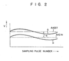
- Fig. 2 is a graphic representation of an output voltage signal derived from an A/
D converter 26, represented as analog signal waveforms; and - Figs. 3A and 3B show flowchart of the discrimination operation carried by the apparatus shown in Fig. 1.
- Fig. 1 shows a block diagram of an apparatus for discriminating a paper-like material according to a preferred embodiment._
- The apparatus shown in Fig. 1 is so designed as to discriminate a
bank note 10. First, thenote 10 is conveyed in the direction of anarrow 14 along,aconvey path 12 at a given convey speed. A part of afront surface 16 of thenote 10 is used as adetection area 30. For the sake of simplicity, a part of this detection area is indicated in the drawing by the hatched area. This area is optically scanned in the conveyingdirection 14 so as to establish theentire detection area 30. Alight source 18, coupled to a power source (not shown), and alight receiver 20 are positioned apart at a given distance from thedetection area 30 of thefront surface 16 of thenote 10. This optical system is arranged in such a manner thatlight rays 21 radiated from thelight source 18 are incident upon thedetection area 30. Thelight receiver 20 receives therays 23 reflected from thedetection area 30. - Secondly, the optical signal of the
light receiver 20 is supplied to a photoelectric converting circuit and converted into a corresponding electric signal. The electric output signal from thephotoelectric converting circuit 24 is applied to an A/D converter 26. An output terminal of the A/D converter 26 is connected to anarithmetic logic unit 28 and also to afirst memory section 32,second memory section 34, athird memory section 36, acounter 38 and afourth memory section 40. - A
central control circuit 42 is provided in the apparatus. The output terminal of thiscircuit 42 is connected to anarithmetic logic unit 28, afirst memory section 32, ansecond memory section 34, athird memory section 36, acounter 38, and afourth memory section 40 so as to supply control signals to them. Further atiming control circuit 44 is provided to control the sampling timing of the A/D converter 26 and to apply its timing control information (sampling pulse signals) to thecentral control circuit 42. - The function of the A/
D converter 26, as is well known, is to convert analog (electric) signals obtained by optically-scanning thedetection area 30 of thenote 10 into digital signals. In the present embodiment, the digital signals are sampled by sampling pulse signals generated in thetiming control circuit 44 and, then, the sampled digital signals are applied to a processing circuit. - The
first memory section 32 used as the main memory is functionally divided into a plurality of sub-regions for storing a standard pattern, an input pattern and data on the arithmetic operation. Thesecond memory section 34 stores a level "E" (a first presettable value) which is used to produce a discrimination pattern, and thethird memory section 36 stores a count "F" (a second presettable value). The arithmetic logic unit 28 (ALU) performs the arithmetic logic operation. Thecounter 38 is resettable and actuated by the ALU 28 and thethird memory section 36. Thecentral control circuit 42 controls the operations of the overall circuit. Thefourth memory section 40 stores a third presettable value "K" which is used for discriminating that almost theentire note 10 is soiled. - It should be noted that the first presettable level "E" must be set to a given value smaller than the maximum value of the output voltage signal derived from the photoelectric converting circuit, and the second presettable count "F" must be set to a given value or number is smaller than all sampling numbers of the A/
D converter 26 with respect to onenote 10. - The operation of the circuit shown in Fig. 1 will be explained with reference to the waveforms of the sampled digital signals derived from the A/D converter 26 (represented as analog signal waveforms for the simplicity) as shown in Fig. 2 and the flow chart in Fig. 3.
- First, a print pattern of a standard bank note (not shown) which is clean is optically scanned by the
light source 18, thelight receiver 20 and thephotoelectric converting circuit 24. Precisely speaking, the print pattern defined by thehatched area 30 is scanned by the above optical means along the conveyingdirection 14..(Therefore, the scanned entire area of the print pattern is identical with thedetection area 30 in this specification.) The output analog signals shown in Fig. 2 by a curve "G" are supplied to the A/D converter 26. Thetiming control circuit 44 may produce e.g., "n" sampling pulses and apply them to the A/D converter 26 while a pattern of one note is being read out. Accordingly, the A/D converter 26 converts the analog signal output from thephotoelectric converting circuit 24 into the corresponding digital signal during generation of the sampling pulse, and the thus converted digital signal is stored as a standard pattern data "PS" in thefirst memory section 32. When storing of the standard pattern data "PS" is completed, in other words, thedetection area 30 of thenote 10 has been optically scanned in a longitudinal direction (conveying direction 14), the stored standard pattern data "Ps" is read from thefirst memory section 32 toALU 28. From data "Ps" the average value (AVEST) is calculated (see Fig. 2). Thereafter the thus obtained average value (AVEST) is again stored in thefirst memory section 32. There is an advantage for this mean value calculation is that there is no essential difference between the output signal level of a standard bank note and that of a note of which thedetection area 30 is slightly soiled. If the background color of a note gradually fades after a long circulation, the level of the output signal for thedetection area 30 derived from thephotoelectric converting circuit 24 is proportionally low. Accordingly, this low output signal level need to be distinguished from the defect signal level. Up to this discrimination step, the production of the standard pattern data and its average value "AVEST" has been completed which implies the preparation of the initial data. The discrimination operation may be carried out in accordance with the flow chart in Fig. 3 based upon the initial data. - First, a
note 10 to be discriminated for defects such as stains is optically scanned by the optical devices, which produce an output analog signal having a level "H" (see Fig. 2). The output analog signal is applied to the A/D converter 26. As easily seen from the waveform chart of Fig. 2, the level "H" of this output signal is lower than the level "G" of the output signal obtained by scanning the standard bank note. This means that thedetection area 30 of thenote 10 is soiled. When the analog signal having the level "H" is converted into a digital signal in the A/D converter 26 in such a manner that the A/D conversion is effected at each timing, the sampling pulse is applied to the A/D converter 26 from thetiming control circuit 44. The resultant digital signal is stored as input pattern data "PI" in thefirst memory section 32. Similarly n sampling pulses for thenote 10 are applied to the A/D converter 26. In other words, A/D conversion is carried out n times. - After the
detection area 30 of thenote 10 is optically and electrically read out, the input pattern data "PI" is read from thefirst memory section 32 and its average value (AVEIN) is calculated byALU 28. - An average value difference (X) in a digital value between this average value (AVEIN) and the previously obtained one (AVEST) for the standard pattern is also calculated by
ALU 28. In thisALU 28, the difference (X) of the average values is used to correct the input pattern data for every sampling pulse, i.e., - Accordingly the input pattern data is shifted up if the difference (X) has a positie value, and is shifted down if the difference (X) has a negative value. In this embodiment the input pattern data "PI" is shifted up since the difference (X) has a positive value (see Fig. 2).
- Before the above-mentioned correction, it is determined whether the
entire detection area 30 of thenote 10 is soiled or not. That is, comparing the difference (X) for correction with a third presettable value (K) which is stored in advance in thefourth memory section 40, a decision is made that thenote 10 is soiled in the. entire region if "K" is greater than or equal to "X" (see flow chart of Fig. 3). - In the next step, the standard pattern data (PS) is read from the
first memory section 32 toALU 28. - In
ALU 28, the corrected input pattern (PI') is subtracted from the standard pattern data (PS) for every sampling pulse so as to obtain a second difference (I). Then the second difference (I) is compared with the first presettable level (E) stored in thesecond memory section 34. Only when "I" is greater than or equal to "E", thecounter 38 counts up by "1". As was previously described, this counter is already initialized to "0". Such a comparison between the second difference (I) and the first presettable value (E) is repeated m times. This number, m, is equal to the number, n. - Preceding the next step, the count (J) of the
counter 38 is compared with the second presettable value (F) stored in thethird memory section 36. If "J" is smaller than "F", thenote 10 has no defect. - If "J" is greater than or equal to "F", it has a defect.
- In accordance with such an apparatus for discriminating defects in paper-like material, it can reliably discriminate defects of any kind in the print patterns without adverse influence from the print patterns themselves. Moreover, the apparatus is very useful because the user can freely preset the degree of the stain, i.e., the first presettable value "E", and also the area of the stain i.e., the second presettable value "F".
- While the present invention has been described using specific embodiments, it should be understood that another modifications and changes can be made without departing from the scope of the present invention.
- Throughout the previous embodiments, two requirements, i.e., the degree and area of the stain, were employed as the discrimination conditions. It is however possible to introduce only one of these requirements as the discrimination condition. In the latter case, the discriminating operation is simplified and requires less time.
- Furthermore, the third presettable value "K" stored in the fourth memory section may be omitted if the entire detection area of the paper-like material is not soiled.
- Although the difference "I" was calculated after the input pattern data "PI" had been corrected by the average value difference "X" and thereafter was compared with the first presettable value "E", the first presettable value "E" can be changed by the average value without average-correcting the input pattern data PI. The counter counted up from "0" in the embodiment. The second presettable value "F" may-be preset in the counter before the discriminating operation, and the counter may count down from the preset value, for example.
Claims (4)
Applications Claiming Priority (2)
| Application Number | Priority Date | Filing Date | Title |
|---|---|---|---|
| JP57166584A JPS5957108A (en) | 1982-09-27 | 1982-09-27 | System for judging damage of paper |
| JP166584/82 | 1982-09-27 |
Publications (3)
| Publication Number | Publication Date |
|---|---|
| EP0109490A2 true EP0109490A2 (en) | 1984-05-30 |
| EP0109490A3 EP0109490A3 (en) | 1986-09-10 |
| EP0109490B1 EP0109490B1 (en) | 1988-08-17 |
Family
ID=15833981
Family Applications (1)
| Application Number | Title | Priority Date | Filing Date |
|---|---|---|---|
| EP83108424A Expired EP0109490B1 (en) | 1982-09-27 | 1983-08-26 | Apparatus for discriminating a paper-like material |
Country Status (4)
| Country | Link |
|---|---|
| US (1) | US4550433A (en) |
| EP (1) | EP0109490B1 (en) |
| JP (1) | JPS5957108A (en) |
| DE (1) | DE3377752D1 (en) |
Cited By (8)
| Publication number | Priority date | Publication date | Assignee | Title |
|---|---|---|---|---|
| FR2601449A1 (en) * | 1986-07-11 | 1988-01-15 | Laurel Bank Machine Co | DEVICE FOR ADJUSTING OPTICAL SENSORS |
| DE3812268A1 (en) * | 1987-04-13 | 1988-11-03 | Laurel Bank Machine Co | ADJUSTABLE TEST DEVICE FOR DETECTING DAMAGED BANKNOTES |
| EP0338123A2 (en) * | 1988-04-18 | 1989-10-25 | Mars Incorporated | Device for verifying documents |
| US5034616A (en) * | 1989-05-01 | 1991-07-23 | Landis & Gyr Betriebs Ag | Device for optically scanning sheet-like documents |
| EP0555873A2 (en) * | 1992-02-14 | 1993-08-18 | Intel Corporation | Method and apparatus for detecting fades in digital video sequences |
| WO1996019781A2 (en) * | 1994-12-21 | 1996-06-27 | Riss Int. S.A. | Document cataloging device |
| EP0982565A2 (en) * | 1998-08-24 | 2000-03-01 | Kabushiki Kaisha Toshiba | Apparatus for examining the degree of stain of printed matter |
| US7672499B2 (en) | 1990-02-05 | 2010-03-02 | Cummins-Allison Corp. | Method and apparatus for currency discrimination and counting |
Families Citing this family (18)
| Publication number | Priority date | Publication date | Assignee | Title |
|---|---|---|---|---|
| GB2164442A (en) * | 1984-09-11 | 1986-03-19 | De La Rue Syst | Sensing the condition of a document |
| US4899392A (en) * | 1987-12-03 | 1990-02-06 | Cing Corporation | Method and system for objectively grading and identifying coins |
| SE458316B (en) * | 1988-02-17 | 1989-03-13 | Inter Innovation Ab | DEVICE FOR CONTROL OF DOCUMENTS |
| JP2531766B2 (en) * | 1988-12-22 | 1996-09-04 | 株式会社東芝 | Shape detection device for paper sheets |
| SG126671A1 (en) * | 1989-02-10 | 2006-11-29 | Canon Kk | Apparatus for image reading or processing |
| US4973851A (en) * | 1989-04-07 | 1990-11-27 | Rowe International, Inc. | Currency validator |
| US5426509A (en) * | 1993-05-20 | 1995-06-20 | Peplinski; Robert A. | Device and method for detecting foreign material on a moving printed film web |
| ITBO940153A1 (en) * | 1994-04-12 | 1995-10-12 | Gd Spa | METHOD FOR OPTICAL CONTROL OF PRODUCTS. |
| US5889883A (en) * | 1995-01-23 | 1999-03-30 | Mars Incorporated | Method and apparatus for optical sensor system and optical interface circuit |
| GB9519886D0 (en) * | 1995-09-29 | 1995-11-29 | At & T Global Inf Solution | Method and apparatus for scanning bank notes |
| US7584883B2 (en) | 1996-11-15 | 2009-09-08 | Diebold, Incorporated | Check cashing automated banking machine |
| US6573983B1 (en) | 1996-11-15 | 2003-06-03 | Diebold, Incorporated | Apparatus and method for processing bank notes and other documents in an automated banking machine |
| US7559460B2 (en) | 1996-11-15 | 2009-07-14 | Diebold Incorporated | Automated banking machine |
| US7513417B2 (en) | 1996-11-15 | 2009-04-07 | Diebold, Incorporated | Automated banking machine |
| US5923413A (en) * | 1996-11-15 | 1999-07-13 | Interbold | Universal bank note denominator and validator |
| GB2332270A (en) * | 1997-12-10 | 1999-06-16 | Mars Inc | Charge storage photoelectric measurement |
| EP1434176A1 (en) * | 2002-12-27 | 2004-06-30 | Mars, Incorporated | Banknote validator |
| US9049904B2 (en) | 2010-02-26 | 2015-06-09 | Ykk Corporation | Button fastener, method for forming button fastener, eyelet, and method for forming eyelet |
Citations (5)
| Publication number | Priority date | Publication date | Assignee | Title |
|---|---|---|---|---|
| US2950799A (en) * | 1952-02-07 | 1960-08-30 | Alan Foster | Apparatus for identifying paper money, or the like, as genuine, and for making change or the like |
| US4197584A (en) * | 1978-10-23 | 1980-04-08 | The Perkin-Elmer Corporation | Optical inspection system for printing flaw detection |
| US4298807A (en) * | 1978-12-01 | 1981-11-03 | Compagnie Industrielle Radioelectrique | Process for inspecting the physical state of a printed document and an installation for putting the process into operation |
| US4311914A (en) * | 1978-12-18 | 1982-01-19 | Gretag Aktiengesellschaft | Process for assessing the quality of a printed product |
| GB2115145A (en) * | 1981-07-29 | 1983-09-01 | Dainippon Printing Co Ltd | Method and device for inspecting printed matter |
Family Cites Families (3)
| Publication number | Priority date | Publication date | Assignee | Title |
|---|---|---|---|---|
| US4041456A (en) * | 1976-07-30 | 1977-08-09 | Ott David M | Method for verifying the denomination of currency |
| AT349248B (en) * | 1976-11-29 | 1979-03-26 | Gao Ges Automation Org | PROCEDURE FOR DYNAMIC MEASUREMENT OF THE DEGREE OF CONTAMINATION OF BANKNOTES AND TESTING DEVICE FOR PERFORMING THIS PROCESS |
| JPS5674790A (en) * | 1979-11-22 | 1981-06-20 | Tokyo Shibaura Electric Co | Bill discriminator |
-
1982
- 1982-09-27 JP JP57166584A patent/JPS5957108A/en active Pending
-
1983
- 1983-08-26 EP EP83108424A patent/EP0109490B1/en not_active Expired
- 1983-08-26 DE DE8383108424T patent/DE3377752D1/en not_active Expired
- 1983-08-31 US US06/528,106 patent/US4550433A/en not_active Expired - Lifetime
Patent Citations (5)
| Publication number | Priority date | Publication date | Assignee | Title |
|---|---|---|---|---|
| US2950799A (en) * | 1952-02-07 | 1960-08-30 | Alan Foster | Apparatus for identifying paper money, or the like, as genuine, and for making change or the like |
| US4197584A (en) * | 1978-10-23 | 1980-04-08 | The Perkin-Elmer Corporation | Optical inspection system for printing flaw detection |
| US4298807A (en) * | 1978-12-01 | 1981-11-03 | Compagnie Industrielle Radioelectrique | Process for inspecting the physical state of a printed document and an installation for putting the process into operation |
| US4311914A (en) * | 1978-12-18 | 1982-01-19 | Gretag Aktiengesellschaft | Process for assessing the quality of a printed product |
| GB2115145A (en) * | 1981-07-29 | 1983-09-01 | Dainippon Printing Co Ltd | Method and device for inspecting printed matter |
Cited By (14)
| Publication number | Priority date | Publication date | Assignee | Title |
|---|---|---|---|---|
| FR2601449A1 (en) * | 1986-07-11 | 1988-01-15 | Laurel Bank Machine Co | DEVICE FOR ADJUSTING OPTICAL SENSORS |
| DE3812268A1 (en) * | 1987-04-13 | 1988-11-03 | Laurel Bank Machine Co | ADJUSTABLE TEST DEVICE FOR DETECTING DAMAGED BANKNOTES |
| US5055834A (en) * | 1987-04-13 | 1991-10-08 | Laurel Bank Machines Co., Ltd. | Adjustable bill-damage discrimination system |
| EP0338123A2 (en) * | 1988-04-18 | 1989-10-25 | Mars Incorporated | Device for verifying documents |
| EP0338123A3 (en) * | 1988-04-18 | 1989-12-20 | Lgz Landis & Gyr Zug Ag | Device for acknowledging documents |
| US5034616A (en) * | 1989-05-01 | 1991-07-23 | Landis & Gyr Betriebs Ag | Device for optically scanning sheet-like documents |
| US7672499B2 (en) | 1990-02-05 | 2010-03-02 | Cummins-Allison Corp. | Method and apparatus for currency discrimination and counting |
| EP0555873A2 (en) * | 1992-02-14 | 1993-08-18 | Intel Corporation | Method and apparatus for detecting fades in digital video sequences |
| EP0555873A3 (en) * | 1992-02-14 | 1994-12-21 | Intel Corp | |
| WO1996019781A2 (en) * | 1994-12-21 | 1996-06-27 | Riss Int. S.A. | Document cataloging device |
| WO1996019781A3 (en) * | 1994-12-21 | 1996-08-22 | Riss Int S A | Document cataloging device |
| EP0982565A2 (en) * | 1998-08-24 | 2000-03-01 | Kabushiki Kaisha Toshiba | Apparatus for examining the degree of stain of printed matter |
| EP0982565A3 (en) * | 1998-08-24 | 2000-06-21 | Kabushiki Kaisha Toshiba | Apparatus for examining the degree of stain of printed matter |
| US6556693B1 (en) | 1998-08-24 | 2003-04-29 | Kabushiki Kaisha Toshiba | Apparatus for examining the degree of stain on printed matter |
Also Published As
| Publication number | Publication date |
|---|---|
| DE3377752D1 (en) | 1988-09-22 |
| JPS5957108A (en) | 1984-04-02 |
| US4550433A (en) | 1985-10-29 |
| EP0109490B1 (en) | 1988-08-17 |
| EP0109490A3 (en) | 1986-09-10 |
Similar Documents
| Publication | Publication Date | Title |
|---|---|---|
| EP0109490A2 (en) | Apparatus for discriminating a paper-like material | |
| EP0069893B1 (en) | A printed matter identifying apparatus and method | |
| US4850029A (en) | Adaptive threshold circuit for image processing | |
| EP0213949B1 (en) | Image processing apparatus | |
| US4234895A (en) | Converting a video signal into a two-level signal | |
| JPH0377475B2 (en) | ||
| US3662341A (en) | Video-derived segmentation-gating apparatus for optical character recognition | |
| US2885551A (en) | Variable voltage level discriminator varying with the input voltage level | |
| US3263216A (en) | Pattern recognition error correction system employing variable parameter input devices | |
| US4740843A (en) | Method and device for recognizing half-tone image information | |
| US4257070A (en) | Method for converting a video signal into a black/white signal | |
| US2943208A (en) | Apparatus for regulating output of photosensitive scanners | |
| GB2082878A (en) | Digital measurement system for automatically focusing a television camera | |
| EP0505970B1 (en) | White level detection circuit for an optical image reader | |
| JPS59176606A (en) | Detector for edge of flat plate body | |
| JPS58106570A (en) | Picture discriminating device | |
| JPS57172365A (en) | Detection method for original density of copying machine | |
| US5253080A (en) | Picture signal binarization apparatus avoiding a need for memory devices or shift registers for storing binary picture signals before output | |
| JPS5888965A (en) | Check system for amount of light | |
| EP0198525B1 (en) | A device for determining a value representative of the amount of weak information of an original | |
| JPS5937763A (en) | Original and original width detector of picture reader | |
| JPS6220093A (en) | Inspecting device for printed character or the like | |
| JPS61229183A (en) | Sheet paper discriminator | |
| JPS62137695A (en) | Sheet paper discriminator | |
| JPS60196068A (en) | Area discriminating method |
Legal Events
| Date | Code | Title | Description |
|---|---|---|---|
| PUAI | Public reference made under article 153(3) epc to a published international application that has entered the european phase |
Free format text: ORIGINAL CODE: 0009012 |
|
| 17P | Request for examination filed |
Effective date: 19830923 |
|
| AK | Designated contracting states |
Designated state(s): DE FR GB IT NL |
|
| RAP1 | Party data changed (applicant data changed or rights of an application transferred) |
Owner name: KABUSHIKI KAISHA TOSHIBA |
|
| PUAL | Search report despatched |
Free format text: ORIGINAL CODE: 0009013 |
|
| AK | Designated contracting states |
Kind code of ref document: A3 Designated state(s): DE FR GB IT NL |
|
| 17Q | First examination report despatched |
Effective date: 19870211 |
|
| GRAA | (expected) grant |
Free format text: ORIGINAL CODE: 0009210 |
|
| AK | Designated contracting states |
Kind code of ref document: B1 Designated state(s): DE FR GB IT NL |
|
| REF | Corresponds to: |
Ref document number: 3377752 Country of ref document: DE Date of ref document: 19880922 |
|
| ITF | It: translation for a ep patent filed |
Owner name: BUGNION S.P.A. |
|
| ET | Fr: translation filed | ||
| PLBI | Opposition filed |
Free format text: ORIGINAL CODE: 0009260 |
|
| 26 | Opposition filed |
Opponent name: GAO GESELLSCHAFT FUER AUTOMATION UND ORGANISATION Effective date: 19890516 |
|
| NLR1 | Nl: opposition has been filed with the epo |
Opponent name: GAO GESELLSCHAFT FUER AUTOMATION UND ORGANISATION |
|
| PGFP | Annual fee paid to national office [announced via postgrant information from national office to epo] |
Ref country code: GB Payment date: 19910805 Year of fee payment: 9 |
|
| PGFP | Annual fee paid to national office [announced via postgrant information from national office to epo] |
Ref country code: FR Payment date: 19910808 Year of fee payment: 9 |
|
| ITTA | It: last paid annual fee | ||
| PGFP | Annual fee paid to national office [announced via postgrant information from national office to epo] |
Ref country code: NL Payment date: 19910831 Year of fee payment: 9 |
|
| PGFP | Annual fee paid to national office [announced via postgrant information from national office to epo] |
Ref country code: DE Payment date: 19910930 Year of fee payment: 9 |
|
| RDAG | Patent revoked |
Free format text: ORIGINAL CODE: 0009271 |
|
| STAA | Information on the status of an ep patent application or granted ep patent |
Free format text: STATUS: PATENT REVOKED |
|
| 27W | Patent revoked |
Effective date: 19920214 |
|
| GBPR | Gb: patent revoked under art. 102 of the ep convention designating the uk as contracting state | ||
| NLR2 | Nl: decision of opposition |