EP0094234A2 - Combinational logic structure using pass transistors - Google Patents
Combinational logic structure using pass transistors Download PDFInfo
- Publication number
- EP0094234A2 EP0094234A2 EP83302602A EP83302602A EP0094234A2 EP 0094234 A2 EP0094234 A2 EP 0094234A2 EP 83302602 A EP83302602 A EP 83302602A EP 83302602 A EP83302602 A EP 83302602A EP 0094234 A2 EP0094234 A2 EP 0094234A2
- Authority
- EP
- European Patent Office
- Prior art keywords
- pass
- variables
- function
- truth table
- state
- Prior art date
- Legal status (The legal status is an assumption and is not a legal conclusion. Google has not performed a legal analysis and makes no representation as to the accuracy of the status listed.)
- Granted
Links
Images


Classifications
-
- G—PHYSICS
- G06—COMPUTING; CALCULATING OR COUNTING
- G06F—ELECTRIC DIGITAL DATA PROCESSING
- G06F7/00—Methods or arrangements for processing data by operating upon the order or content of the data handled
- G06F7/38—Methods or arrangements for performing computations using exclusively denominational number representation, e.g. using binary, ternary, decimal representation
- G06F7/48—Methods or arrangements for performing computations using exclusively denominational number representation, e.g. using binary, ternary, decimal representation using non-contact-making devices, e.g. tube, solid state device; using unspecified devices
- G06F7/50—Adding; Subtracting
- G06F7/501—Half or full adders, i.e. basic adder cells for one denomination
- G06F7/503—Half or full adders, i.e. basic adder cells for one denomination using carry switching, i.e. the incoming carry being connected directly, or only via an inverter, to the carry output under control of a carry propagate signal
-
- G—PHYSICS
- G06—COMPUTING; CALCULATING OR COUNTING
- G06F—ELECTRIC DIGITAL DATA PROCESSING
- G06F7/00—Methods or arrangements for processing data by operating upon the order or content of the data handled
- G06F7/38—Methods or arrangements for performing computations using exclusively denominational number representation, e.g. using binary, ternary, decimal representation
- G06F7/48—Methods or arrangements for performing computations using exclusively denominational number representation, e.g. using binary, ternary, decimal representation using non-contact-making devices, e.g. tube, solid state device; using unspecified devices
- G06F7/50—Adding; Subtracting
-
- H—ELECTRICITY
- H03—ELECTRONIC CIRCUITRY
- H03K—PULSE TECHNIQUE
- H03K19/00—Logic circuits, i.e. having at least two inputs acting on one output; Inverting circuits
- H03K19/02—Logic circuits, i.e. having at least two inputs acting on one output; Inverting circuits using specified components
- H03K19/08—Logic circuits, i.e. having at least two inputs acting on one output; Inverting circuits using specified components using semiconductor devices
- H03K19/094—Logic circuits, i.e. having at least two inputs acting on one output; Inverting circuits using specified components using semiconductor devices using field-effect transistors
- H03K19/0944—Logic circuits, i.e. having at least two inputs acting on one output; Inverting circuits using specified components using semiconductor devices using field-effect transistors using MOSFET or insulated gate field-effect transistors, i.e. IGFET
- H03K19/09441—Logic circuits, i.e. having at least two inputs acting on one output; Inverting circuits using specified components using semiconductor devices using field-effect transistors using MOSFET or insulated gate field-effect transistors, i.e. IGFET of the same canal type
-
- H—ELECTRICITY
- H03—ELECTRONIC CIRCUITRY
- H03K—PULSE TECHNIQUE
- H03K19/00—Logic circuits, i.e. having at least two inputs acting on one output; Inverting circuits
- H03K19/20—Logic circuits, i.e. having at least two inputs acting on one output; Inverting circuits characterised by logic function, e.g. AND, OR, NOR, NOT circuits
- H03K19/21—EXCLUSIVE-OR circuits, i.e. giving output if input signal exists at only one input; COINCIDENCE circuits, i.e. giving output only if all input signals are identical
- H03K19/215—EXCLUSIVE-OR circuits, i.e. giving output if input signal exists at only one input; COINCIDENCE circuits, i.e. giving output only if all input signals are identical using field-effect transistors
-
- H—ELECTRICITY
- H03—ELECTRONIC CIRCUITRY
- H03K—PULSE TECHNIQUE
- H03K23/00—Pulse counters comprising counting chains; Frequency dividers comprising counting chains
-
- H—ELECTRICITY
- H03—ELECTRONIC CIRCUITRY
- H03M—CODING; DECODING; CODE CONVERSION IN GENERAL
- H03M11/00—Coding in connection with keyboards or like devices, i.e. coding of the position of operated keys
- H03M11/02—Details
-
- G—PHYSICS
- G06—COMPUTING; CALCULATING OR COUNTING
- G06F—ELECTRIC DIGITAL DATA PROCESSING
- G06F2207/00—Indexing scheme relating to methods or arrangements for processing data by operating upon the order or content of the data handled
- G06F2207/38—Indexing scheme relating to groups G06F7/38 - G06F7/575
- G06F2207/48—Indexing scheme relating to groups G06F7/48 - G06F7/575
- G06F2207/4802—Special implementations
- G06F2207/4816—Pass transistors
Definitions
- This invention relates to logic circuits and in particular to a logical element known as a PASS transistor and to logic circuits formed using PASS transistors so as to substantially reduce the number of active devices required to implement logic functions.
- Boolean logic expressions may be realized through classical logic design methods with networks of combinational logic. Logic networks using MOS technology are often formed with NAND, NOR and Inversion gates since these structures are easily implemented.
- the PASS transistor is another common MOS structure. See “Introduction to VLSI Systems" by Mead and Conway, pages 24 and 25, for example, for a description of PASS transistors. Classical logic design methods, however, do not result in networks of PASS transistors.
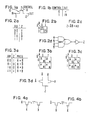
- Figure la shows the PASS transistor with its logical function.
- transistor 10 passes the logic state at input lead 11 to output lead 12.
- the input and output leads of an MOS transistor may be arbitrarily chosen because an MOS transistor is bidirectional.
- the input lead shall hereafter be defined as the terminal driven by the source of a logic state.
- the output lead 12 of PASS transistor 10 typically applies the passed logic state to the input lead of another series connected logic structure.
- Output leads of a number of PASS transistors may be joined to drive the same input of a logic structure provided that all PASS transistors whose controls are asserted are passing the same logic state.
- PASS transistors as bidirectional transmission gates is described in an article entitled "VLSI: A New Frontier for Systems Designers" published in the January 1982 Computer Journal of the IEEE by Douglas G. Fairbairn, which is hereby incorporated by reference.
- logic networks are fabricated using PASS transistors so as to maximize the regularity of the resulting logic circuitry.
- the resulting logical networks give significant topological, power and speed advantages over prior art logic circuits when used to form combinational logic.
- the use of the PASS transistor as a logic element yields several advantages over the NAND, NOR and inverter structures used in prior art logic circuits such as MOS- integrated logic circuits.
- the PASS transistor dissipates no significant steady state power.
- arrays of PASS transistors form structures of regular topology often consuming less area for a given logical function than consumed by NAND, NOR and inverter arrays.
- combinational logic formed with PASS transistors often reduces the signal propagation delay through a network.
- the major disadvantage of the PASS transistor is that the voltage level of the logic high signal on its output lead is degraded due to the characteristics of the field effect transistor used as the PASS transistor, this can be overcome by careful circuit design. However, after passing a logic high level through one PASS transistor, no significant further degradation of voltage level occurs when the signal is passed through N additional PASS transistors assuming no PASS transistor control input is driven by the output of another PASS transistor.
- FIG. 2a shows the truth table for an Exclusive NOR or equivalence gate.
- the truth table information is then entered into a Karnaugh map.
- the output function is reduced and read from the Karnaugh map using looping techniques.
- a Karnaugh map reduction of the Exclusive NOR truth table is shown in Figure 2b, with the Boolean expression shown in Figure 2c.
- the function is then implemented using logic AND function and OR function gates. The implementation of this function with prior art logic structures requires two AND functions and one OR function.
- a possible MOS configuration has two nodes which dissipate power, two gate delays and consists of 7 transistors.
- input variables A and B are both low and the output variable B is high.
- Z may be formed by passing the inversion of A or the inversion of B (i.e. A or B).
- B is high.
- Z is low, 3 may be formed by passing A or the inverse of B (i.e. A or B).
- the PASS functions of the other two states are similarly obtained and shown in the truth table in Figure 3a.
- a "care” state is an input state for which the output state must be defined and is often referred to simply as a "state”.
- PASS function guarantees that the passed variables are the same logic level in a given state.
- a possible mapping for the equivalence gate using PASS transistors is to pass the inverse of B when A is low and to pass B when A is high. This mapping is shown in Figure 3c.
- A is the CONTROL function that passes the PASS function B and A is the CONTROL function that passes the PASS function B.
- the PASS transistor network obtained is shown in Figure 3d.
- the PASS transistor Exclusive NOR shown in Figure 3d dissipates no significant steady state power, has one PASS transistor delay and consists of only two transistors. Thus a substantial power, speed and area savings over the classical logic design methods is realized.
- a "CONTROL” variable is the input variable which drives the control terminal of a PASS transistor.
- a "PASS” variable is the input variable which drives the input terminal of a PASS transistors and which is passed to the output terminal when the PASS transistor is turned on.
- Regularity may be maximized in the CONTROL function if the CONTROL functions can be looped such that they are functions of only the control variables. Regularity in the PASS function may be maximized by making the PASS function independent of the control variables. This independence may be established through the use of the following identities.
- the iterative combinational array is a class of combinational logic for which the area of one circuit configuration versus another may easily be compared. Area may be compared by drawing the layout of one element of the array.
- a useful circuit illustrative of iterative combinational arrays is the digital magnitude comparator.
- the first step in designing the magnitude comparator is to establish a truth table as illustrated in Figure 6.
- the possible passed variables are then added to the truth table to define the PASS functions for each state and these passed variables are entered into a modified Karnaugh map. (In simple cases, where the identical pass variables associated with different states can be identified from the truth table, the modified Karnaugh map can be omitted). Groups of passed variables are then ready to be looped (i.e. identified and circled for ease of reference). Since C i+1 and D i+1 influence directly C i and D i , respectively, these are good choices for passed variables.
- the CONTROL functions are functions of only variables A i and B i and the PASS functions C i+1 and D i+1 are independent of A i and B i .
- the circuit schematic of the PASS transistor array is shown in Figure 8a and the integrated circuit layout in N channel MOS technology is shown in Figure 8b.
- an MOS transistor is depicted by the crossing of two perpendicular lines and a conductive crossunder is depicted by a dark rectangle.
- the gate electrodes are the vertical lines labeled A i , A i , B i and B i and the horizontal lines labeled C i+1 and D i+1 comprise diffused conductive lines and source and drain regions.
- the basic design method for constructing a logic circuit using the PASS transistor as the basic element is as follows:
- FIGS 3a through 3d discussed above, illustrate this procedure. As explained above, in some cases, step 3 can be omitted.
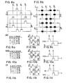
- Figures 9a, 9b and 9c illustrate, respectively, this method for specifying the PASS transistor logic circuit representing an AND gate.
- a PASS transistor logic circuit is implemented using only two PASS transistors as compared to three to five transistors using the prior art implementation.
- Figures 10a, 10b and 10c illustrate, respectively, the truth table, Karnaugh plot and logic circuit implemented using PASS transistors for a NAND gate. Again, the inherent simplicity of the logic circuit utilizing PASS transistors in accordance with this invention is apparent.
- Figures lla, llb and llc illustrate, respectively, the truth table, Karnaugh plot and logic network constructed using PASS transistors of an OR gate.
- the PASS function A has been replaced with the supply voltage V DD in accordance with the identity of Figure 4a.
- Figures 12a, 12b and 12c illustrate, respectively, the truth table, Karnaugh plot and logic circuitry of a NOR gate constructed using PASS transistors.
- the PASS function A has been replaced with the reference voltage V SS in accordance with the identity of Figure 4b.
- Figures 13a, 13b and 13c illustrate, respectively, the truth table, Karnaugh plot and logic circuit constructed using PASS transistors of an exclusive OR gate.
- Figures 14a, 14b and 14c illustrate, respectively, the truth table, Karnaugh plot and logic circuit constructed using PASS transistors of an exclusive NOR gate.
- Each of the structures shown in Figures 9c, 10c, llc, 12c, 13c and 14c uses only two PASS transistors. Each PASS transistor is controlled either by the A or A signal. Each of the logic circuits is capable of producing an appropriate output state in response to any one of the four different possible input states of the two input variables A, B. In Figures 9c, lOc, llc and 12c, none of the PASS variables are related to the CONTROL variables as a result of use of the identities of Figures 4a and 4b. The result is an inherent simplicity in each of the circuits.
- Figures 15a, 15b, 15c and 15d illustrate the implementation of a full adder using the methodology and rules of this invention.
- the carry associated with the full adder (Figure 15d) can be implemented using eight (8) PASS transistors as opposed to a much more complex implementation using standard prior art logic components as illustrated, for example, in Figure 7-3 on page 123 of "Introduction to the Basic Computer” by Donald Eadie, published in 1968 by Prentice-Hall, Inc., Inglewood Cliffs, New Jersey, which is hereby incorporated by reference.
- the sum circuit is formed using another eight (8) PASS transistors and is shown in Figure 16a, 16b and 16c which illustrate the truth table, Karnaugh plot, and PASS transistor implementation, respectively, of a summing network.
- Figure 16d illustrates the layout of the implementation of the circuitry shown in Figure 16c in terms of PASS transistors.
- the regularity and orthogonality of the CONTROL functions and PASS functions is readily apparent from this description.
- the structure is implemented using N channel MOS transistors and the different component layers are indicated as shown by the key associated with the Figure.
- the polysilicon (denoted as "poly") comprises the gate electrodes of the N channel MOS transistors and the diffusion comprises the source and drain regions of these transistors as well as the conductive interconnects between the source and drain regions of adjacent transistors.
- Figure 16d which shows the carry portion of a full adder 15d, the sum network 16c and a complementary carry portion of a full adder derived from the full adder of 15d
- the structure 16d is laid out using N+ diffusions (denoted by the line with an X) polycrystalline silicon (denoted by the straight line) and metal (denoted by the straight line with a cross mark).
- N+ diffusions denoted by the line with an X
- polycrystalline silicon denoted by the straight line
- metal dedenoted by the straight line with a cross mark
- Deep depletion buried cross unders are denoted as dark rectangles.
- the buried cross unders serve as conductive paths for current.
- the MOS transistor is denoted schematically as shown in Figure 16f wherein the polysilicon gate line is orthogonal to an N+ diffusion line.
- Figure 16d represents one portion of an 8-bit adding circuitry and is designed to mate topologically with adjacent portions of the circuitry as shown in Figure 16f.
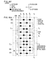
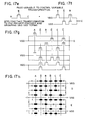
- Figures 17a and 17b illustrate the truth table and the modified Karnaugh map for a priority encoder.
- FIG. 17b A similar analysis for the output variable E is shown in the second part of the modified Karnaugh map of Figure 17b.
- the particular logic shown is implemented in circuit form as shown in Figure 17c and has a layout as shown in Figure 17d.
- the layout of Figure 17d is keyed identically to that of Figure 16d.
- the key to the layout in Figure 16d applies equally to that in Figure 17d and to the other drawings such as shown in Figures 8b, 17h and 19f in this specification.
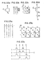
- the PASS variables can then be transformed as shown in Figure 17e and 17f to simplify the structure shown in Figure 17d to form the circuit shown in Figure 17g.
- the circuit in Figure 17g is substantially simpler in terms of topological layout although it contains 16 transistors to the 10 shown in Figure 17c.
- the 16 transistors shown in Figure 17g allow a more rational arrangement of the voltage power lines VDD, VSS and the signal input lines A, A, B, B and C, C.
- Figure 17h illustrates schematically the actual layout of the PASS transistors shown in Figure 17g.
- the comparison between Figure 17c illustrates the type of trade-offs available using the logic system described herein.
- Figure 18a illustrates the schematic block diagram of a binary up/down counter.
- the truth table for this counter is illustrated in Figure 18b.
- Input variables D, T i-1 and Q i control the state of the output variables D i and T i .
- the modified Karnaugh map for output variable D i is shown in Figure 18c and for output variable T i is shown in Figure 18d.
- the output variable T i is generated by the looped PASS functions as illustrated in Figure 18d.
- This structure is shown as implemented in the top two lines of the circuit of Figure 18e.
- the T i output variable is generated by four paths of functions reflecting the four different possible sets of CONTROL functions and PASS functions necessary to generate all possible combinations of T i output signals.
- the T i-1 input signal is passed by the transistors 184 and 185 controlled by the Q i CONTROL signal and the D CONTROL signal, respectively, and for DT i-1 equals 00 or 01 and Q i equals 1, by transistors 182 and 183 controlled by the Q i input signal and the D input signal, respectively.
- Figure 19a illustrates in schematic block diagram form the input and output signals to and from a binary up counter.
- Figure 19b gives the truth table for the input variables T i-1 and Q i and their relationship to the output variables D i and T i .
- Figures 19c and 19d give the modified Karnaugh plots for the output variables D i and T i , respectively, as a function of the input variables T i-1 and Q i .
- Figure 19e illustrates the circuit implementation of the logic using the PASS transistors of this invention derived using the input variables T i-1 and Q i wherein Q i as shown in Karnaugh plot 19d has only the value VSS per the equivalent circuit of Figure 4b.
- Figure 19f illustrates the layout schematically of the circuit shown in Figure 19e.
- Figure 20a gives the truth table for a JK flip-flop with inputs JK and Q and output D.
- Figure 20b shows the modified Karnaugh map for the truth table of Figure 20a.
- Figure 20c shows the circuit implementation of the flip-flop using the PASS functions of this invention. Note that the circuit implementation requires only two PASS transistors reflecting only two looped PASS functions in the modified Karnaugh plot of Figure 20b.
- Figure 20d shows schematically the extremely simple implementation of this structure using again the key shown in Figure 16d.
- Figure 21a illustrates a schematic block diagram of a shift left/hold circuit and the input and output variables to this circuit.
- the input variable C, Q i-1 and Q i produce an output variable D i .
- the modified Karnaugh plot for this circuit is illustrated in Figure 2lc and is implemented as shown in Figure 21d by a two-transistor circuit.
- the schematic layout of this two-transistor circuit is illustrated in Figure 21e.
- the structures of this invention are, as seen from the last two implementations in particular, extremely simple compared to prior art logic implementations.
- the topological advantages of this invention are achieved together with significant reductions in the complexity of components.
- Structures made in accordance with this invention have increased packing density in terms of logic function per unit area and thus possess either smaller size with commensurate increased yield or a substantially larger number of devices formed on a chip of silicon material.
- the devices described above are to be implemented in standard semiconductor processing technology such as N channel MOS technology.
- the invention is capable of being implemented in other semiconductor technologies including P channel MOS technology and CMOS technologies.
- the design of a dynamic D latch is another example of the use of the PASS transistor high impedance state.
- the function of a D latch is to store one bit of information. The information is updated to the logic level of the data input when the load signal LD is asserted high, as shown by the truth table of Figure 22b.
- the data is stored in the form of charge on the gate capacitance of a buffer amplifier 19 ( Figure 22d), when the load signal LD is low.
- the PASS variables are entered into the appropriate states of the Karnaugh map in Figure 22c with X's assigned to the states where charge storage takes place. The map is reduced by grouping the PASS variables in the states without X's. Thus no variable is passed in the charge storage state.
- the resulting PASS network with buffers is shown in the schematic diagram of Figure 22d.
- FIG. 23a-23c show the derivation of a combinational PASS network in accordance with one embodiment of this invention.
- the three variable truth table of Figure 23a is decomposed into two truth tables ( Figure 24a) each having two variables.
- the truth table of Figure 23a is decomposed about the variable A into the two truth tables of Figure 24a.
- the Karnaugh maps of Figure 24b are reduced to form the functions X and Y as depicted in Figure 24c.
- the two circuits providing output signals X and Y of Figure 24c are then joined to form the circuit of Figure 24d providing output signal Z by passing X when A is low and passing Y when A is high.
- the resulting circuit of Figure 24d shows a reduction from 8 transistors (Figure 23c) to 6 transistors ( Figure 24d) to implement the three variable function illustrated in the truth table of Figure 23a.
Abstract
Description
- This invention relates to logic circuits and in particular to a logical element known as a PASS transistor and to logic circuits formed using PASS transistors so as to substantially reduce the number of active devices required to implement logic functions.
- Boolean logic expressions may be realized through classical logic design methods with networks of combinational logic. Logic networks using MOS technology are often formed with NAND, NOR and Inversion gates since these structures are easily implemented. The PASS transistor is another common MOS structure. See "Introduction to VLSI Systems" by Mead and Conway, pages 24 and 25, for example, for a description of PASS transistors. Classical logic design methods, however, do not result in networks of PASS transistors.
- Figure la shows the PASS transistor with its logical function. When the gate or
control electrode 13 toPASS transistor 10 is asserted (and by "asserted" is meant driven to a voltage so as to form a conductive path betweeninput lead 11 and output lead 12),transistor 10 passes the logic state atinput lead 11 tooutput lead 12. The input and output leads of an MOS transistor may be arbitrarily chosen because an MOS transistor is bidirectional. For convenience, the input lead shall hereafter be defined as the terminal driven by the source of a logic state. Theoutput lead 12 ofPASS transistor 10 typically applies the passed logic state to the input lead of another series connected logic structure. Output leads of a number of PASS transistors may be joined to drive the same input of a logic structure provided that all PASS transistors whose controls are asserted are passing the same logic state. The use of PASS transistors as bidirectional transmission gates is described in an article entitled "VLSI: A New Frontier for Systems Designers" published in the January 1982 Computer Journal of the IEEE by Douglas G. Fairbairn, which is hereby incorporated by reference. - In accordance with this invention, logic networks are fabricated using PASS transistors so as to maximize the regularity of the resulting logic circuitry. The resulting logical networks give significant topological, power and speed advantages over prior art logic circuits when used to form combinational logic.
- The use of the PASS transistor as a logic element yields several advantages over the NAND, NOR and inverter structures used in prior art logic circuits such as MOS- integrated logic circuits. First, the PASS transistor dissipates no significant steady state power. Second, arrays of PASS transistors form structures of regular topology often consuming less area for a given logical function than consumed by NAND, NOR and inverter arrays. Third, combinational logic formed with PASS transistors often reduces the signal propagation delay through a network.
- While the major disadvantage of the PASS transistor is that the voltage level of the logic high signal on its output lead is degraded due to the characteristics of the field effect transistor used as the PASS transistor, this can be overcome by careful circuit design. However, after passing a logic high level through one PASS transistor, no significant further degradation of voltage level occurs when the signal is passed through N additional PASS transistors assuming no PASS transistor control input is driven by the output of another PASS transistor.
-
- Figures la and lb illustrate a PASS transistor and the truth table for that transistor;
- Figures 2a through 2d illustrate the logical function Z=AE+AB implemented using AND gates, a NOR gate and an inverter, and the truth table, Karnaugh plot and Boolean equation associated with that structure;
- Figures 3a through 3d illustrate the truth table, the Karnaugh map, the looping of the PASS functions for an equivalence gate and the resulting PASS transistor network, respectively, for the same logical function shown in Figure 2c;
- Figures 4a and 4b illustrate two functional identities which are employed to make logic networks using PASS transistors;
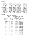
- Figure 5 illustrates in schematic block diagram form a magnitude comparator structure of well known design;
- Figure 6 illustrates the truth table for the magnitude comparator shown in Figure 5;
- Figure 7 illustrates the Karnaugh map and the looping of the PASS functions necessary to produce the logical functions required by the truth table of Figure 6;
- Figures 8a and 8b illustrate the PASS transistor implementation of the logic circuit necessary to implement the truth table of Figure 6 and the silicon layout (in accordance with the conventions shown in Figures 16d and 16f) of the transistors shown in Figure 8a, respectively;
- Figures 9a, 9b and 9c illustrate, respectively, the truth table, Karnaugh map with PASS variables looped and circuit diagram of the resulting logical network for an AND gate;
- Figures 10a, 10b and 10c illustrate, respectively, the truth table, Karnaugh map with PASS functions looped and the logic circuit implemented using PASS transistors for a NAND gate;
- Figures lla, llb and llc illustrate, respectively, the truth table, Karnaugh map with PASS functions looped and the logic circuit implemented using PASS transistors for an OR gate;
- Figures 12a, 12b and 12c illustrate, respectively, the truth table, Karnaugh map with PASS functions looped and the logic circuit implemented using PASS transistors for a NOR gate;
- Figures 13a, 13b and 13c illustrate, respectively, the truth table, Karnaugh map with PASS functions looped and the logic circuit implemented using PASS transistors for an Exclusive OR gate;
- Figures 14a, 14b and 14c illustrate, respectively, the truth table, Karnaugh map with PASS functions looped and the logic circuit implemented using PASS transistors for an Exclusive NOR gate;
- Figures 15a, 15b, 15c and 15d illustrate, respectively, the block diagram, the truth table, the Karnaugh map with PASS functions looped and the logic circuit implementation using PASS transistors, respectively, for the carry generator of a full adder;
- Figures 16a, 16b and 16c illustrate, respectively, the truth table, Karnaugh map with PASS functions looped and the logic circuit implemented using PASS transistors for a summing network of a full adder;
- Figure 16d illustrates the layout of the circuit shown in Figure 16c for the full adder structure;
- Figure 16e illustrates the relationship of the structure of Figure 16d to a complete adding circuit;
- Figure 16f illustrates the way in which an MOS transistor is illustrated in Figure 16d;
- Figures 17a, 17b, 17c and 17d (wherein the components of Figure 17d are labelled in accordance with the conventions of Figures 16d and 16f) illustrate the truth table, the Karnaugh map with the PASS functions circled, the logic circuit implementation using PASS transistors, and the schematic top view of the semiconductor N channel MOS transistor implementation of the circuit of Figure 17c, respectively;
- Figures 17e and 17f illustrate the PASS variable to CONTROL variable transformations used in implementing the structure of Figure 17c;
- Figures 17g and 17h (wherein the components of Figure 17h are labelled in accordance with the conventions of Figures 16d and 16f) illustrate the logic circuitry and the layout of this logic circuitry in N channel MOS technology after the transformations illustrated in Figures 17e and 17f have been applied to the circuit of Figure 17c;
- Figure 18a illustrates a block diagram for a binary up/down counter;
- Figures 18b, 18c, 18d and 18e illustrate, respectively, the truth table, the Karnaugh map with the input PASS functions looped and the circuit implementation of the Karnaugh map;
- Figure 19a illustrates in schematic block form a binary up counter;
- Figures 19b, 19c, 19d, 19e and 19f illustrate, respectively, the truth table, the Karnaugh map with PASS functions looped, the circuit implementation and the N channel MOS transistor implementation for the binary up counter of Figure 19a;
- Figures 20a, 20b, 20c and 20d illustrate, respectively, the truth table, the Karnaugh map with PASS functions looped, the circuit implementation and the N channel MOS transistor implementation for a JK flip-flop;
- Figure 21a illustrates in schematic block diagram form a shift left/hold circuit;
- Figures 21b, 21c, 21d and 21e illustrate, respectively, the truth table, the Karnaugh map with PASS functions circled, the circuit implementation and the N channel MOS transistor implementation of the shift left/hold structure;
- Figures 22a and 22b illustrate, respectively, the schematic block diagram and the truth table of a dynamic D latch;
- Figures 22c and 22d illustrate, respectively, the Karnaugh map and the pass transistor network for the dynamic D latch of Figure 22a;
- Figures 23a, 23b, and 23c illustrate one implementation of a combinational network in accordance with this invention; and
- Figures 24a through 24d illustrate another implementation of the combinational network of Figures 23a-23c in accordance with another embodiment of this invention.
- The classical design of combinational digital logic circuits may be illustrated by the following example. First a truth table for the desired logical function is formed. Figure 2a shows the truth table for an Exclusive NOR or equivalence gate. When input A is equal in value to input B, the output assumes a logic one state. When input A is not equal in value to input B, the output assumes a logic zero state. The truth table information is then entered into a Karnaugh map. The output function is reduced and read from the Karnaugh map using looping techniques. A Karnaugh map reduction of the Exclusive NOR truth table is shown in Figure 2b, with the Boolean expression shown in Figure 2c. The function is then implemented using logic AND function and OR function gates. The implementation of this function with prior art logic structures requires two AND functions and one OR function. A possible MOS configuration has two nodes which dissipate power, two gate delays and consists of 7 transistors.
- The technique for designing combinational logic which results in networks of PASS transistors will now be illustrated. The truth table in Figure 3a shows that the output function 3=AB+AB may be obtained by passing the input variables and/or their inversions. For example, in the first state of the truth table, input variables A and B are both low and the output variable B is high. Thus Z may be formed by passing the inversion of A or the inversion of B (i.e. A or B). In the second state A is low and B is high. Since Z is low, 3 may be formed by passing A or the inverse of B (i.e. A or B). The PASS functions of the other two states are similarly obtained and shown in the truth table in Figure 3a. These PASS functions are then entered into the appropriate states of a Karnaugh map as illustrated in Figure 3b. Note that the PASS formations replace the output signals in a normal Karnaugh map. Identical passed variables are identified in adjacent states on the Karnaugh map and then looped together as shown in Figure 3c to reduce the CONTROL functions. These loopings may use normal Karnaugh map reduction techniques with the following rules. First, a variable must be passed in every "care" state of the map, since the output signal from a PASS transistor is undefined when its control input is low. (A "care" state is an input state for which the output state must be defined and is often referred to simply as a "state".) Second, more than one variable may be passed in each state, since the PASS function guarantees that the passed variables are the same logic level in a given state. Third, once a don't care state has been included in a loop, the pass function is established for that state.
- A possible mapping for the equivalence gate using PASS transistors is to pass the inverse of B when A is low and to pass B when A is high. This mapping is shown in Figure 3c. A is the CONTROL function that passes the PASS function B and A is the CONTROL function that passes the PASS function B. The PASS transistor network obtained is shown in Figure 3d.
- The PASS transistor Exclusive NOR shown in Figure 3d dissipates no significant steady state power, has one PASS transistor delay and consists of only two transistors. Thus a substantial power, speed and area savings over the classical logic design methods is realized.
- The area advantage of one circuit configuration over another is not always obvious from the logic or schematic diagrams. Also a lower transistor count does not guarantee that less silicon area will be used to lay out a circuit since electrical interconnect area requirements are not represented by transistor count. Both transistor count and regularity must be considered when comparing two circuit configurations for area advantages. Network regularity is a concept described, for example, in Chapter 3.1 of "Introduction to VLSI Systems" by Carver Mead and Lynn Conway published by Addison Wesley Publishers, 1980.
- Maximum topological regularity for an array of PASS transistors is established if the intersection of the set of control variables with the set of passed variables is the null set. This allows passed variables to flow in one direction while the control variables flow at right angles. (A "CONTROL" variable is the input variable which drives the control terminal of a PASS transistor. A "PASS" variable is the input variable which drives the input terminal of a PASS transistors and which is passed to the output terminal when the PASS transistor is turned on.) Regularity may be maximized in the CONTROL function if the CONTROL functions can be looped such that they are functions of only the control variables. Regularity in the PASS function may be maximized by making the PASS function independent of the control variables. This independence may be established through the use of the following identities. A PASS transistor whose input is variable X and whose control is also X always passes a one. This is equivalent to a PASS transistor whose input is high and whose control is X as shown in Figure 4a. Similarly, a PASS transistor whose input is X and whose control is X always passes a zero. This is equivalent to a PASS transistor whose input is low and which is controlled by X. Figures 4a and 4b summarize these equivalences.
- The iterative combinational array is a class of combinational logic for which the area of one circuit configuration versus another may easily be compared. Area may be compared by drawing the layout of one element of the array.
- A useful circuit illustrative of iterative combinational arrays is the digital magnitude comparator. The magnitude comparison of two digital words A = An-1, An-2 ...Ai...Ao and B = Bn-1, Bn-2...B1...Bo is accomplished by comparing the ith bits and the results of all more significant bit comparisons. A comparison must produce three pieces of information to be complete: A>B, A = B and A<B, but any one may be derived from the other two. It may be shown that A>B and A<B are good choices to implement. Figure 5 shows the configuration of the comparison where Ci is high indicating AϑBif (Ai>Bi and either Ci+1 = 0, or if Ci+1 = 1) and Di is high indicating A□B if either (Di+1 = 1) or (Ai<Bi and Di+1 = 0).
- The first step in designing the magnitude comparator is to establish a truth table as illustrated in Figure 6. The possible passed variables are then added to the truth table to define the PASS functions for each state and these passed variables are entered into a modified Karnaugh map. (In simple cases, where the identical pass variables associated with different states can be identified from the truth table, the modified Karnaugh map can be omitted). Groups of passed variables are then ready to be looped (i.e. identified and circled for ease of reference). Since Ci+1 and Di+1 influence directly Ci and Di, respectively, these are good choices for passed variables. If the Karnaugh map is looped as shown in Figure 7, the CONTROL functions are functions of only variables Ai and Bi and the PASS functions Ci+1 and Di+1 are independent of Ai and Bi. The circuit schematic of the PASS transistor array is shown in Figure 8a and the integrated circuit layout in N channel MOS technology is shown in Figure 8b. In Figure 8b, an MOS transistor is depicted by the crossing of two perpendicular lines and a conductive crossunder is depicted by a dark rectangle. The gate electrodes are the vertical lines labeled Ai, Ai, Bi and Bi and the horizontal lines labeled Ci+1 and Di+1 comprise diffused conductive lines and source and drain regions.
- The basic design method for constructing a logic circuit using the PASS transistor as the basic element is as follows:
- 1. Establish a truth table of the desired function.
- 2. Enter the PASS function into the truth table (the PASS function is an input variable or its inverse which is passed to the output lead of the PASS transistor to yield the desired output signal).
- 3. Enter the PASS function into a modified Karnaugh map wherein each state of the modified Karnaugh map contains the particular input variables (called the PASS function) which yield the desired output variable.
- 4. Loop (i.e. identify or group) the identical PASS variables in each PASS FUNCTION such that every care state (a care state is one combination of input variables where the output variable must be defined) has at least one PASS variable looped and such that the CONTROL function (i.e., the function that controls the gate of the PASS transistor) is independent of the PASS variables.
- 5. Use the identities shown in Figures 4a and 4b to make the PASS function independent of CONTROL variables.
- 6. Draw the PASS transistor network.
- Figures 3a through 3d, discussed above, illustrate this procedure. As explained above, in some cases, step 3 can be omitted.
- Figures 9a, 9b and 9c illustrate, respectively, this method for specifying the PASS transistor logic circuit representing an AND gate. As shown in Figure 9c, a PASS transistor logic circuit is implemented using only two PASS transistors as compared to three to five transistors using the prior art implementation.
- Note that in the logic circuit of Figure 9c, the PASS function A is replaced with VSS (the circuit ground or reference voltage) in accordance with the identity of Figure 4b.
- Figures 10a, 10b and 10c illustrate, respectively, the truth table, Karnaugh plot and logic circuit implemented using PASS transistors for a NAND gate. Again, the inherent simplicity of the logic circuit utilizing PASS transistors in accordance with this invention is apparent.
- Note that in the logic circuit of Figure 10c, the PASS function A is replaced with VDD (the supply voltage) in accordance with the identity of Figure 4a.
- Figures lla, llb and llc illustrate, respectively, the truth table, Karnaugh plot and logic network constructed using PASS transistors of an OR gate. In the logic circuit of Figure llc, the PASS function A has been replaced with the supply voltage VDD in accordance with the identity of Figure 4a.
- Figures 12a, 12b and 12c illustrate, respectively, the truth table, Karnaugh plot and logic circuitry of a NOR gate constructed using PASS transistors. In the logic circuit of Figure 12c, the PASS function A has been replaced with the reference voltage VSS in accordance with the identity of Figure 4b.
- Figures 13a, 13b and 13c illustrate, respectively, the truth table, Karnaugh plot and logic circuit constructed using PASS transistors of an exclusive OR gate.
- Figures 14a, 14b and 14c illustrate, respectively, the truth table, Karnaugh plot and logic circuit constructed using PASS transistors of an exclusive NOR gate.
- Each of the structures shown in Figures 9c, 10c, llc, 12c, 13c and 14c uses only two PASS transistors. Each PASS transistor is controlled either by the A or A signal. Each of the logic circuits is capable of producing an appropriate output state in response to any one of the four different possible input states of the two input variables A, B. In Figures 9c, lOc, llc and 12c, none of the PASS variables are related to the CONTROL variables as a result of use of the identities of Figures 4a and 4b. The result is an inherent simplicity in each of the circuits.
- Figures 15a, 15b, 15c and 15d illustrate the implementation of a full adder using the methodology and rules of this invention. The carry associated with the full adder (Figure 15d) can be implemented using eight (8) PASS transistors as opposed to a much more complex implementation using standard prior art logic components as illustrated, for example, in Figure 7-3 on page 123 of "Introduction to the Basic Computer" by Donald Eadie, published in 1968 by Prentice-Hall, Inc., Inglewood Cliffs, New Jersey, which is hereby incorporated by reference. The sum circuit is formed using another eight (8) PASS transistors and is shown in Figure 16a, 16b and 16c which illustrate the truth table, Karnaugh plot, and PASS transistor implementation, respectively, of a summing network.
- Figure 16d illustrates the layout of the implementation of the circuitry shown in Figure 16c in terms of PASS transistors. The regularity and orthogonality of the CONTROL functions and PASS functions is readily apparent from this description. The structure is implemented using N channel MOS transistors and the different component layers are indicated as shown by the key associated with the Figure. The polysilicon (denoted as "poly") comprises the gate electrodes of the N channel MOS transistors and the diffusion comprises the source and drain regions of these transistors as well as the conductive interconnects between the source and drain regions of adjacent transistors.
- Thus, in Figure 16d, which shows the carry portion of a
full adder 15d, thesum network 16c and a complementary carry portion of a full adder derived from the full adder of 15d, the structure 16d is laid out using N+ diffusions (denoted by the line with an X) polycrystalline silicon (denoted by the straight line) and metal (denoted by the straight line with a cross mark). Deep depletion buried cross unders are denoted as dark rectangles. The buried cross unders serve as conductive paths for current. The MOS transistor is denoted schematically as shown in Figure 16f wherein the polysilicon gate line is orthogonal to an N+ diffusion line. Underneath the polycrystalline silicon gate in an N+ transistor is a channel region, the conductivity of which is controlled by the signal level on the polycrystalline silicon line. The orthogonality of the layout is apparent from Figure 16d. Figure 16d represents one portion of an 8-bit adding circuitry and is designed to mate topologically with adjacent portions of the circuitry as shown in Figure 16f. - The conventions described above as applicable to Figure 16d apply equally to Figures 8b, 17d, 17h and 19f.
- Figures 17a and 17b illustrate the truth table and the modified Karnaugh map for a priority encoder. The modified Karnaugh map in Figure 17b is in two parts. One part illustrates the particular PASS functions which can be used to obtain the output D. However, the mapping illustrates that for the input variables AB having the
values - A similar analysis for the output variable E is shown in the second part of the modified Karnaugh map of Figure 17b. The particular logic shown is implemented in circuit form as shown in Figure 17c and has a layout as shown in Figure 17d. The layout of Figure 17d is keyed identically to that of Figure 16d. The key to the layout in Figure 16d applies equally to that in Figure 17d and to the other drawings such as shown in Figures 8b, 17h and 19f in this specification.
- The PASS variables can then be transformed as shown in Figure 17e and 17f to simplify the structure shown in Figure 17d to form the circuit shown in Figure 17g. The circuit in Figure 17g is substantially simpler in terms of topological layout although it contains 16 transistors to the 10 shown in Figure 17c. The 16 transistors shown in Figure 17g, however, allow a more rational arrangement of the voltage power lines VDD, VSS and the signal input lines A, A, B, B and C, C. Figure 17h illustrates schematically the actual layout of the PASS transistors shown in Figure 17g. The comparison between Figure 17c illustrates the type of trade-offs available using the logic system described herein.
- Figure 18a illustrates the schematic block diagram of a binary up/down counter. The truth table for this counter is illustrated in Figure 18b. Input variables D, Ti-1 and Qi control the state of the output variables Di and Ti. The modified Karnaugh map for output variable Di is shown in Figure 18c and for output variable Ti is shown in Figure 18d. The particular variables looped to provide the PASS function for generating the output variable Di are shown to be the variable T for Qi = 0 and all values of the variables D and Ti-1, and the variable T for Qi = 1 and all values of D and Ti-1. The output variable Ti is generated by the looped PASS functions as illustrated in Figure 18d. The structure to implement the truth table is as shown in Figure 18e. Note that for all values of the variables D and Ti-1 and for Qi=0, the output function Di is generated by passing the T input signal with the Q control signal. The output variable Di for Q = 1 and all values of D and Ti-1 is generated by passing the input signal T with the Q gate control signal. This structure is shown as implemented in the top two lines of the circuit of Figure 18e. The Ti output variable is generated by four paths of functions reflecting the four different possible sets of CONTROL functions and PASS functions necessary to generate all possible combinations of Ti output signals. For values of DTi-1 equals 11 or 10 and Qi equal 0, the Ti-1 input signal is passed by the
transistors transistors transistors transistors Q i = 1 orQ i = VSS. - Figure 19a illustrates in schematic block diagram form the input and output signals to and from a binary up counter.
- Figure 19b gives the truth table for the input variables Ti-1 and Qi and their relationship to the output variables Di and Ti. Figures 19c and 19d give the modified Karnaugh plots for the output variables Di and Ti, respectively, as a function of the input variables Ti-1 and Qi.
- Figure 19e illustrates the circuit implementation of the logic using the PASS transistors of this invention derived using the input variables Ti-1 and Qi wherein Qi as shown in Karnaugh plot 19d has only the value VSS per the equivalent circuit of Figure 4b.
- Figure 19f illustrates the layout schematically of the circuit shown in Figure 19e.
- Figure 20a gives the truth table for a JK flip-flop with inputs JK and Q and output D.
- Figure 20b shows the modified Karnaugh map for the truth table of Figure 20a.
- Figure 20c shows the circuit implementation of the flip-flop using the PASS functions of this invention. Note that the circuit implementation requires only two PASS transistors reflecting only two looped PASS functions in the modified Karnaugh plot of Figure 20b.
- Figure 20d shows schematically the extremely simple implementation of this structure using again the key shown in Figure 16d.
- Figure 21a illustrates a schematic block diagram of a shift left/hold circuit and the input and output variables to this circuit. The input variable C, Qi-1 and Qi produce an output variable Di. The modified Karnaugh plot for this circuit is illustrated in Figure 2lc and is implemented as shown in Figure 21d by a two-transistor circuit. The schematic layout of this two-transistor circuit is illustrated in Figure 21e.
- The structures of this invention are, as seen from the last two implementations in particular, extremely simple compared to prior art logic implementations. Thus, the topological advantages of this invention are achieved together with significant reductions in the complexity of components. Structures made in accordance with this invention have increased packing density in terms of logic function per unit area and thus possess either smaller size with commensurate increased yield or a substantially larger number of devices formed on a chip of silicon material. Naturally, the devices described above are to be implemented in standard semiconductor processing technology such as N channel MOS technology. The invention, however, is capable of being implemented in other semiconductor technologies including P channel MOS technology and CMOS technologies.
- The design of a dynamic D latch, shown symbolically in Figure 22a, is another example of the use of the PASS transistor high impedance state. The function of a D latch is to store one bit of information. The information is updated to the logic level of the data input when the load signal LD is asserted high, as shown by the truth table of Figure 22b. The data is stored in the form of charge on the gate capacitance of a buffer amplifier 19 (Figure 22d), when the load signal LD is low. The PASS variables are entered into the appropriate states of the Karnaugh map in Figure 22c with X's assigned to the states where charge storage takes place. The map is reduced by grouping the PASS variables in the states without X's. Thus no variable is passed in the charge storage state. The resulting PASS network with buffers is shown in the schematic diagram of Figure 22d.
- The tri-state ability of PASS transistors also allows combinational networks to be simplified by decomposing an N variable map into a plurality of M maps, each having two variables, where 2M-1≤N≤2M. Figures 23a-23c show the derivation of a combinational PASS network in accordance with one embodiment of this invention. In accordance with another embodiment of this invention, the three variable truth table of Figure 23a is decomposed into two truth tables (Figure 24a) each having two variables. The truth table of Figure 23a is decomposed about the variable A into the two truth tables of Figure 24a. The Karnaugh maps of Figure 24b are reduced to form the functions X and Y as depicted in Figure 24c. The two circuits providing output signals X and Y of Figure 24c are then joined to form the circuit of Figure 24d providing output signal Z by passing X when A is low and passing Y when A is high. The resulting circuit of Figure 24d shows a reduction from 8 transistors (Figure 23c) to 6 transistors (Figure 24d) to implement the three variable function illustrated in the truth table of Figure 23a.
- While several embodiments of this invention have been described above, other embodiments of this invention will be obvious in view of the above description to those skilled in the logic design arts. The above description is therefore intended to be illustrative only and not limiting.
Claims (6)
drawing the PASS transistor network.
Priority Applications (1)
| Application Number | Priority Date | Filing Date | Title |
|---|---|---|---|
| AT83302602T ATE41276T1 (en) | 1982-05-10 | 1983-05-09 | LOGICAL COMBINATION CIRCUIT WITH COUPLING TRANSISTORS. |
Applications Claiming Priority (4)
| Application Number | Priority Date | Filing Date | Title |
|---|---|---|---|
| US376895 | 1982-05-10 | ||
| US06/376,895 US4541067A (en) | 1982-05-10 | 1982-05-10 | Combinational logic structure using PASS transistors |
| US447817 | 1982-12-08 | ||
| US06/447,817 US4566064A (en) | 1982-05-10 | 1982-12-08 | Combinational logic structure using PASS transistors |
Publications (3)
| Publication Number | Publication Date |
|---|---|
| EP0094234A2 true EP0094234A2 (en) | 1983-11-16 |
| EP0094234A3 EP0094234A3 (en) | 1984-10-17 |
| EP0094234B1 EP0094234B1 (en) | 1989-03-08 |
Family
ID=27007609
Family Applications (1)
| Application Number | Title | Priority Date | Filing Date |
|---|---|---|---|
| EP83302602A Expired EP0094234B1 (en) | 1982-05-10 | 1983-05-09 | Combinational logic structure using pass transistors |
Country Status (4)
| Country | Link |
|---|---|
| US (1) | US4566064A (en) |
| EP (1) | EP0094234B1 (en) |
| CA (1) | CA1242771A (en) |
| DE (1) | DE3379371D1 (en) |
Cited By (17)
| Publication number | Priority date | Publication date | Assignee | Title |
|---|---|---|---|---|
| US4577124A (en) * | 1983-07-28 | 1986-03-18 | Kabushiki Kaisha Toshiba | CMOS Logic circuit |
| EP0179568A1 (en) * | 1984-10-11 | 1986-04-30 | American Microsystems, Incorporated | Multiplier circuitry using pass transistors and method of constructing same |
| EP0187697A2 (en) * | 1985-01-04 | 1986-07-16 | Advanced Micro Devices, Inc. | Balanced CMOS logic circuits |
| EP0187698A2 (en) * | 1985-01-04 | 1986-07-16 | Advanced Micro Devices, Inc. | Balanced full adder circuit |
| EP0200821A2 (en) * | 1982-05-10 | 1986-11-12 | American Microsystems, Incorporated | Combinational logic structure using pass transistors |
| EP0204034A2 (en) * | 1985-04-17 | 1986-12-10 | Xilinx, Inc. | Configurable logic array |
| US4710649A (en) * | 1986-04-11 | 1987-12-01 | Raytheon Company | Transmission-gate structured logic circuits |
| EP0249040A2 (en) * | 1986-06-11 | 1987-12-16 | Kabushiki Kaisha Toshiba | Booth's conversion circuit |
| WO1988003727A1 (en) * | 1986-11-07 | 1988-05-19 | Concurrent Logic, Inc. | Programmable logic cell and array |
| US4845633A (en) * | 1985-12-02 | 1989-07-04 | Apple Computer Inc. | System for programming graphically a programmable, asynchronous logic cell and array |
| US4870302A (en) * | 1984-03-12 | 1989-09-26 | Xilinx, Inc. | Configurable electrical circuit having configurable logic elements and configurable interconnects |
| US5019736A (en) * | 1986-11-07 | 1991-05-28 | Concurrent Logic, Inc. | Programmable logic cell and array |
| US5089973A (en) * | 1986-11-07 | 1992-02-18 | Apple Computer Inc. | Programmable logic cell and array |
| US5144166A (en) * | 1990-11-02 | 1992-09-01 | Concurrent Logic, Inc. | Programmable logic cell and array |
| US5155389A (en) * | 1986-11-07 | 1992-10-13 | Concurrent Logic, Inc. | Programmable logic cell and array |
| WO1997028604A1 (en) * | 1996-02-01 | 1997-08-07 | Samsung Electronics Co., Ltd. | Energy economized pass-transistor logic circuit and full adder using the same |
| AT525255B1 (en) * | 2022-03-06 | 2023-02-15 | Harald Iglseder Dipl Ing | Flexible logic gate |
Families Citing this family (47)
| Publication number | Priority date | Publication date | Assignee | Title |
|---|---|---|---|---|
| USRE34363E (en) | 1984-03-12 | 1993-08-31 | Xilinx, Inc. | Configurable electrical circuit having configurable logic elements and configurable interconnects |
| US4633220A (en) * | 1984-11-29 | 1986-12-30 | American Microsystems, Inc. | Decoder using pass-transistor networks |
| US4792909A (en) * | 1986-04-07 | 1988-12-20 | Xerox Corporation | Boolean logic layout generator |
| US4964056A (en) * | 1987-03-25 | 1990-10-16 | Hitachi, Ltd. | Automatic design system of logic circuit |
| US4916627A (en) * | 1987-12-02 | 1990-04-10 | International Business Machines Corporation | Logic path length reduction using boolean minimization |
| US5237513A (en) * | 1989-11-20 | 1993-08-17 | Massachusetts Institute Of Technology | Optimal integrated circuit generation |
| US5040139A (en) * | 1990-04-16 | 1991-08-13 | Tran Dzung J | Transmission gate multiplexer (TGM) logic circuits and multiplier architectures |
| US5200907A (en) * | 1990-04-16 | 1993-04-06 | Tran Dzung J | Transmission gate logic design method |
| US5198705A (en) | 1990-05-11 | 1993-03-30 | Actel Corporation | Logic module with configurable combinational and sequential blocks |
| US5416367A (en) * | 1991-03-06 | 1995-05-16 | Quicklogic Corporation | Programmable application specific integrated circuit and logic cell therefor |
| US5122685A (en) * | 1991-03-06 | 1992-06-16 | Quicklogic Corporation | Programmable application specific integrated circuit and logic cell therefor |
| US5162666A (en) * | 1991-03-15 | 1992-11-10 | Tran Dzung J | Transmission gate series multiplexer |
| US5282147A (en) * | 1991-08-02 | 1994-01-25 | International Business Machines Corporation | Method and apparatus for optimizing a logic network |
| US5751592A (en) * | 1993-05-06 | 1998-05-12 | Matsushita Electric Industrial Co., Ltd. | Apparatus and method of supporting functional design of logic circuit and apparatus and method of verifying functional design of logic circuit |
| US5754823A (en) * | 1995-02-23 | 1998-05-19 | Datalogic, Inc. | Configurable I/O system using logic state arrays |
| US5936426A (en) | 1997-02-03 | 1999-08-10 | Actel Corporation | Logic function module for field programmable array |
| US6051031A (en) * | 1997-02-05 | 2000-04-18 | Virage Logic Corporation | Module-based logic architecture and design flow for VLSI implementation |
| US6003059A (en) * | 1997-02-21 | 1999-12-14 | International Business Machines Corp. | Carry select adder using two level selectors |
| US5982198A (en) * | 1997-03-19 | 1999-11-09 | Honeywell Inc. | Free inverter circuit |
| US6701290B1 (en) * | 1999-02-18 | 2004-03-02 | Hewlett-Packard Development Company, L.P. | Method and apparatus for evaluating the design quality of network nodes |
| US6367062B1 (en) | 1999-02-18 | 2002-04-02 | Hewlett-Packard Company | System and method for detecting an excessive number of series-connected pass FETs |
| JP3608970B2 (en) * | 1999-03-16 | 2005-01-12 | 富士通株式会社 | Logic circuit |
| US6178352B1 (en) | 1999-05-07 | 2001-01-23 | Woodside Biomedical, Inc. | Method of blood pressure moderation |
| US6268807B1 (en) * | 2000-02-01 | 2001-07-31 | Lara Technology, Inc. | Priority encoder/read only memory (ROM) combination |
| US6792589B2 (en) * | 2001-06-15 | 2004-09-14 | Science & Technology Corporation @ Unm | Digital design using selection operations |
| US8044787B2 (en) * | 2008-10-07 | 2011-10-25 | Eaton Corporation | Discrete sensor inputs |
| US9066845B2 (en) | 2012-03-06 | 2015-06-30 | Valencia Technologies Corporation | Electrode configuration for an implantable electroacupuncture device |
| US8965511B2 (en) | 2011-08-30 | 2015-02-24 | Valencia Technologies Corporation | Implantable electroacupuncture system and method for reducing hypertension |
| US8805512B1 (en) | 2011-08-30 | 2014-08-12 | Valencia Technologies Corporation | Implantable electroacupuncture device and method for reducing hypertension |
| US8996125B2 (en) | 2011-09-23 | 2015-03-31 | Valencia Technologies Corporation | Implantable electroacupuncture system and method for treating cardiovascular disease |
| US8938297B2 (en) | 2011-09-23 | 2015-01-20 | Valencia Technologies Corporation | Implantable electroacupuncture device and method for treating cardiovascular disease |
| US9173811B2 (en) | 2011-09-29 | 2015-11-03 | Valencia Technologies Corporation | Implantable electroacupuncture system and method for treating depression and similar mental conditions |
| US9198828B2 (en) | 2011-09-29 | 2015-12-01 | Valencia Technologies Corporation | Implantable electroacupuncture device and method for treating depression, bipolar disorder and anxiety |
| US8954143B2 (en) | 2012-03-06 | 2015-02-10 | Valencia Technologies Corporation | Radial feed through packaging for an implantable electroacupuncture device |
| US8942816B2 (en) | 2012-03-06 | 2015-01-27 | Valencia Technologies Corporation | Implantable electroacupuncture device and method for treating dyslipidemia |
| US9314399B2 (en) | 2012-03-06 | 2016-04-19 | Valencia Technologies Corporation | Implantable electroacupuncture system and method for treating dyslipidemia and obesity |
| US9364390B2 (en) | 2012-03-06 | 2016-06-14 | Valencia Technologies Corporation | Implantable electroacupuncture device and method for treating obesity |
| US9078801B2 (en) | 2012-03-06 | 2015-07-14 | Valencia Technologies Corporation | Implantable electroacupuncture device and method for treating erectile dysfunction |
| US9433786B2 (en) | 2012-03-06 | 2016-09-06 | Valencia Technologies Corporation | Implantable electroacupuncture system and method for treating Parkinson's disease and essential tremor |
| US8942808B2 (en) | 2012-03-12 | 2015-01-27 | Valencia Technologies Corporation | Stimulation paradigm to improve blood pressure dipping in an implantable electroacupuncture device |
| US9827421B2 (en) | 2012-03-12 | 2017-11-28 | Valencia Technologies Corporation | Methods and systems for treating a chronic low back pain condition using an implantable electroacupuncture device |
| US9089716B2 (en) | 2012-03-12 | 2015-07-28 | Valencia Technologies Corporation | Circuits and methods for using a high impedance, thin, coin-cell type battery in an implantable electroacupuncture device |
| US9327134B2 (en) | 2012-03-12 | 2016-05-03 | Valencia Technologies Corporation | Implantable electroacupuncture device and method |
| US9724512B2 (en) | 2012-09-28 | 2017-08-08 | Valencia Technologies Corporation | Implantable electroacupuncture system and method for treating parkinson's disease and essential tremor through application of stimului at or near an acupoint on the chorea line |
| NZ711669A (en) | 2013-03-12 | 2018-12-21 | Valencia Tech Corporation | Electrode configurations for an implantable electroacupuncture device |
| AU2014248632B2 (en) | 2013-03-12 | 2018-03-29 | Valencia Technologies Corporation | Implantable electroacupuncture device employing a high impedance coin-cell battery as a primary power source |
| US11069683B2 (en) | 2018-10-05 | 2021-07-20 | Ics Llc | Self restoring logic structures |
Citations (2)
| Publication number | Priority date | Publication date | Assignee | Title |
|---|---|---|---|---|
| GB1151417A (en) * | 1965-12-27 | 1969-05-07 | Ibm | Field Effect Transistor |
| US4233524A (en) * | 1978-07-24 | 1980-11-11 | National Semiconductor Corporation | Multi-function logic circuit |
Family Cites Families (8)
| Publication number | Priority date | Publication date | Assignee | Title |
|---|---|---|---|---|
| US944001A (en) * | 1907-05-29 | 1909-12-21 | Wallace Oscar Sheafor | Chemical-closet. |
| US940013A (en) * | 1908-08-17 | 1909-11-16 | David J Havenstrite | Apparatus for harvesting and cutting plate-ice. |
| US940020A (en) * | 1909-04-14 | 1909-11-16 | Thomas G Plant | Lip-turning machine. |
| US940008A (en) * | 1909-06-17 | 1909-11-16 | Julius H Gugler | Combined primary and secondary battery system. |
| US938005A (en) * | 1909-09-16 | 1909-10-26 | Borindum Extraction Company | Apparatus for pulverizing, desulfurizing, or oxidizing metallic and other ores. |
| US3705409A (en) * | 1970-12-09 | 1972-12-05 | Ibm | Tableau network design system |
| US4386403A (en) * | 1979-12-31 | 1983-05-31 | International Business Machines Corp. | System and method for LSI circuit analysis |
| US4377849A (en) * | 1980-12-29 | 1983-03-22 | International Business Machines Corporation | Macro assembler process for automated circuit design |
-
1982
- 1982-12-08 US US06/447,817 patent/US4566064A/en not_active Expired - Lifetime
-
1983
- 1983-05-09 CA CA000427707A patent/CA1242771A/en not_active Expired
- 1983-05-09 DE DE8383302602T patent/DE3379371D1/en not_active Expired
- 1983-05-09 EP EP83302602A patent/EP0094234B1/en not_active Expired
Patent Citations (2)
| Publication number | Priority date | Publication date | Assignee | Title |
|---|---|---|---|---|
| GB1151417A (en) * | 1965-12-27 | 1969-05-07 | Ibm | Field Effect Transistor |
| US4233524A (en) * | 1978-07-24 | 1980-11-11 | National Semiconductor Corporation | Multi-function logic circuit |
Non-Patent Citations (9)
| Title |
|---|
| C. MEAD et al.: "Introduction to VLSI systems", pages 24-25, Addison-Wesley Series in Computer Science, 1980, Reading, MA (US) * |
| ELECTRONIC ENGINEERING, vol. 48, no. 576, February 1976, LONDON (GB); S.L. HURST: "More powerful logic will change design philisophy", pages 53-55. * |
| ELEKTRONIK, vol. 26, no. 2, February 1977, MUNCHEN (DE); M. RICHTER: "Das Zustandsdiagramm und seine Anwendung beim IEC-Bus", pages 55-58 and 71. * |
| ENGINEERING, vol. 216, no. 4, April 1976, LONDON (GB); J. MURRAY: "Minimization in digital design", pages 282-283. * |
| IEEE TRANSACTIONS ON COMPUTERS, vol. C-23, no. 2, February 1974, NEW YORK (US); S. YAJIMA et al.: "Power Minimization Problems of Logic Networks", pages 153-165. * |
| INTERNATIONAL JOURNAL OF ELECTRONICS, vol. 40, no. 5, 1976, LONDON (GB); S.L. HURST: "Preliminary considerations of the design of combinatorial and sequential digital systems under symmetry methods", pages 499-507. * |
| PROCEEDINGS OF THE IEEE, vol. 123, no. 2, February 1976, STEVENAGE (GB); S.L. HURT et al.: "Application of multioutput threshold-logic gates to digital-network design", pages 128-314. * |
| PROCEESINGS OF THE IEEE, vol. 123, no. 2, February 1976 STEVENAGE (GB) S.L. HURT et al.: "Application of multioutput threshold-logic gates to digital-network design", pages 128-134. * |
| STEUERUNGSTECHNIK, vol. 8, no. 3, 1975, MAINZ (DE); H. WESOLOWSKI: "Entwurf von digitalen Schaltungen mit Hilfe von KV-Diagrammen", pages 11-12. * |
Cited By (24)
| Publication number | Priority date | Publication date | Assignee | Title |
|---|---|---|---|---|
| EP0200821A2 (en) * | 1982-05-10 | 1986-11-12 | American Microsystems, Incorporated | Combinational logic structure using pass transistors |
| EP0200821A3 (en) * | 1982-05-10 | 1988-02-17 | American Microsystems, Incorporated | Combinational logic structure using pass transistors |
| US4577124A (en) * | 1983-07-28 | 1986-03-18 | Kabushiki Kaisha Toshiba | CMOS Logic circuit |
| US4870302A (en) * | 1984-03-12 | 1989-09-26 | Xilinx, Inc. | Configurable electrical circuit having configurable logic elements and configurable interconnects |
| EP0179568A1 (en) * | 1984-10-11 | 1986-04-30 | American Microsystems, Incorporated | Multiplier circuitry using pass transistors and method of constructing same |
| EP0187697A2 (en) * | 1985-01-04 | 1986-07-16 | Advanced Micro Devices, Inc. | Balanced CMOS logic circuits |
| EP0187698A2 (en) * | 1985-01-04 | 1986-07-16 | Advanced Micro Devices, Inc. | Balanced full adder circuit |
| EP0187697A3 (en) * | 1985-01-04 | 1988-10-26 | Advanced Micro Devices, Inc. | Balanced cmos logic circuits |
| EP0187698A3 (en) * | 1985-01-04 | 1989-06-28 | Advanced Micro Devices, Inc. | Balanced full adder circuit |
| EP0204034A2 (en) * | 1985-04-17 | 1986-12-10 | Xilinx, Inc. | Configurable logic array |
| EP0204034B1 (en) * | 1985-04-17 | 1994-11-09 | Xilinx, Inc. | Configurable logic array |
| US4845633A (en) * | 1985-12-02 | 1989-07-04 | Apple Computer Inc. | System for programming graphically a programmable, asynchronous logic cell and array |
| US4710649A (en) * | 1986-04-11 | 1987-12-01 | Raytheon Company | Transmission-gate structured logic circuits |
| EP0249040A3 (en) * | 1986-06-11 | 1990-09-19 | Kabushiki Kaisha Toshiba | Booth's conversion circuit |
| EP0249040A2 (en) * | 1986-06-11 | 1987-12-16 | Kabushiki Kaisha Toshiba | Booth's conversion circuit |
| WO1988003727A1 (en) * | 1986-11-07 | 1988-05-19 | Concurrent Logic, Inc. | Programmable logic cell and array |
| US4918440A (en) * | 1986-11-07 | 1990-04-17 | Furtek Frederick C | Programmable logic cell and array |
| US5019736A (en) * | 1986-11-07 | 1991-05-28 | Concurrent Logic, Inc. | Programmable logic cell and array |
| US5089973A (en) * | 1986-11-07 | 1992-02-18 | Apple Computer Inc. | Programmable logic cell and array |
| US5155389A (en) * | 1986-11-07 | 1992-10-13 | Concurrent Logic, Inc. | Programmable logic cell and array |
| US5144166A (en) * | 1990-11-02 | 1992-09-01 | Concurrent Logic, Inc. | Programmable logic cell and array |
| WO1997028604A1 (en) * | 1996-02-01 | 1997-08-07 | Samsung Electronics Co., Ltd. | Energy economized pass-transistor logic circuit and full adder using the same |
| AT525255B1 (en) * | 2022-03-06 | 2023-02-15 | Harald Iglseder Dipl Ing | Flexible logic gate |
| AT525255A4 (en) * | 2022-03-06 | 2023-02-15 | Harald Iglseder Dipl Ing | Flexible logic gate |
Also Published As
| Publication number | Publication date |
|---|---|
| US4566064A (en) | 1986-01-21 |
| EP0094234A3 (en) | 1984-10-17 |
| CA1242771A (en) | 1988-10-04 |
| DE3379371D1 (en) | 1989-04-13 |
| EP0094234B1 (en) | 1989-03-08 |
Similar Documents
| Publication | Publication Date | Title |
|---|---|---|
| US4566064A (en) | Combinational logic structure using PASS transistors | |
| US4541067A (en) | Combinational logic structure using PASS transistors | |
| US4622648A (en) | Combinational logic structure using PASS transistors | |
| US6690206B2 (en) | Semiconductor integrated circuit device | |
| USRE38059E1 (en) | Semiconductor integrated logic circuit device using a pass transistor | |
| US6066965A (en) | Method and apparatus for a N-nary logic circuit using 1 of 4 signals | |
| US20010043084A1 (en) | Semiconductor integrated circuit apparatus | |
| US6252425B1 (en) | Method and apparatus for an N-NARY logic circuit | |
| US20210028162A1 (en) | Semiconductor integrated circuit device | |
| US6900658B1 (en) | Null convention threshold gate | |
| EP0270219A2 (en) | Reduced parallel EXCLUSIVE OR and EXCLUSIVE NOR gate | |
| US3980897A (en) | Logic gating system and method | |
| JPS61179616A (en) | Wired and fet logical gate | |
| EP0200821A2 (en) | Combinational logic structure using pass transistors | |
| US4868420A (en) | Flip-flop circuit | |
| Jullien et al. | Dynamic computational blocks for bit-level systolic arrays | |
| EP0092176B1 (en) | Basic cell for integrated-circuit gate arrays | |
| Wang et al. | A high-speed single-phase-clocked CMOS priority encoder | |
| JP3187371B2 (en) | Semiconductor integrated circuit | |
| US6911846B1 (en) | Method and apparatus for a 1 of N signal | |
| US6480875B1 (en) | Adder circuit and associated layout structure | |
| Yamauchi et al. | 10 ns 8x8 multiplier LSI using super self-aligned process technology | |
| Hebenstreit et al. | High-speed programmable logic arrays in ESFI SOS technology | |
| CA1236220A (en) | Multiplier circuitry using pass transistors | |
| KR100464952B1 (en) | 4-2 Compressor Using Logic Circuit |
Legal Events
| Date | Code | Title | Description |
|---|---|---|---|
| PUAI | Public reference made under article 153(3) epc to a published international application that has entered the european phase |
Free format text: ORIGINAL CODE: 0009012 |
|
| AK | Designated contracting states |
Designated state(s): AT DE FR GB IT NL SE |
|
| PUAL | Search report despatched |
Free format text: ORIGINAL CODE: 0009013 |
|
| AK | Designated contracting states |
Designated state(s): AT DE FR GB IT NL SE |
|
| 16A | New documents despatched to applicant after publication of the search report | ||
| 17P | Request for examination filed |
Effective date: 19841220 |
|
| 17Q | First examination report despatched |
Effective date: 19860916 |
|
| R17C | First examination report despatched (corrected) |
Effective date: 19870611 |
|
| GRAA | (expected) grant |
Free format text: ORIGINAL CODE: 0009210 |
|
| AK | Designated contracting states |
Kind code of ref document: B1 Designated state(s): AT DE FR GB IT NL SE |
|
| PG25 | Lapsed in a contracting state [announced via postgrant information from national office to epo] |
Ref country code: SE Effective date: 19890308 Ref country code: NL Effective date: 19890308 Ref country code: IT Free format text: LAPSE BECAUSE OF FAILURE TO SUBMIT A TRANSLATION OF THE DESCRIPTION OR TO PAY THE FEE WITHIN THE PRESCRIBED TIME-LIMIT;WARNING: LAPSES OF ITALIAN PATENTS WITH EFFECTIVE DATE BEFORE 2007 MAY HAVE OCCURRED AT ANY TIME BEFORE 2007. THE CORRECT EFFECTIVE DATE MAY BE DIFFERENT FROM THE ONE RECORDED. Effective date: 19890308 Ref country code: AT Effective date: 19890308 |
|
| REF | Corresponds to: |
Ref document number: 41276 Country of ref document: AT Date of ref document: 19890315 Kind code of ref document: T |
|
| REF | Corresponds to: |
Ref document number: 3379371 Country of ref document: DE Date of ref document: 19890413 |
|
| ET | Fr: translation filed | ||
| NLV1 | Nl: lapsed or annulled due to failure to fulfill the requirements of art. 29p and 29m of the patents act | ||
| PLBE | No opposition filed within time limit |
Free format text: ORIGINAL CODE: 0009261 |
|
| STAA | Information on the status of an ep patent application or granted ep patent |
Free format text: STATUS: NO OPPOSITION FILED WITHIN TIME LIMIT |
|
| 26N | No opposition filed | ||
| REG | Reference to a national code |
Ref country code: FR Ref legal event code: TP Ref country code: FR Ref legal event code: CD |
|
| REG | Reference to a national code |
Ref country code: GB Ref legal event code: IF02 |
|
| REG | Reference to a national code |
Ref country code: FR Ref legal event code: TP |
|
| REG | Reference to a national code |
Ref country code: FR Ref legal event code: TP |
|
| PGFP | Annual fee paid to national office [announced via postgrant information from national office to epo] |
Ref country code: FR Payment date: 20020417 Year of fee payment: 20 |
|
| PGFP | Annual fee paid to national office [announced via postgrant information from national office to epo] |
Ref country code: GB Payment date: 20020501 Year of fee payment: 20 |
|
| PGFP | Annual fee paid to national office [announced via postgrant information from national office to epo] |
Ref country code: DE Payment date: 20020520 Year of fee payment: 20 |
|
| PG25 | Lapsed in a contracting state [announced via postgrant information from national office to epo] |
Ref country code: GB Free format text: LAPSE BECAUSE OF EXPIRATION OF PROTECTION Effective date: 20030508 |
|
| REG | Reference to a national code |
Ref country code: GB Ref legal event code: PE20 |