EP0048810A2 - Recirculating loop memory array with a shift register buffer - Google Patents
Recirculating loop memory array with a shift register buffer Download PDFInfo
- Publication number
- EP0048810A2 EP0048810A2 EP81106231A EP81106231A EP0048810A2 EP 0048810 A2 EP0048810 A2 EP 0048810A2 EP 81106231 A EP81106231 A EP 81106231A EP 81106231 A EP81106231 A EP 81106231A EP 0048810 A2 EP0048810 A2 EP 0048810A2
- Authority
- EP
- European Patent Office
- Prior art keywords
- shift register
- loops
- elements
- memory array
- data
- Prior art date
- Legal status (The legal status is an assumption and is not a legal conclusion. Google has not performed a legal analysis and makes no representation as to the accuracy of the status listed.)
- Granted
Links
Images

Classifications
-
- G—PHYSICS
- G11—INFORMATION STORAGE
- G11C—STATIC STORES
- G11C19/00—Digital stores in which the information is moved stepwise, e.g. shift registers
- G11C19/28—Digital stores in which the information is moved stepwise, e.g. shift registers using semiconductor elements
- G11C19/287—Organisation of a multiplicity of shift registers
-
- G—PHYSICS
- G11—INFORMATION STORAGE
- G11C—STATIC STORES
- G11C19/00—Digital stores in which the information is moved stepwise, e.g. shift registers
- G11C19/28—Digital stores in which the information is moved stepwise, e.g. shift registers using semiconductor elements
- G11C19/282—Digital stores in which the information is moved stepwise, e.g. shift registers using semiconductor elements with charge storage in a depletion layer, i.e. charge coupled devices [CCD]
- G11C19/285—Peripheral circuits, e.g. for writing into the first stage; for reading-out of the last stage
Definitions
- the present invention generally relates to means for fetching and storing data in a recirculating loop memory array and, more particularly, to shift register means for accomplishing those functions.
- CCD charge coupled device
- multiple CCD loops are organized so as to be accessible via a single input pin and via a single output pin. Accordingly, the loops are accessed in serial succession.
- sufficient time must be allocated to complete the serial accessing of the CCD loops. The required time increases objectionably as the CCD memory array increases in density to include larger numbers of individual loops.
- Direct parallel accessing of the individual CCD loops permits much more rapid initialization, but only at the expense of requiring inacceptably large numbers of input-output (I/O) pins.
- Additional clocked DC latches are provided at other logic network nodes to receive the signals representing the test results produced by the test signals introduced by the first clocked DC latches. Once the test results are stored in the second clocked DC latches, further circuitry connects the latches into a functional shift register which enables the test results to be shifted out. This technique, however, is not well suited for the dynamic testing of data stored within CCD loops within a memory array.
- the output signals produced by the comparison gates are sensed in serial succession to locate the array subdivision containing any faulty elements.
- a latch is provided at the output of each comparison gate. Each latch is set to store the information that one or more bits are faulty from the loops associated with that comparison gate. The latches are then sensed at logic speeds. The latches, however, perform no role in the storing of data within the recirculating loops nor do they participate in the fetching of data from the individual loops. The present invention intends to change that.
- memory arrays of multiple recirculating loop memory elements are buffered for parallel fetching and loading operations by the provision of a shift register comprising a number of shift register cells equal in number to the number of recirculating elements in the array.
- Each recirculating element or loop is selectively connected to a respective shift register cell so that, on command, a particular recirculating bit in all of the loops can be fetched in parallel into their respective cells, and conversely, so that the bits stored in the shift register cells can be loaded in parallel into predetermined recirculating bits of their respective loops.
- the shift register is reloaded with new binary data and the next bit position in each of the recirculating loops is loaded in similar parallel fashion. This process is repeated until all of the bit positions in the recirculating loops have been loaded.
- Data fetching is accomplished in an analogous manner. That is, a given corresponding bit position in each of the recirculating loops is loaded into a respective shift register cell and then the shift register is emptied of its stored data by shifting. Then, the next bit in all of the recirculating loops is fetched into the respective cells of the shift register and the shift register is emptied as before.
- the shift register is operated at logic speeds which are much faster than the bit recirculating rate of the memory loops. Consequently, the entire shift register is loaded in the interval between successive steppings of the bits in the recirculating loops, provided that the number of recirculating loops and, hence, the length of the shift register is not too extensive.
- the array can be partitioned into groups of a smaller number of loops with a correspondingly shortened shift register selectively connected to each of the loop groups.
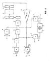
- the memory array of Fig. 1 comprises a multiplicity of recirculating CCD loops 1, 2 ... N which preferably are individually addressible for writing and reading purposes associated with the storage of digital data.
- the loops are individually addressible by respective loop select signals on lines 3 at the outputs of address decode 4.
- Loop address signals are applied via lines 5 from a source (not shown) located off chip 6 containing the loops.
- the serial bit outputs from each of the loops 1 through N are selectively applied to a respective shift register cell 1', 2' ... N' comprising shift register 7.
- Shift register 7 receives digital data from line 8 for the serial loading of the register stages.
- the data stored at any given time within register 7 can be serially shifted out via line 9 and driver circuit 10 and made available on output line 11.
- Shift register 7 is employed for the parallel data fetching and for the parallel data loading associated with the handling of data signals as well as test signals with the CCD loop memory array at different times.
- Apparatus is also provided for the serial data fetching and the serial data loading of an individually addressed loop.
- Input data is applied via line 31 in the presence of write commands on lines 34 and 48 supplied by command control 13.
- data stored within any addressed loop is fetched via lines 60, 61 and 62, AND gates 50, 51 and 52, OR gate 36 AND gate 37 (when conducting) and driver 38.
- Gate 37 is rendered conductive by a read command on line 39.
- Command signals for the fetching and storing of data in the array loops are applied by lines 12 to command control timing logic 13.
- Phase clocks for the control of shift register 7 and the array loops are applied by lines 14 to command control and timing logic 13.
- the phase clocks are of such frequency and phase to permit the entire shift register 7 to be loaded or unloaded in the time between the stepping of data from one bit position to the next position within each of the recirculating loops.
- Stepping clocks are applied to loops 1 through N via line 40.
- Shift clocks are applied to the individual shift register stages via line 15.
- Parallel read and parallel write commands are applied by lines 16 and 17, respectively, to the individual shift register stages.
- Parallel read command signals and serial read command signals are applied alternatively to lines 16 and 39, respectively, by command control 13. The same alternative application is made of the parallel write command signals and serial write command signals to lines 17 and 48, respectively.
- the typical CCD loop of Fig. 1 comprises AND circuit 18, OR circuit 19, series-parallel- series CCD registers 20, 21 and 22 and regenerative amplifier 23.
- AND circuit 25 produces a zero output which is inverted (26) to render AND circuit 18 conductive to each of the recirculating data bits.
- the recirculating loop is broken, by the non conductance of gate 18, upon the appearance of a write command on line 34.
- a signal appears on line 34 whenever a serial write command occurs on line 48 or a parallel write command occurs on line 17.
- Input data gate 27 conducts in the simultaneous presence of a respective parallel write command signal on line 17 and input data on line 29.
- the output of gate 27 is coupled into the loop via OR circuit 19.
- Data is read out of the recirculating loop via AND gate 30 and line 32 upon application of a parallel read command on line 16 and in the absence of a write command signal on line 34.
- Loop data signals are applied to AND gate 50 along with the respective loop selection signal on line 3.
- the output of gate 50 on line 49 is applied to OR gate 36.
- Write command signals are applied to AND gate 25 together with the respective loop selection signal on line 3.
- the serial input data bits are introduced into the loop via line 31 and OR circuit 19. The recirculating bits are blocked, during the writing interval by the non-conduction of gate 18 due to the conduction of gate 25 and the inversion provided by inverter 26, as previously explained.
Abstract
Description
- The present invention generally relates to means for fetching and storing data in a recirculating loop memory array and, more particularly, to shift register means for accomplishing those functions.
- In charge coupled device (CCD) memory arrays, multiple CCD loops are organized so as to be accessible via a single input pin and via a single output pin. Accordingly, the loops are accessed in serial succession. In those cases where the entire array is to be initialized to a predetermined state or tested to verify that the stored data is correct, sufficient time must be allocated to complete the serial accessing of the CCD loops. The required time increases objectionably as the CCD memory array increases in density to include larger numbers of individual loops. Direct parallel accessing of the individual CCD loops, on the other hand, permits much more rapid initialization, but only at the expense of requiring inacceptably large numbers of input-output (I/O) pins.
- Indirect parallel accessing of interior logic circuit points has been achieved via I/O pins according to a technique described in U.S.
Patent 3 783 254 to E. B. Eichelberger for "Level Sensitive Logic System", issued 1 January 1974 and in related U.S.Patents 3 761 695 and 3 784 907 to the same inventor. Briefly, clocked DC latches are provided at logic network nodes to be tested and additional circuitry is included to selectively connect the latches into a functional shift register. A predetermined pattern of binary ones and zeros can then be introduced serially into the shift register latches where they are retained for later use as parallel inputs to the logic network nodes to be tested. Additional clocked DC latches are provided at other logic network nodes to receive the signals representing the test results produced by the test signals introduced by the first clocked DC latches. Once the test results are stored in the second clocked DC latches, further circuitry connects the latches into a functional shift register which enables the test results to be shifted out. This technique, however, is not well suited for the dynamic testing of data stored within CCD loops within a memory array. - European patent application 81103610.2 for "Memory Array Fault Locator", filed 12 May 1981, inventors F. J. Aichel- mann, Jr. et al, discloses a technique for quickly determining (within designated subdivisions or partitions of recirculating type memory arrays) the locations of faulty bits received from the constituent recirculating type memory elements comprising the array. All loop memory elements are initialized to a predetermined condition for testing purposes by the loading of all loops with the same test data. The stored data is verified by means of a number of comparison gates. A distinctive signal is generated by a given comparison gate in the event that any one or more bits of the data received from one or more of the loops associated with the given comparison gate is non-identical to the data bits from all other associated loops. The output signals produced by the comparison gates are sensed in serial succession to locate the array subdivision containing any faulty elements. In one embodiment of the invention, a latch is provided at the output of each comparison gate. Each latch is set to store the information that one or more bits are faulty from the loops associated with that comparison gate. The latches are then sensed at logic speeds. The latches, however, perform no role in the storing of data within the recirculating loops nor do they participate in the fetching of data from the individual loops. The present invention intends to change that.
- Briefly, memory arrays of multiple recirculating loop memory elements are buffered for parallel fetching and loading operations by the provision of a shift register comprising a number of shift register cells equal in number to the number of recirculating elements in the array. Each recirculating element or loop is selectively connected to a respective shift register cell so that, on command, a particular recirculating bit in all of the loops can be fetched in parallel into their respective cells, and conversely, so that the bits stored in the shift register cells can be loaded in parallel into predetermined recirculating bits of their respective loops. By first loading all of the shift register cells with binary data, the corresponding bit in each of the recirculating loops can be loaded in parallel by selectively connecting the shift register cells to the recirculating loops. Then, the shift register is reloaded with new binary data and the next bit position in each of the recirculating loops is loaded in similar parallel fashion. This process is repeated until all of the bit positions in the recirculating loops have been loaded.
- Data fetching is accomplished in an analogous manner. That is, a given corresponding bit position in each of the recirculating loops is loaded into a respective shift register cell and then the shift register is emptied of its stored data by shifting. Then, the next bit in all of the recirculating loops is fetched into the respective cells of the shift register and the shift register is emptied as before.
- The shift register is operated at logic speeds which are much faster than the bit recirculating rate of the memory loops. Consequently, the entire shift register is loaded in the interval between successive steppings of the bits in the recirculating loops, provided that the number of recirculating loops and, hence, the length of the shift register is not too extensive. In the case of extensive loop arrays, the array can be partitioned into groups of a smaller number of loops with a correspondingly shortened shift register selectively connected to each of the loop groups.
- An embodiment of the invention is described below. The accompanying drawings show in
- Fig. 1 a simplified block diagram of a CCD memory array adapted for data fetching and storing in accordance with the present invention; and in
- Fig. 2 a simplified block diagram representing in greater detail a typical CCD loop of Fig. 1 and its selective connection to its respective shift register cell.
- The memory array of Fig. 1 comprises a multiplicity of recirculating
CCD loops lines 3 at the outputs ofaddress decode 4. Loop address signals are applied via lines 5 from a source (not shown) located offchip 6 containing the loops. The serial bit outputs from each of theloops 1 through N are selectively applied to a respective shift register cell 1', 2' ... N' comprisingshift register 7.Shift register 7 receives digital data from line 8 for the serial loading of the register stages. The data stored at any given time withinregister 7 can be serially shifted out vialine 9 anddriver circuit 10 and made available onoutput line 11.Shift register 7 is employed for the parallel data fetching and for the parallel data loading associated with the handling of data signals as well as test signals with the CCD loop memory array at different times. - Apparatus is also provided for the serial data fetching and the serial data loading of an individually addressed loop. Input data is applied via
line 31 in the presence of write commands onlines command control 13. Similarly, data stored within any addressed loop is fetched vialines gates gate 36 AND gate 37 (when conducting) and driver 38.Gate 37 is rendered conductive by a read command online 39. - Command signals for the fetching and storing of data in the array loops are applied by lines 12 to command
control timing logic 13. Phase clocks for the control ofshift register 7 and the array loops are applied bylines 14 to command control andtiming logic 13. The phase clocks are of such frequency and phase to permit theentire shift register 7 to be loaded or unloaded in the time between the stepping of data from one bit position to the next position within each of the recirculating loops. Stepping clocks are applied toloops 1 through N vialine 40. Shift clocks are applied to the individual shift register stages vialine 15. Parallel read and parallel write commands are applied bylines lines command control 13. The same alternative application is made of the parallel write command signals and serial write command signals tolines - Referring now to Fig. 2, the typical CCD loop of Fig. 1 comprises AND
circuit 18, ORcircuit 19, series-parallel-series CCD registers regenerative amplifier 23. When there is no write command online 34 during the read/write enable interval, ANDcircuit 25 produces a zero output which is inverted (26) to render ANDcircuit 18 conductive to each of the recirculating data bits. The recirculating loop is broken, by the non conductance ofgate 18, upon the appearance of a write command online 34. A signal appears online 34 whenever a serial write command occurs online 48 or a parallel write command occurs online 17.Input data gate 27 conducts in the simultaneous presence of a respective parallel write command signal online 17 and input data online 29. The output ofgate 27 is coupled into the loop via ORcircuit 19. Data is read out of the recirculating loop via ANDgate 30 andline 32 upon application of a parallel read command online 16 and in the absence of a write command signal online 34. - Loop data signals are applied to AND
gate 50 along with the respective loop selection signal online 3. The output ofgate 50 online 49 is applied toOR gate 36. Write command signals are applied to ANDgate 25 together with the respective loop selection signal online 3. The serial input data bits are introduced into the loop vialine 31 and ORcircuit 19. The recirculating bits are blocked, during the writing interval by the non-conduction ofgate 18 due to the conduction ofgate 25 and the inversion provided byinverter 26, as previously explained. - It can be seen from the preceding specification that provision is made, in accordance with the present invention, for the parallel accessing of any addressed loop for data storage and fetching purposes as well as for the serial accessing of all loops at the same time. In the former instance, one corresponding bit is extracted from each of the loops and is applied to the respective stage of an output shift register. The register is shifted at a high rate so that its contents may be emptied (or filled, as the case may be) in the time interval between successive steppings of the recirculating loop bits. The parallel loop accessing mode is of special importance when utilized either as a high speed storage testing facility or as a cache data buffer. It also provides a paging hierarchy organization whereby data is distributed between all loops rather than within a single loop.
Claims (6)
Applications Claiming Priority (2)
| Application Number | Priority Date | Filing Date | Title |
|---|---|---|---|
| US192581 | 1980-09-30 | ||
| US06/192,581 US4388701A (en) | 1980-09-30 | 1980-09-30 | Recirculating loop memory array having a shift register buffer for parallel fetching and storing |
Publications (3)
| Publication Number | Publication Date |
|---|---|
| EP0048810A2 true EP0048810A2 (en) | 1982-04-07 |
| EP0048810A3 EP0048810A3 (en) | 1985-09-11 |
| EP0048810B1 EP0048810B1 (en) | 1991-06-05 |
Family
ID=22710269
Family Applications (1)
| Application Number | Title | Priority Date | Filing Date |
|---|---|---|---|
| EP81106231A Expired EP0048810B1 (en) | 1980-09-30 | 1981-08-10 | Recirculating loop memory array with a shift register buffer |
Country Status (4)
| Country | Link |
|---|---|
| US (1) | US4388701A (en) |
| EP (1) | EP0048810B1 (en) |
| JP (1) | JPS5925316B2 (en) |
| DE (1) | DE3177245D1 (en) |
Cited By (7)
| Publication number | Priority date | Publication date | Assignee | Title |
|---|---|---|---|---|
| EP0363031A1 (en) * | 1988-09-20 | 1990-04-11 | Fujitsu Limited | Serial input/output semiconductor memory |
| US5142986A (en) * | 1990-07-20 | 1992-09-01 | Diehl Gmbh & Co. | Mine, particularly an anti-tank mine |
| US5760962A (en) * | 1993-02-26 | 1998-06-02 | Donnelly Corporation | Automatic rearview mirror system using a photosensor array |
| US6302545B1 (en) | 1993-02-26 | 2001-10-16 | Donnelly Corporation | Vehicle control system and method |
| US9940528B2 (en) | 2004-12-23 | 2018-04-10 | Magna Electronics Inc. | Driver assistance system for vehicle |
| US10726578B2 (en) | 2007-08-17 | 2020-07-28 | Magna Electronics Inc. | Vehicular imaging system with blockage determination and misalignment correction |
| US11091105B2 (en) | 2008-07-24 | 2021-08-17 | Magna Electronics Inc. | Vehicle vision system |
Families Citing this family (8)
| Publication number | Priority date | Publication date | Assignee | Title |
|---|---|---|---|---|
| US4750154A (en) * | 1984-07-10 | 1988-06-07 | Prime Computer, Inc. | Memory alignment system and method |
| JPS61289448A (en) * | 1985-06-18 | 1986-12-19 | Mitsubishi Electric Corp | Buffer memory device |
| JPH0628869A (en) * | 1992-05-12 | 1994-02-04 | Takayama:Kk | Meory device |
| JPH0628885A (en) * | 1992-06-23 | 1994-02-04 | Takayama:Kk | Memory device |
| WO2008024639A2 (en) | 2006-08-11 | 2008-02-28 | Donnelly Corporation | Automatic headlamp control system |
| US8451107B2 (en) | 2007-09-11 | 2013-05-28 | Magna Electronics, Inc. | Imaging system for vehicle |
| WO2009046268A1 (en) | 2007-10-04 | 2009-04-09 | Magna Electronics | Combined rgb and ir imaging sensor |
| US9489181B2 (en) * | 2014-10-09 | 2016-11-08 | National Instruments Corporation | Correlation analysis of program structures |
Citations (1)
| Publication number | Priority date | Publication date | Assignee | Title |
|---|---|---|---|---|
| US4024512A (en) * | 1975-06-16 | 1977-05-17 | Fairchild Camera And Instrument Corporation | Line-addressable random-access memory |
Family Cites Families (7)
| Publication number | Priority date | Publication date | Assignee | Title |
|---|---|---|---|---|
| JPS5130978B1 (en) * | 1971-03-05 | 1976-09-03 | ||
| US3784907A (en) * | 1972-10-16 | 1974-01-08 | Ibm | Method of propagation delay testing a functional logic system |
| US3783254A (en) * | 1972-10-16 | 1974-01-01 | Ibm | Level sensitive logic system |
| US3761695A (en) * | 1972-10-16 | 1973-09-25 | Ibm | Method of level sensitive testing a functional logic system |
| DE2729361A1 (en) * | 1976-07-29 | 1978-02-09 | Motorola Inc | MEMORY CIRCUIT |
| JPS5321541A (en) * | 1976-08-11 | 1978-02-28 | Nippon Telegr & Teleph Corp <Ntt> | Memory device |
| US4321694A (en) * | 1978-05-12 | 1982-03-23 | Burroughs Corporation | Charge coupled device memory with enhanced access features |
-
1980
- 1980-09-30 US US06/192,581 patent/US4388701A/en not_active Expired - Lifetime
-
1981
- 1981-07-20 JP JP56112393A patent/JPS5925316B2/en not_active Expired
- 1981-08-10 DE DE8181106231T patent/DE3177245D1/en not_active Expired - Fee Related
- 1981-08-10 EP EP81106231A patent/EP0048810B1/en not_active Expired
Patent Citations (1)
| Publication number | Priority date | Publication date | Assignee | Title |
|---|---|---|---|---|
| US4024512A (en) * | 1975-06-16 | 1977-05-17 | Fairchild Camera And Instrument Corporation | Line-addressable random-access memory |
Non-Patent Citations (3)
| Title |
|---|
| IBM TECHNICAL DISCLOSURE BULLETIN, vol. 13, no. 7, December 1970, page 1879, New York, US; W.K.HOFFMAN et al.: "Buffered shift register memory" * |
| IBM TECHNICAL DISCLOSURE BULLETIN, vol. 22, no. 10, March 1980, pages 4564-4565, New York, US; R.C.VARSHNEY: "CCD memory with testing capability" * |
| L'ONDE ELECTRIQUE, vol. 58, no. 4, April 1978, pages 312-318, Paris, FR; P.COEURE et al.: "Analyse et comparaison des possibilités d'emploi des mémoires à bulles et à transfert de charges * |
Cited By (15)
| Publication number | Priority date | Publication date | Assignee | Title |
|---|---|---|---|---|
| EP0363031A1 (en) * | 1988-09-20 | 1990-04-11 | Fujitsu Limited | Serial input/output semiconductor memory |
| US5142986A (en) * | 1990-07-20 | 1992-09-01 | Diehl Gmbh & Co. | Mine, particularly an anti-tank mine |
| US6953253B2 (en) | 1993-02-26 | 2005-10-11 | Donnelly Corporation | Vehicle photosensing control system |
| US6302545B1 (en) | 1993-02-26 | 2001-10-16 | Donnelly Corporation | Vehicle control system and method |
| US6523964B2 (en) | 1993-02-26 | 2003-02-25 | Donnelly Corporation | Vehicle control system and method |
| US6802617B2 (en) | 1993-02-26 | 2004-10-12 | Donnelly Corporation | Vehicle image capture system |
| US5760962A (en) * | 1993-02-26 | 1998-06-02 | Donnelly Corporation | Automatic rearview mirror system using a photosensor array |
| US8098142B2 (en) | 1993-02-26 | 2012-01-17 | Magna Mirrors Of America, Inc. | Vehicle monitoring system |
| US9940528B2 (en) | 2004-12-23 | 2018-04-10 | Magna Electronics Inc. | Driver assistance system for vehicle |
| US10509972B2 (en) | 2004-12-23 | 2019-12-17 | Magna Electronics Inc. | Vehicular vision system |
| US11308720B2 (en) | 2004-12-23 | 2022-04-19 | Magna Electronics Inc. | Vehicular imaging system |
| US10726578B2 (en) | 2007-08-17 | 2020-07-28 | Magna Electronics Inc. | Vehicular imaging system with blockage determination and misalignment correction |
| US11328447B2 (en) | 2007-08-17 | 2022-05-10 | Magna Electronics Inc. | Method of blockage determination and misalignment correction for vehicular vision system |
| US11908166B2 (en) | 2007-08-17 | 2024-02-20 | Magna Electronics Inc. | Vehicular imaging system with misalignment correction of camera |
| US11091105B2 (en) | 2008-07-24 | 2021-08-17 | Magna Electronics Inc. | Vehicle vision system |
Also Published As
| Publication number | Publication date |
|---|---|
| EP0048810B1 (en) | 1991-06-05 |
| JPS5925316B2 (en) | 1984-06-16 |
| EP0048810A3 (en) | 1985-09-11 |
| JPS5764393A (en) | 1982-04-19 |
| DE3177245D1 (en) | 1991-07-11 |
| US4388701A (en) | 1983-06-14 |
Similar Documents
| Publication | Publication Date | Title |
|---|---|---|
| US4404519A (en) | Testing embedded arrays in large scale integrated circuits | |
| KR960001948B1 (en) | Method and apparatus for programmable memory control with | |
| US3961252A (en) | Testing embedded arrays | |
| US4680733A (en) | Device for serializing/deserializing bit configurations of variable length | |
| US4933909A (en) | Dual read/write register file memory | |
| US4388701A (en) | Recirculating loop memory array having a shift register buffer for parallel fetching and storing | |
| US3037697A (en) | Information handling apparatus | |
| JPS6338728B2 (en) | ||
| US4450538A (en) | Address accessed memory device having parallel to serial conversion | |
| US4363124A (en) | Recirculating loop memory array tester | |
| US4326290A (en) | Means and methods for monitoring the storage states of a memory and other storage devices in a digital data processor | |
| US4696005A (en) | Apparatus for reducing test data storage requirements for high speed VLSI circuit testing | |
| GB1119626A (en) | Computer memory testing system | |
| EP0040219B1 (en) | Data processor having common monitoring and memory loading and checking means | |
| US5450455A (en) | Method and apparatus for including the states of nonscannable parts in a scan chain | |
| US4752907A (en) | Integrated circuit scanning apparatus having scanning data lines for connecting selected data locations to an I/O terminal | |
| KR19980087166A (en) | Tester pattern connection and looping method within automatic test device circuit tester | |
| EP0043902B1 (en) | Memory array fault locator | |
| US5339320A (en) | Architecture of circuitry for generating test mode signals | |
| KR100276504B1 (en) | Failure-data storage system | |
| AU643532B2 (en) | Data transfer interface module | |
| KR910014825A (en) | Data processing system and memory array testing processing method | |
| US4198699A (en) | Mass memory access method and apparatus | |
| US4575815A (en) | Data storage unit | |
| GB2128383A (en) | Data storage unit |
Legal Events
| Date | Code | Title | Description |
|---|---|---|---|
| PUAI | Public reference made under article 153(3) epc to a published international application that has entered the european phase |
Free format text: ORIGINAL CODE: 0009012 |
|
| 17P | Request for examination filed |
Effective date: 19810810 |
|
| AK | Designated contracting states |
Designated state(s): DE FR GB |
|
| PUAL | Search report despatched |
Free format text: ORIGINAL CODE: 0009013 |
|
| AK | Designated contracting states |
Designated state(s): DE FR GB |
|
| 17Q | First examination report despatched |
Effective date: 19870317 |
|
| GRAA | (expected) grant |
Free format text: ORIGINAL CODE: 0009210 |
|
| AK | Designated contracting states |
Kind code of ref document: B1 Designated state(s): DE FR GB |
|
| REF | Corresponds to: |
Ref document number: 3177245 Country of ref document: DE Date of ref document: 19910711 |
|
| PGFP | Annual fee paid to national office [announced via postgrant information from national office to epo] |
Ref country code: GB Payment date: 19910717 Year of fee payment: 11 |
|
| ET | Fr: translation filed | ||
| PGFP | Annual fee paid to national office [announced via postgrant information from national office to epo] |
Ref country code: FR Payment date: 19910726 Year of fee payment: 11 |
|
| PGFP | Annual fee paid to national office [announced via postgrant information from national office to epo] |
Ref country code: DE Payment date: 19910828 Year of fee payment: 11 |
|
| PLBE | No opposition filed within time limit |
Free format text: ORIGINAL CODE: 0009261 |
|
| STAA | Information on the status of an ep patent application or granted ep patent |
Free format text: STATUS: NO OPPOSITION FILED WITHIN TIME LIMIT |
|
| 26N | No opposition filed | ||
| PG25 | Lapsed in a contracting state [announced via postgrant information from national office to epo] |
Ref country code: GB Effective date: 19920810 |
|
| GBPC | Gb: european patent ceased through non-payment of renewal fee |
Effective date: 19920810 |
|
| PG25 | Lapsed in a contracting state [announced via postgrant information from national office to epo] |
Ref country code: FR Effective date: 19930430 |
|
| PG25 | Lapsed in a contracting state [announced via postgrant information from national office to epo] |
Ref country code: DE Effective date: 19930501 |
|
| REG | Reference to a national code |
Ref country code: FR Ref legal event code: ST |
|
| APAH | Appeal reference modified |
Free format text: ORIGINAL CODE: EPIDOSCREFNO |