EP0042977A1 - Batch placement system for electronic components or chips - Google Patents
Batch placement system for electronic components or chips Download PDFInfo
- Publication number
- EP0042977A1 EP0042977A1 EP81104009A EP81104009A EP0042977A1 EP 0042977 A1 EP0042977 A1 EP 0042977A1 EP 81104009 A EP81104009 A EP 81104009A EP 81104009 A EP81104009 A EP 81104009A EP 0042977 A1 EP0042977 A1 EP 0042977A1
- Authority
- EP
- European Patent Office
- Prior art keywords
- chip
- substrate
- chips
- batch
- placement system
- Prior art date
- Legal status (The legal status is an assumption and is not a legal conclusion. Google has not performed a legal analysis and makes no representation as to the accuracy of the status listed.)
- Granted
Links
Images


Classifications
-
- H—ELECTRICITY
- H01—ELECTRIC ELEMENTS
- H01L—SEMICONDUCTOR DEVICES NOT COVERED BY CLASS H10
- H01L21/00—Processes or apparatus adapted for the manufacture or treatment of semiconductor or solid state devices or of parts thereof
- H01L21/67—Apparatus specially adapted for handling semiconductor or electric solid state devices during manufacture or treatment thereof; Apparatus specially adapted for handling wafers during manufacture or treatment of semiconductor or electric solid state devices or components ; Apparatus not specifically provided for elsewhere
-
- Y—GENERAL TAGGING OF NEW TECHNOLOGICAL DEVELOPMENTS; GENERAL TAGGING OF CROSS-SECTIONAL TECHNOLOGIES SPANNING OVER SEVERAL SECTIONS OF THE IPC; TECHNICAL SUBJECTS COVERED BY FORMER USPC CROSS-REFERENCE ART COLLECTIONS [XRACs] AND DIGESTS
- Y10—TECHNICAL SUBJECTS COVERED BY FORMER USPC
- Y10T—TECHNICAL SUBJECTS COVERED BY FORMER US CLASSIFICATION
- Y10T29/00—Metal working
- Y10T29/49—Method of mechanical manufacture
- Y10T29/49002—Electrical device making
- Y10T29/49117—Conductor or circuit manufacturing
- Y10T29/49124—On flat or curved insulated base, e.g., printed circuit, etc.
- Y10T29/4913—Assembling to base an electrical component, e.g., capacitor, etc.
- Y10T29/49133—Assembling to base an electrical component, e.g., capacitor, etc. with component orienting
-
- Y—GENERAL TAGGING OF NEW TECHNOLOGICAL DEVELOPMENTS; GENERAL TAGGING OF CROSS-SECTIONAL TECHNOLOGIES SPANNING OVER SEVERAL SECTIONS OF THE IPC; TECHNICAL SUBJECTS COVERED BY FORMER USPC CROSS-REFERENCE ART COLLECTIONS [XRACs] AND DIGESTS
- Y10—TECHNICAL SUBJECTS COVERED BY FORMER USPC
- Y10T—TECHNICAL SUBJECTS COVERED BY FORMER US CLASSIFICATION
- Y10T29/00—Metal working
- Y10T29/49—Method of mechanical manufacture
- Y10T29/49764—Method of mechanical manufacture with testing or indicating
- Y10T29/49769—Using optical instrument [excludes mere human eyeballing]
-
- Y—GENERAL TAGGING OF NEW TECHNOLOGICAL DEVELOPMENTS; GENERAL TAGGING OF CROSS-SECTIONAL TECHNOLOGIES SPANNING OVER SEVERAL SECTIONS OF THE IPC; TECHNICAL SUBJECTS COVERED BY FORMER USPC CROSS-REFERENCE ART COLLECTIONS [XRACs] AND DIGESTS
- Y10—TECHNICAL SUBJECTS COVERED BY FORMER USPC
- Y10T—TECHNICAL SUBJECTS COVERED BY FORMER US CLASSIFICATION
- Y10T29/00—Metal working
- Y10T29/49—Method of mechanical manufacture
- Y10T29/49826—Assembling or joining
- Y10T29/49895—Associating parts by use of aligning means [e.g., use of a drift pin or a "fixture"]
-
- Y—GENERAL TAGGING OF NEW TECHNOLOGICAL DEVELOPMENTS; GENERAL TAGGING OF CROSS-SECTIONAL TECHNOLOGIES SPANNING OVER SEVERAL SECTIONS OF THE IPC; TECHNICAL SUBJECTS COVERED BY FORMER USPC CROSS-REFERENCE ART COLLECTIONS [XRACs] AND DIGESTS
- Y10—TECHNICAL SUBJECTS COVERED BY FORMER USPC
- Y10T—TECHNICAL SUBJECTS COVERED BY FORMER US CLASSIFICATION
- Y10T29/00—Metal working
- Y10T29/53—Means to assemble or disassemble
- Y10T29/5313—Means to assemble electrical device
- Y10T29/53174—Means to fasten electrical component to wiring board, base, or substrate
- Y10T29/53178—Chip component
-
- Y—GENERAL TAGGING OF NEW TECHNOLOGICAL DEVELOPMENTS; GENERAL TAGGING OF CROSS-SECTIONAL TECHNOLOGIES SPANNING OVER SEVERAL SECTIONS OF THE IPC; TECHNICAL SUBJECTS COVERED BY FORMER USPC CROSS-REFERENCE ART COLLECTIONS [XRACs] AND DIGESTS
- Y10—TECHNICAL SUBJECTS COVERED BY FORMER USPC
- Y10T—TECHNICAL SUBJECTS COVERED BY FORMER US CLASSIFICATION
- Y10T29/00—Metal working
- Y10T29/53—Means to assemble or disassemble
- Y10T29/5313—Means to assemble electrical device
- Y10T29/53261—Means to align and advance work part
Definitions
- the present invention relates generally to a system for accurately locating and positioning electrical or electronic items at identified sites on substrates and, more particularly, to an apparatus for accurately batch positioning electronic circuits, components or chips onto identified sites (footprints) on multichip module (MCM) substrates.
- MCM multichip module
- the substrate is prepared for the multiple chips by providing an array of chip sites with each chip site taking the form of a "footprint” or configuration of solder pads which match the electrical connections of the solder pad configuration on each of the respective chips.
- the solder pads of the chip are arranged on the same side of the chip as the chip components and may take the form of solder balls which are, after positioning on the substrate, bonded to corresponding substrate pads forming the "footprint".
- This invention intends to provide a remedy for these problems by providing a batch chip placement system for precisely batch positioning chips and the like upon a substrate containing an array of sites whose actual position on the substrate varies from the theoretical or nominal position over successive substrates.
- This positioning is achieved by first sensing the X and Y offsets of alignment marks on the substrate from their theoretical or nominal position. A first alignment mark is optically located and the X-Y alignment table holding the substrate is automatically servoed to null the offset and calculate the AX and AY correction factors. The process is repeated for a second alignment mark and the X-Y values of the two alignment marks are used to calculate the e and shrinkage factor corrections. The X, Y,8 and shrinkage factor corrections are then used to vary from nominal the X, Y, 8 and the spacing or periodicity parameters of prelocated chips relative to the module to obtain relative alignment of the chips to their sites on the substrate.
- the present invention provides an improved alignment and positioning system for aligning and positioning electronic components upon substrates, a system which is both automatic and precise and operates to predict correction factors required for accurate placement of the components upon a substrate.
- the batch chip placement system of this invention determines the X, Y, ⁇ and shrinkage factor corrections required to be made for accurate placement of batches of chips upon a substrate.
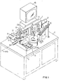
- the batch chip placement system of this invention shown enumerated generally at 1, is seen to include a cabinet arrangement 3 for supporting the electro-mechanical apparatus employed and for housing conventional control and processor circuitry. Chips are fed in parallel for positioning to chip pickup station 5 via parallel gravity feed chip banks 7A-7C. For purposes of simplicity, only 3 parallel feed chip banks are shown, but it is clear that any number of parallel chip feed banks may readily be employed, in accordance with the teachings of the present invention. Rather than be mounted on a gravity feed arrangement on chip feed base member 7, chip banks 7A-7C may be mounted on a base member which includes a linear vibrator arrangement which acts to vibrate the chips into position at the chip pickup station.
- chip typically includes transistors, diodes, resistors, capacitors, etc.
- integrated circuit typically includes transistors, diodes, resistors, capacitors, etc.
- the chips fed to chip pickup.station 5 are simultaneously picked up by vacuum pencil pickup assembly 9 and removed to batch shrink compensator 13.
- chips on batch shrink compensator 13 are simultaneously picked up by vacuum pencil assembly 11 and removed to substrate 15.
- vacuum pencil assemblies 9 and 11 work in synchronism, with the former simultaneously picking up chips from pickup station 5 and moving same to batch shrink compensator 13 while latter operates to pick up chips from batch shrink compensator 13 and remove same to substrate 15.
- Vacuum-pencil pickup assemblies 9 and 11 simultaneously move in the vertical direction on their respective tracks (not shown) in response to signals provided to servo motors 17 and 19, respectively. Tandem horizontal motion is imparted to pickup assemblies 9 and 11 by servo motor 21 driving horizontal transport assembly 23 on slider means, partially shown at 25A and 25B. Typically, servo motor 21 would rotate a lead screw arrangement, as shown at 27, to move assembly 23 in accordance with the directional signals given to the servo.
- Figure 1 shows the substrate positioned under optical alignment means 29, it is clear that after the alignment operation to determine the new X, Y and ⁇ values in accordance with the present invention, the substrate is moved on X-axis sliders 31 and 33 and Y-axis sliders (not shown) in response to signals applied to servo motor 35 and 36, respectively, to position X-Y substrate table 37 to a point which is in alignment with vacuum pencil assembly 11. In such position, chips picked up from batch shrink compensator 13 by vacuum assembly 11 may be transported and positioned in an appropriate manner on substrate 15.
- Optical alignment means 29 comprises a conventional arrangement of a standard vidicon camera 39, illumination source 41 and microscope 43.
- CRT graphic display device 45 is used to view the alignment operation wherein vidicon camera 39 scans, via microscope 43, the alignment mark illuminated by source 41.
- Electronic control of vidicon-camera 39 causes the camera to scan the alignment mark brought within its capture range and determine its center point. The center point of the alignment mark is then centered on CRT display 45 and the ⁇ X and ⁇ Y distances required to center the mark on the CRT are stored in the system's processor memory.
- any of a variety of conventional small general purpose processors may be employed to control the system described and process its information.
- an IBM Series 1 minicomputer may be used although microprocessors, such as the Intel 8048, may as readily be employed with required I/O and power supply apparatus. Since the operations to be controlled and calculations to be made in the batch chip placement system of the present invention are relatively simple and straightforward, it will be readily apparent to one skilled in' the art that standard routines using conventional programming languages and state of the art programming techniques may easily be employed in a number of different ways to program such processors for such operations and calculations.
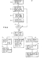
- the general block diagram arrangement shown in Figure 2 schematically depicts the overall manner in which the batch chip placement system, in accordance with the present.invention, operates to measure the deviation in X, Y, ⁇ and shrinkage factor E from their nominal values and feeds such information back to positioning means which act to place the chips, whereby the chips may precisely be positioned and. aligned with the actual footprint configuration appearing on the substrate. Description of such operation may more clearly be understood by reference to both Figures 1 and 2 and the sequence of steps shown in the flow diagram of Figure 6.
- the operator positions substrate 15 on X-Y table 37, shown in Figure 1.
- This step is depicted by block 49 in Figure 6.
- substrate 15 (in the example being considered) comprises a multi-chip module arrangement wherein 9 chips are to be positioned. Accurate registration of substrate 15 is achieved at this point by its being physically locked into position by four-point locator 47, shown in Figure 1. As shown, the four-point locator acts to align the four sides of the substrate with its four locating surfaces.
- the table moves to position the nominal location of the first alignment mark to be scanned under the optical center of optical alignment means 29.
- a pair of alignment marks at opposite sides of substrate 15 may accurately be positioned during substrate fabrication by forming the marks simultaneous with the formation of the array of "footprints" fcr the chips.
- the alignment marks are in a fixed position with respect to the "footprint” array and variations in the actual location of the alignment marks from their nominal location would apply equally well to the "footprints".
- variation in the position of the array of footprints from their nominal or.theoretical position may be introduced by mechanical error in the process step used to fabricate the footprints or variation from the nominal or theoretical shrinkage, as introduced during substrate sintering.
- a pair of chip "footprints" at opposing ends of the substrate may be employed as the alignment marks.
- footprints 15A and 15N may be utilized as the alignment marks to be scanned.
- these footprints are precisely located during the initial stages of fabricating the substrate, but subsequent forming, cutting and sintering steps act to cause the nominal location of the array of footprints to be misaligned with respect to the substrate edges.
- the system control circuitry at this point acts to cause the optical alignment means to scan the solder pads of footprint 15A to determine its optical center.
- processor control circuitry acts to move X-Y table 37 to position the actual center point of 15A with the center position of CRT display 45 (nominal position) and the ⁇ X and ⁇ Y distances required to center the optical center of footprint 15A on the CRT are stored in the system's processor memory, as hereinabove stated.
- This optical compare step is represented by block 55 in Figure 6.
- block 57 in Figure 6 where this is not the last chip site to be centered, the process is again repeated by returning to the step depicted by block 51. Accordingly, the optical alignment process again operates, this time on "footprint" 15N as shown in Figure 2, and the results are stored in the processor memory as represented by block 55.
- the system processor acts to appropriately add or subtract the ⁇ X's and ⁇ Y's to the nominal X and Y values of "footprints" 15A and 15N whereby the actual X/Y location of these marks or footprints with respect to the coordinate axis shown in Ficure 2 is determined.
- the predict and control function carried out by the system processor at this point is depicted by block 16 in Figure 2.
- the actual position of footprints 15A and 15N is employed by the processor to calculate ⁇ and the shrinkage factor E, as depicted by blocks 61 and 63 in Figure 6.
- any rotational or ⁇ misalignment may be computed as follows: where X A is the actual X value of "footprint” 15A, X N is the actual X value of "footprint” 15N, Y A is the actual Y value of "footprint” 15A and Y N is the actual value of "footprint” 15N.
- the shrinkage factor E may be computed as follows: where Y N and Y A are the actual Y values of "footprints" 15N and 15A and Y N (nominal) and Y A(nominal) are the nominal Y values of "footprints" 15N and 15A.
- Y N and Y A are the actual Y values of "footprints" 15N and 15A and Y N (nominal) and Y A(nominal) are the nominal Y values of "footprints" 15N and 15A.
- the nominal shrinkage factor may be used to find the predicted X value of chip sites on each side of the center chip sites used as alignment marks.
- batch chip compensator 13 in Figure 2 is not only used to correct for variations in actual "footprint" position from the nominal, but is also used to merge the chips closer together (or further apart) for positioning on the substrate. Since chip feed mechanism 5 has physical constraints or limits on locating the chips in very close proximity to one another, batch shrink compensator is provided to reduce the relative positioning of the chips as they appear
- the X value of the location of chip footprints on each side of center chip footprints 15A and 15N reflects not only correction for shrinkage factor E but also the amount of reduction required to merge the chips together for the close chip positioning used on substrate 15.
- the X values, X T , of the side chips, as corrected for shrinkage factor E may be determined as follows: where X (nominal) is the nominal X value of the chip site on the substrate and E is the shrinkage factor multiplier used to vary X (nominal) .
- X T values calculated for each chip site on opposing sides of center chip site 15A may be used for each successive row of chip placements since typically shrinkage in ceramic substrate material has been found to be linear and symmetrical about the center of the substrate. In this regard, shrinkage after sintering of 15 percent to 20 percent is not unusual.
- the actual X/Y values of the center chip location may be sent to batch shrink compensator 13, as shewn in Figure 2.
- the actual location of the center chip for each row of chips is employed as the reference point from which the locations of chips on opposing sides of the center chip may be determined.
- batch shrink compensator 13 Upon receiving the actual coordinates of the center chip footprint 15A, batch shrink compensator 13 positions chip locator 73 holding chip 24B, as shown in Figure 3, to the actual coordinate values of the center chip footprint.
- Chip locator 73 is positioned to the actual coordinate values of the center chip footprint via a servo motor and slide means, (not shown) to move the whole of batch chip compensator 13 to the appropriate cocrdi- nate position.
- the actual X/Y coordinate values of center chip footprint l5A are fed to compensator 13 via line 18.
- the ⁇ correction value is fed to batch shrink compensator 13 via line 20 and X T is fed via line 22'.
- the 9 correction value operates to cause a servo motor (not shown) to rotate shaft 75 the required number of degrees to correct for 9 misalignment.
- chip locators 77 and 79 may be positioned in accordance with the X T values, determined as hereinabove described. Operation of these steps is depicted by blocks 65 and 67 in Figure 6. Likewise, calculation of the shrinkage factor "E" is depicted by block 63 in Figure 6. After the periodicity or X T is calculated, as shown by block 69 in Figure 6, chip locators 77 and 79, as shown in Figure 3, are positioned in accordance with the calculated X values. This is depicted by block 71 in Figure 6.
- Chip locator 77 Positioning of chip locator 79, for example, as shown in Figure 6 is achieved through servo motor 81 acting upon gears 83 and 85 to rotate lead screw 89 whereby table 91 is appropriately positioned. Chip locator 77 operates in similar fashion. It is clear, however, that any of a variety of arrangements may readily be employed to appropriately move the chip locators.
- the batch shrink compensator depicted in Figure 2 illustrates the manner in which chips are moved from a separated position to a merged position, as is achieved by the operation of the servos in Figure 3.
- the chips in broken lines represent the chips positioned in a separated position in line with chip feed apparatus 5, and the chips in solid lines represent the same chips shown in broken lines in a merged position ready for pickup and placement on substrate 15'.
- the 3-row chip arrangement shown in Figure 2 it is clear that with the actual X/Y values of "footprints" 15A and 15N known, the footprint of the center chip in the center row may be determined by dividing the actual Y values of footprints 15A and 15N by 2. In such an arrangement, the shrinkage value E need not .
- the actual Y values of the center chip site in the rows between the first and last row would be accessed by incrementing from the first row an amount equal to the nominal distance between the first and second rows corrected for by shrinkage factor E, and so on. It should be appreciated that since the nominal periodicity between rows is constant and the shrinkage factor is constant, each successive row (after the positioning of the first row) may be found by incrementing a ccnstant or fixed amount from the previous row.
- chip placement proceeds in the following manner.
- batch shrink compensator 13 With batch shrink compensator 13 in its home position, i.e. with the chip locators in the expanded position and aligned with the tracks of chip feed pickup station 5, vacuum pencil 9, shown in Figure 1, removes chips from the chip feed and positions them in the respective chip locators. This is shown by the broken line chips in Figure 2.
- batch shrink compensator 13 is moved and positioned so that its center chip locator position corresponds to the actual X/Y position values determined. Data correction is then made and the chip locators on opposing sides of the center chip locator are moved to the calculated X value, as previously described.
- vacuum pencil - pickup 11 picks up the respective chips from their compensated position and linearly moves them to their respective "footprints" on substrate 15, now in its chip place position at the right in Figure 2.
- the compensator acts to position the chips in a configuration that matches the actual configuration of "footprints" on the substrate.
- the substrate upon which chips'are to be positioned is first measured to obtain parameter values indicative of the amount of deviation from what would be the nominal or theoretical configuration of "footprints" on the chip, correction values are then calculated for each footprint, rows of chips are positioned upon a compensator so that their positions may be adjusted to correspond to the actual positions of the "footprints" on the substrate and finally, the rows of chips are positioned in parallel upon their matching row of "footprints".
- the substrate X/Y table 37 may be moved so that the center chip site or "footprint" of the particular row in question is positioned in accordance with its actual X/Y values rather than its theoretical X/Y values.
- the center of t'he actual position of the center "footprint” is aligned with the center probe of vacuum pencil pickup assembly 11, as shown in Figure 1.
- the actual X/Y values fed to batch shrink .compensator 13 via line 18 are, instead, fed to servo motors 35 and 36 of the X/Y substrate table 37, shown in Figure 1.
- FIG 4 depicts a further diagramatic showing of the manner in which chip feed and pickup station 5 and batch shrink compensator 13 interact, in sequential fashion, to position the chips for final precise placement on substrate 15.
- Coarse chip positioning is first achieved through the action of chip feed tracks 7A-7C feeding the chips by gravity feed to chip pockets 8A-8C, as shown in Figure 4.
- the chip pockets are shown in more detail in Figure 4A.
- the chip feed track 7 narrows down to the size of the chip pocket 8, which is slightly larger than the X dimension of the chip.
- Adjustment screw 10 permits variable chip grid spacing to suit any product requirement.
- Adjustment screw 10 also facilitates Y alignment. If greater X position accuracy is required, a light finger spring or jet of air may readily be employed to drive the chips in chip pockets 8 against the pocket sidewall, thus fixing the X reference.
- Positioning in the Y direction for the coarse locating action of the chip feed and pickup station 5 is achieved through utilization of the leading edge of the chip abutting stop plate 12, shown in Figure 4A.
- the edge of chip 24 is employed as a reference in the coarse locating function carried out here, as opposed to employing the solder balls 26 as a reference.
- Self clean port 28 in Figure 4B is employed to keep the locating surface of stop plate 12 free of debris. Slot 30 beneath the self-cleaning port permits cleaning via air or vacuum.
- a fine chip locator function using solder balls, for example, as a reference is achieved by the action of chip locators 73, 77 and 79 positioned on batch shrink compensator 13., as previously described with reference to Figure 3.
- the detailed manner in which the fine chip locating function may be achieved will be described with reference to the chip locator structure shown in Figure 5. It is clear, however, that different locator structures may be employed where different workpiece items are to be positioned, in accordance with the particular application.
- slope surfaces 52 act to guide the solder balls of the chip into a precisely defined recess location.
- Spring clip structure 54 fits over locator body 56 to guide the edges of the chip so that the solder balls will be guided toward the top portions of slope surfaces 52.
- Figure 5A shows in more detail in Figure 5A wherein it can be seen that the edges of chip 24 are initially guided by the flanged portions 66 of spring clip 54.
- screw arrangement 58 permits the removal of the chip locator from batch shrink compensator 13 to accommodate cleaning, repair or change.
- Figure 5B shews a top view of the arrangement shown in Figures 5 and 5A. It should be appreciated that by separating the coarse chip locating function described in Figure 4 from the fine chip locating function described in Figure 5, the interference between these two functions is eliminated, and the physical limits seen in conventional designs constraining close positioning is avoided. In this regard, it should also be appreciated that as batch shrink compensator 13 merges the chips into a closely-spaced array or row, as hereinabove described, the flanged portions 66 of spring clips 54 may come into contact with one another. Because of the resilience of these flanged portions, close proximity of the chips is achieved, the limits of separation not being significantly greater than the thickness 60 of the spring clips. Accordingly, not only does batch shrink compensator 13 permit precise positioning of a complete row of chips with positional corrections being made for 6, X/Y coordinates and shrinkage factor, but batch shrink compensator also allows extremely close positioning of the chips as required for high density packaging.
- the arrangement in accordance with the present invention accommodates the high throughput requirements of modern technology.
- the batch shrink compensator arrangement described hereinabove permits positioning a complete row of chips upon a substrate, even higher throughput may be achieved through utilization of a multiplicity of batch shrink compensators operating in parallel.
- Such a typical parallel arrangement is shown in Figure 7.
- a substrate having a 5 X 5 array of chips is being fabricated.
- the assembly scheme utilizes five stations so that each row of the chip is positioned by a different station.
- Horizontal transport assemblies 123A-E used to transport chips from chip banks 107A-E to substrate 115, operate in a manner similar to horizontal transport assembly 23 shown in. Figure 1.
- Substrates are positioned at the various stations via conveyor belt 137.
- Blank substrates enter the system on a transport mechanism, such as conveyor belt 137, and are positioned under-optical alignment means 129 (designated optical chip reference module) in Figure 7.
- Optical alignment means 129 operates in a manner akin to optical alignment means 29 hereinabove described with respect to Figure 1.
- optical alignment means 129 operates to determine the actual X/Y position of a pair of alignment marks and the coordinates of the actual position of the pair of alignment marks is then utilized by electronic module 132 to calculate 9, shrinkage factor E and X T for each of the respective rows of chips to be positioned upon this substrate.
- the X/Y, ⁇ and X T values for each of the respective rows are sent to respective batch shrink compensators 113A-E at stations 1-5.
- electronic module 132 may comprise any of a variety of conventional data processing and control apparatus. Typically, an IBM Series I minicomputer may readily be employed to carry out the.operation described.
- conveyor belt 137 is incremented to the next substrate and optical alignment is again undertaken.
- the first row of chips is positioned on substrate 115A at station 1 in a manner akin to that with respect to Figure l.
- the respective stations position their assigned row of chips on the substrates with each of the stations operating in parallel such that when Station 5 positions the fifth row of chips upon the first substrate to appear, Station 1 is simultaneously applying the first row of chips to the fifth substrate to appear.
- conveyor belt 137 may position the filled substrates in an oven arrangement whereby the chip electrical contacts may be bonded to the substrate contacts.
- the scheme in Figure 7 increases throughput by a factor corresponding to the size of'the array of chips to be positioned.
- utilization of the arrangement of Figure 7 would increase throughput by approximately a factor of 3. It is also clear by the arrangement shown in Figure 7 that where stations in.excess of: the number required for a given substrate are provided, one station being down will not affect the entire line since the down station may be bypassed in favor of a spare station being utilized down line.
Abstract
Description
- The present invention relates generally to a system for accurately locating and positioning electrical or electronic items at identified sites on substrates and, more particularly, to an apparatus for accurately batch positioning electronic circuits, components or chips onto identified sites (footprints) on multichip module (MCM) substrates.
- In the fabrication of multichip modules for today's computers, electronic elements or components (e.g., transistors, diodes, capacitors, etc.) are closely integrated into the form of small "chips" which are mounted upon ceramic substrates. Before mounting the chips upon the substrate, the substrate is prepared for the multiple chips by providing an array of chip sites with each chip site taking the form of a "footprint" or configuration of solder pads which match the electrical connections of the solder pad configuration on each of the respective chips. Typically, the solder pads of the chip are arranged on the same side of the chip as the chip components and may take the form of solder balls which are, after positioning on the substrate, bonded to corresponding substrate pads forming the "footprint".
- With the trend toward smaller and smaller chips positioned in multiple form in closer and closer proximity to one another on a single substrate, chip handling and accurate chip placement on its "footprint" or site becomes more and more of a problem, particularly if it is desired to achieve automatic batch chip positioning on the substrate for high throughput. Compounding the problem is the fact that after the chip "footprints" or sites are created on the ceramic substrate, the substrate is fired for hardening and, as a result, a certain degree of shrinkage is introduced into the ceramic. Although the shrinkage within a given substrate is relatively uniform, the shrinkage factor varies considerably from substrate to substrate, thereby causing the chip site coordinates to vary from substrate to-substrate.
- In addition to variations in shrinkage factor, variations also exist from substrate to substrate in the orientation or alignment of chip sites and their X and Y offsets with respect to the edge of the substrate. These variations occur as.a result of the fact that although the respective location of sites may be positioned relatively accurately from site to site within a substrate, the position of the array of sites with reference to the substrate edge cannot be obtained with the same degree of accuracy. Accordingly, the X and Y coordinate offsets and rotation of the array of sites with respect to the substrate edge, along with the shrinkage factor, must be compensated for before accurate positioning can be obtained.
- Various efforts have been made in the prior art to align electronic components, such as chips and the like, for positioning on substrates. Typical of prior art efforts is that described by H. R. Rottman in U. S.
Patent 3 581 375, issued 1 June 1971. However, the Rottman system scans both chip and substrate to position one chip at a time and requires manual intervention. Likewise, U. S.Patent 3 840 978, issued 15 October 1974 to Lynch et al, describes an alignment system for positioning one chip at a time on a substrate utilizing manual techniques. - Further prior art efforts to align chips and the like to substrates is that described in U. S.
Patent 4 125 798, issued 14 November 1978, to Miller. Like Rottman and Lynch et al, Miller describes an arrangement for positioning one chip at a time on a substrate utilizing manual techniques. Another arrangement for positioning one chip at a time is that described by Atchley et al in U. S.Patent 4 116 348, issued 26 September 1978. Although Atchley et al describe a parallel feed arrangement for batch feeding of chips, the chips are picked up one at a time and positioned upon a substrate previously positioned to the proper X-Y location. - Although the prior art describes various arrangements for aligning chips to substrates, none of the prior art describes a high throughput arrangement for aligning multiple chips in a batch mode to a substrate, as described in accordance with the present invention. Gross batch positioning of wafers is described in U. S.
Patent 4 108 323 to Charles et al. However, Charles et al do not align their batch of wafers to any substrate arrangement but rather change the spacing between the wafers in accordance with the batch process step being undertaken. Thus, the wafers of the batch are spaced closely in a heat treatment step and then are spaced further apart, for example, in a subsequent chemical processing step. - Not only does the prior art fail to provide an arrangement for batch alignment and positioning of chips to wafers, it also fails to provide any arrangement for making predictions as to X, Y, 0 and shrinkage factor corrections required to accurately align chips to a substrate in an automatic mode.
- This invention intends to provide a remedy for these problems by providing a batch chip placement system for precisely batch positioning chips and the like upon a substrate containing an array of sites whose actual position on the substrate varies from the theoretical or nominal position over successive substrates.
- This positioning is achieved by first sensing the X and Y offsets of alignment marks on the substrate from their theoretical or nominal position. A first alignment mark is optically located and the X-Y alignment table holding the substrate is automatically servoed to null the offset and calculate the AX and AY correction factors. The process is repeated for a second alignment mark and the X-Y values of the two alignment marks are used to calculate the e and shrinkage factor corrections. The X, Y,8 and shrinkage factor corrections are then used to vary from nominal the X, Y, 8 and the spacing or periodicity parameters of prelocated chips relative to the module to obtain relative alignment of the chips to their sites on the substrate.
- Thus, the present invention provides an improved alignment and positioning system for aligning and positioning electronic components upon substrates, a system which is both automatic and precise and operates to predict correction factors required for accurate placement of the components upon a substrate.
- The batch chip placement system of this invention determines the X, Y, θ and shrinkage factor corrections required to be made for accurate placement of batches of chips upon a substrate.
- An embodiment of the invention is disclosed in the following description in connection with the drawings in which:
- Figure 1 shows a perspective view of the batch chip placement system in accordance with the present invention.
- Figure 2 shows a general block diagram arrangement depicting the overall manner in which the batch chip placement system operates.
- Figure 3 shows a detailed view of the batch shrink compensator used in the batch chip placement system of Figure 1.
- Figure 4 shows the manner in which chips' are fed in parallel to the batch shrink compensator for individual correction, placement'and subsequent batch positioning on a chip.
- Figures 5, 5A and 5B show the details of the fine chip locator feature used to locate and hold individual chips on the batch shrink compensator shown in Figure 4.
- Figure 6 shows a flow diagram of the sequence of steps involved.in batch positioning chips on a . substrate in accordance with the principles of the present invention.
- Figure 7 shows an extension of the batch chip placement system of Figure 1 for multiple batch chip placement.
- With reference now to the drawings and particularly to Figure 1, the batch chip placement system of this invention, shown enumerated generally at 1, is seen to include a
cabinet arrangement 3 for supporting the electro-mechanical apparatus employed and for housing conventional control and processor circuitry. Chips are fed in parallel for positioning tochip pickup station 5 via parallel gravityfeed chip banks 7A-7C. For purposes of simplicity, only 3 parallel feed chip banks are shown, but it is clear that any number of parallel chip feed banks may readily be employed, in accordance with the teachings of the present invention. Rather than be mounted on a gravity feed arrangement on chip feed base member 7,chip banks 7A-7C may be mounted on a base member which includes a linear vibrator arrangement which acts to vibrate the chips into position at the chip pickup station. Although reference is made herein to the term "chip", which typically includes transistors, diodes, resistors, capacitors, etc., in integrated circuit form, it is clear that discrete electrical elements or components such as these, as well as other'types of elements, may as readily be batch positioned, in accordance with the principles of the present invention. - Again, with reference to Figure 1, the chips fed to
chip pickup.station 5 are simultaneously picked up by vacuumpencil pickup assembly 9 and removed tobatch shrink compensator 13. In similar fashion, chips onbatch shrink compensator 13 are simultaneously picked up by vacuum pencil assembly 11 and removed tosubstrate 15. As can be seen, vacuum pencil assemblies 9 and 11 work in synchronism, with the former simultaneously picking up chips frompickup station 5 and moving same tobatch shrink compensator 13 while latter operates to pick up chips frombatch shrink compensator 13 and remove same tosubstrate 15. - Vacuum-pencil pickup assemblies 9 and 11 simultaneously move in the vertical direction on their respective tracks (not shown) in response to signals provided to
servo motors assemblies 9 and 11 by servo motor 21 drivinghorizontal transport assembly 23 on slider means, partially shown at 25A and 25B. Typically, servo motor 21 would rotate a lead screw arrangement, as shown at 27, to moveassembly 23 in accordance with the directional signals given to the servo. - Although Figure 1 shows the substrate positioned under optical alignment means 29, it is clear that after the alignment operation to determine the new X, Y and θ values in accordance with the present invention, the substrate is moved on
X-axis sliders servo motor batch shrink compensator 13 by vacuum assembly 11 may be transported and positioned in an appropriate manner onsubstrate 15. - Optical alignment means 29 comprises a conventional arrangement of a
standard vidicon camera 39,illumination source 41 and microscope 43. CRTgraphic display device 45 is used to view the alignment operation whereinvidicon camera 39 scans, via microscope 43, the alignment mark illuminated bysource 41. Electronic control of vidicon-camera 39 causes the camera to scan the alignment mark brought within its capture range and determine its center point. The center point of the alignment mark is then centered onCRT display 45 and the ΔX and ΔY distances required to center the mark on the CRT are stored in the system's processor memory. - It should be noted that'any of a variety of conventional small general purpose processors may be employed to control the system described and process its information. For example, an IBM Series 1 minicomputer may be used although microprocessors, such as the Intel 8048, may as readily be employed with required I/O and power supply apparatus. Since the operations to be controlled and calculations to be made in the batch chip placement system of the present invention are relatively simple and straightforward, it will be readily apparent to one skilled in' the art that standard routines using conventional programming languages and state of the art programming techniques may easily be employed in a number of different ways to program such processors for such operations and calculations.
- The general block diagram arrangement shown in Figure 2 schematically depicts the overall manner in which the batch chip placement system, in accordance with the present.invention, operates to measure the deviation in X, Y, θ and shrinkage factor E from their nominal values and feeds such information back to positioning means which act to place the chips, whereby the chips may precisely be positioned and. aligned with the actual footprint configuration appearing on the substrate. Description of such operation may more clearly be understood by reference to both Figures 1 and 2 and the sequence of steps shown in the flow diagram of Figure 6. Initially, the
operator positions substrate 15 on X-Y table 37, shown in Figure 1. This step is depicted byblock 49 in Figure 6. As can be seen, substrate 15 (in the example being considered) comprises a multi-chip module arrangement wherein 9 chips are to be positioned. Accurate registration ofsubstrate 15 is achieved at this point by its being physically locked into position by four-point locator 47, shown in Figure 1. As shown, the four-point locator acts to align the four sides of the substrate with its four locating surfaces. - As depicted by
block 51 in Figure 6, after the substrate has been positioned and located upon X-Y table 37 in Figure 1, the table moves to position the nominal location of the first alignment mark to be scanned under the optical center of optical alignment means 29. In this regard, a pair of alignment marks at opposite sides ofsubstrate 15 may accurately be positioned during substrate fabrication by forming the marks simultaneous with the formation of the array of "footprints" fcr the chips. By so doing, the alignment marks are in a fixed position with respect to the "footprint" array and variations in the actual location of the alignment marks from their nominal location would apply equally well to the "footprints". It should be understood that variation in the position of the array of footprints from their nominal or.theoretical position may be introduced by mechanical error in the process step used to fabricate the footprints or variation from the nominal or theoretical shrinkage, as introduced during substrate sintering. - Alternatively, rather than employ a pair of separate alignment marks, a pair of chip "footprints" at opposing ends of the substrate may be employed as the alignment marks. Thus, as shown in Figure 2,
footprints block 53 in Figure 6, the system control circuitry at this point acts to cause the optical alignment means to scan the solder pads offootprint 15A to determine its optical center. - After "footprint" 15A has been scanned by the optical system-to determine its optical center, processor control circuitry acts to move X-Y table 37 to position the actual center point of 15A with the center position of CRT display 45 (nominal position) and the ΔX and ΔY distances required to center the optical center of
footprint 15A on the CRT are stored in the system's processor memory, as hereinabove stated. This optical compare step is represented byblock 55 in Figure 6. As shown byblock 57 in Figure 6, where this is not the last chip site to be centered, the process is again repeated by returning to the step depicted byblock 51. Accordingly, the optical alignment process again operates, this time on "footprint" 15N as shown in Figure 2, and the results are stored in the processor memory as represented byblock 55. - As represented by
blocks Ficure 2 is determined. The predict and control function carried out by the system processor at this point is depicted byblock 16 in Figure 2. In accordance with such operation, the actual position offootprints blocks 
- Likewise, the shrinkage factor E may be computed as follows:

batch chip compensator 13 in Figure 2 is not only used to correct for variations in actual "footprint" position from the nominal, but is also used to merge the chips closer together (or further apart) for positioning on the substrate. Sincechip feed mechanism 5 has physical constraints or limits on locating the chips in very close proximity to one another, batch shrink compensator is provided to reduce the relative positioning of the chips as they appear atchip feed 5 down to the close positioning required for linear translation tosubstrate 15. - Thus, the X value of the location of chip footprints on each side of
center chip footprints substrate 15. The X values, XT, of the side chips, as corrected for shrinkage factor E, may be determined as follows:
- It should be noted that the XT values calculated for each chip site on opposing sides of
center chip site 15A may be used for each successive row of chip placements since typically shrinkage in ceramic substrate material has been found to be linear and symmetrical about the center of the substrate. In this regard, shrinkage after sintering of 15 percent to 20 percent is not unusual. - It should be appreciated that although description has been directed to the use of a pair of alignment marks, be they footprints or marks provided for alignment, any number of alignment marks may be used in accordance with the particular application. Thus, where a large chip array is being processed, it may be necessary to use several alignment marks for purposes of computing shrinkage E or X, Y and θ values for various sectors of the chip. Alternatively, it is possible to operate the system of the present invention to optically locate and determine the X, Y and θ values for every footprint, 'i.e. each chip site, on the substrate in a mapping-type mode.
- Some time during or after the calculation of θ and E, the actual X/Y values of the center chip location may be sent to batch shrink
compensator 13, as shewn in Figure 2. In this regard, the actual location of the center chip for each row of chips is employed as the reference point from which the locations of chips on opposing sides of the center chip may be determined. Upon receiving the actual coordinates of thecenter chip footprint 15A, batch shrinkcompensator 13positions chip locator 73holding chip 24B, as shown in Figure 3, to the actual coordinate values of the center chip footprint.Chip locator 73 is positioned to the actual coordinate values of the center chip footprint via a servo motor and slide means, (not shown) to move the whole ofbatch chip compensator 13 to the appropriate cocrdi- nate position. With reference to Figure 2, the actual X/Y coordinate values of center chip footprint l5A are fed to compensator 13 vialine 18. Likewise, the θ correction value is fed to batch shrinkcompensator 13 vialine 20 and XT is fed via line 22'. With reference to Figure 3, the 9 correction value operates to cause a servo motor (not shown) to rotateshaft 75 the required number of degrees to correct for 9 misalignment. - With
chip locator 73, in Figure 3, positioned at the actual X/Y coordinate values ofcenter chip footprint 15A and the compensator rotated about this X/Y position by θ degrees to correct for orientation errors,chip locators blocks block 63 in Figure 6. After the periodicity or XT is calculated, as shown byblock 69 in Figure 6,chip locators block 71 in Figure 6. Positioning ofchip locator 79, for example, as shown in Figure 6 is achieved throughservo motor 81 acting upongears Chip locator 77 operates in similar fashion. It is clear, however, that any of a variety of arrangements may readily be employed to appropriately move the chip locators. - It should be appreciated that the batch shrink compensator depicted in Figure 2 illustrates the manner in which chips are moved from a separated position to a merged position, as is achieved by the operation of the servos in Figure 3. Thus, the chips in broken lines represent the chips positioned in a separated position in line with
chip feed apparatus 5, and the chips in solid lines represent the same chips shown in broken lines in a merged position ready for pickup and placement on substrate 15'. With the 3-row chip arrangement shown in Figure 2, it is clear that with the actual X/Y values of "footprints" 15A and 15N known, the footprint of the center chip in the center row may be determined by dividing the actual Y values offootprints X 5 array, it is clear that the periodicity of the rows in the Y direction would need correction for variations in the nominal periodicity due to shrinkage value variations from the nominal. Thus, after having positioned the chip locator forchip site 15A to the actual position of the site, the location of the center chip in each subsequent row would be corrected in the Y direction in accordance with the shrinkage factor "E", i.e. variations in shrinkage factor from the nominal shrinkage factor. In such an arrangement, the actual Y values of the center chip site in the rows between the first and last row would be accessed by incrementing from the first row an amount equal to the nominal distance between the first and second rows corrected for by shrinkage factor E, and so on. It should be appreciated that since the nominal periodicity between rows is constant and the shrinkage factor is constant, each successive row (after the positioning of the first row) may be found by incrementing a ccnstant or fixed amount from the previous row. - With X/Y, 6 and XT determined, chip placement proceeds in the following manner. With batch shrink
compensator 13 in its home position, i.e. with the chip locators in the expanded position and aligned with the tracks of chipfeed pickup station 5,vacuum pencil 9, shown in Figure 1, removes chips from the chip feed and positions them in the respective chip locators. This is shown by the broken line chips in Figure 2. Thereafter, batch shrinkcompensator 13 is moved and positioned so that its center chip locator position corresponds to the actual X/Y position values determined. Data correction is then made and the chip locators on opposing sides of the center chip locator are moved to the calculated X value, as previously described. Thereafter, vacuum pencil - pickup 11 picks up the respective chips from their compensated position and linearly moves them to their respective "footprints" onsubstrate 15, now in its chip place position at the right in Figure 2. Thus, it can be seen that the compensator acts to position the chips in a configuration that matches the actual configuration of "footprints" on the substrate. - In summary, the substrate upon which chips'are to be positioned is first measured to obtain parameter values indicative of the amount of deviation from what would be the nominal or theoretical configuration of "footprints" on the chip, correction values are then calculated for each footprint, rows of chips are positioned upon a compensator so that their positions may be adjusted to correspond to the actual positions of the "footprints" on the substrate and finally, the rows of chips are positioned in parallel upon their matching row of "footprints".
- It should be appreciated that rather than move the whole batch shrink compensator so that the center chip of a row corresponds to the actual X/Y values, as an alternative, the substrate X/Y table 37 may be moved so that the center chip site or "footprint" of the particular row in question is positioned in accordance with its actual X/Y values rather than its theoretical X/Y values. Thus, the center of t'he actual position of the center "footprint" is aligned with the center probe of vacuum pencil pickup assembly 11, as shown in Figure 1. In accordance with such a scheme, the actual X/Y values fed to batch shrink .
compensator 13 vialine 18 are, instead, fed toservo motors - Figure 4 depicts a further diagramatic showing of the manner in which chip feed and
pickup station 5 and batch shrinkcompensator 13 interact, in sequential fashion, to position the chips for final precise placement onsubstrate 15. Coarse chip positioning is first achieved through the action of chip feed tracks 7A-7C feeding the chips by gravity feed to chippockets 8A-8C, as shown in Figure 4. The chip pockets are shown in more detail in Figure 4A. As shown there, the chip feed track 7 narrows down to the size of thechip pocket 8, which is slightly larger than the X dimension of the chip. Although only 3 banks of chips are being fed via the 3 tracks shown, it is clear that the modular design of the arrangement would readily permit expansion to additional tracks and chip pockets for parallel chip placement.Adjustment screw 10 permits variable chip grid spacing to suit any product requirement. Thus, the respective X locations of an array of chips and distances therebetween may be coarsely located through utilization ofadjustment screw 10.Adjustment screw 10 also facilitates Y alignment. If greater X position accuracy is required, a light finger spring or jet of air may readily be employed to drive the chips inchip pockets 8 against the pocket sidewall, thus fixing the X reference. - Positioning in the Y direction for the coarse locating action of the chip feed and
pickup station 5 is achieved through utilization of the leading edge of the chip abuttingstop plate 12, shown in Figure 4A. In this regard, it should be understood that where, for example, chips with solder balls are used, less precision is achieved using the chip's edge as a reference than would be achieved using the solder balls directly. This is shown more clearly in Figure 4B where the edge ofchip 24 is employed as a reference in the coarse locating function carried out here, as opposed to employing thesolder balls 26 as a reference. This is so due to the fact that, typically, dicing tolerances of the chip's edge are more coarse than solder ball tolerances. Selfclean port 28 in Figure 4B is employed to keep the locating surface ofstop plate 12 free of debris.Slot 30 beneath the self-cleaning port permits cleaning via air or vacuum. - A fine chip locator function using solder balls, for example, as a reference is achieved by the action of
chip locators - In the exploded view shown in Figure 5, slope surfaces 52 act to guide the solder balls of the chip into a precisely defined recess location.
Spring clip structure 54 fits overlocator body 56 to guide the edges of the chip so that the solder balls will be guided toward the top portions of slope surfaces 52. This is shown in more detail in Figure 5A wherein it can be seen that the edges ofchip 24 are initially guided by theflanged portions 66 ofspring clip 54. As hereinabove mentioned, since the location of the solder balls is given with more precision than the edges. ofchip 24 due to dicing tolerances, relatively fine positioning is achieved within the recess or pocket oflocator 56, independent of:chip edge. As is evident,screw arrangement 58 permits the removal of the chip locator from batch shrinkcompensator 13 to accommodate cleaning, repair or change. - Figure 5B shews a top view of the arrangement shown in Figures 5 and 5A. It should be appreciated that by separating the coarse chip locating function described in Figure 4 from the fine chip locating function described in Figure 5, the interference between these two functions is eliminated, and the physical limits seen in conventional designs constraining close positioning is avoided. In this regard, it should also be appreciated that as batch shrink
compensator 13 merges the chips into a closely-spaced array or row, as hereinabove described, theflanged portions 66 of spring clips 54 may come into contact with one another. Because of the resilience of these flanged portions, close proximity of the chips is achieved, the limits of separation not being significantly greater than thethickness 60 of the spring clips. Accordingly, not only does batch shrinkcompensator 13 permit precise positioning of a complete row of chips with positional corrections being made for 6, X/Y coordinates and shrinkage factor, but batch shrink compensator also allows extremely close positioning of the chips as required for high density packaging. - In addition to high density packaging and precise positioning, the arrangement in accordance with the present invention accommodates the high throughput requirements of modern technology. Although the batch shrink compensator arrangement described hereinabove permits positioning a complete row of chips upon a substrate, even higher throughput may be achieved through utilization of a multiplicity of batch shrink compensators operating in parallel. Such a typical parallel arrangement is shown in Figure 7. In the high throughput arrangement shown here, a substrate having a 5
X 5 array of chips is being fabricated. The assembly scheme utilizes five stations so that each row of the chip is positioned by a different station.Horizontal transport assemblies 123A-E, used to transport chips fromchip banks 107A-E to substrate 115, operate in a manner similar tohorizontal transport assembly 23 shown in. Figure 1. Substrates are positioned at the various stations viaconveyor belt 137. - Blank substrates enter the system on a transport mechanism, such as
conveyor belt 137, and are positioned under-optical alignment means 129 (designated optical chip reference module) in Figure 7. Optical alignment means 129 operates in a manner akin to optical alignment means 29 hereinabove described with respect to Figure 1. As previously described, optical alignment means 129 operates to determine the actual X/Y position of a pair of alignment marks and the coordinates of the actual position of the pair of alignment marks is then utilized byelectronic module 132 to calculate 9, shrinkage factor E and XT for each of the respective rows of chips to be positioned upon this substrate. The X/Y, θ and XT values for each of the respective rows are sent to respective batch shrink compensators 113A-E at stations 1-5. As hereinabove described,electronic module 132 may comprise any of a variety of conventional data processing and control apparatus. Typically, an IBM Series I minicomputer may readily be employed to carry out the.operation described. - After optical alignment has been completed,
conveyor belt 137 is incremented to the next substrate and optical alignment is again undertaken. At the same time, the first row of chips is positioned onsubstrate 115A atstation 1 in a manner akin to that with respect to Figure l. As successive chips progress along onconveyor belt 137, the respective stations position their assigned row of chips on the substrates with each of the stations operating in parallel such that whenStation 5 positions the fifth row of chips upon the first substrate to appear,Station 1 is simultaneously applying the first row of chips to the fifth substrate to appear. - It is clear that substrates having an increased array of chips would require a corresponding increase in a number-of stations. Likewise, a substrate having an increased array of chips would require an increase in the number of chip feed banks 107 and the number of vacuum pickup probes associated with
vacuum pickup assemblies - After positioning the last row of chips upon substrate 115,
conveyor belt 137 may position the filled substrates in an oven arrangement whereby the chip electrical contacts may be bonded to the substrate contacts. As can be seen, the scheme in Figure 7 increases throughput by a factor corresponding to the size of'the array of chips to be positioned. Thus, in the 3X 3 chip array hereinabove described, utilization of the arrangement of Figure 7 would increase throughput by approximately a factor of 3. It is also clear by the arrangement shown in Figure 7 that where stations in.excess of: the number required for a given substrate are provided, one station being down will not affect the entire line since the down station may be bypassed in favor of a spare station being utilized down line.
Claims (10)
Applications Claiming Priority (2)
| Application Number | Priority Date | Filing Date | Title |
|---|---|---|---|
| US06/163,671 US4342090A (en) | 1980-06-27 | 1980-06-27 | Batch chip placement system |
| US163671 | 1993-12-07 |
Publications (2)
| Publication Number | Publication Date |
|---|---|
| EP0042977A1 true EP0042977A1 (en) | 1982-01-06 |
| EP0042977B1 EP0042977B1 (en) | 1984-10-31 |
Family
ID=22591066
Family Applications (1)
| Application Number | Title | Priority Date | Filing Date |
|---|---|---|---|
| EP81104009A Expired EP0042977B1 (en) | 1980-06-27 | 1981-05-25 | Batch placement system for electronic components or chips |
Country Status (4)
| Country | Link |
|---|---|
| US (1) | US4342090A (en) |
| EP (1) | EP0042977B1 (en) |
| JP (1) | JPS5916408B2 (en) |
| DE (1) | DE3166926D1 (en) |
Cited By (13)
| Publication number | Priority date | Publication date | Assignee | Title |
|---|---|---|---|---|
| EP0146036A2 (en) * | 1983-12-12 | 1985-06-26 | International Business Machines Corporation | Method of forming multilayer ceramic substrates from large area green sheets |
| EP0162115A1 (en) * | 1983-09-22 | 1985-11-27 | Matsushita Electric Industrial Co., Ltd. | Method of mounting elements |
| EP0082613B1 (en) * | 1981-12-01 | 1986-01-15 | Mobil Oil Corporation | Process for producing alpha-picoline |
| GB2173426A (en) * | 1985-04-09 | 1986-10-15 | Dynapert Precima Ltd | Component placement machine |
| US4617728A (en) * | 1983-06-13 | 1986-10-21 | Sincotron Aps | Method and device for mounting electronic components on a printed circuit card |
| EP0109991B1 (en) * | 1982-11-30 | 1987-04-29 | International Business Machines Corporation | Gravity feed chute |
| EP0309118A2 (en) * | 1987-09-25 | 1989-03-29 | Micro Robotics Systems Inc. | Apparatus for and method of viewing surfaces |
| US5549716A (en) * | 1991-09-02 | 1996-08-27 | Tdk Corporation | Process for manufacturing integrated circuits using an automated multi-station apparatus including an adhesive dispenser and apparatus therefor |
| EP1564792A2 (en) * | 2004-02-13 | 2005-08-17 | Assembléon N.V. | Method and device for estimating a component placement position on a substrate |
| EP1544924A3 (en) * | 2003-12-19 | 2010-03-31 | Philips Lumileds Lighting Company LLC | LED package assembly |
| CN105397290A (en) * | 2015-12-14 | 2016-03-16 | 中国电子科技集团公司第四十八研究所 | Laser sealing welding machine for welding workpieces in batches and control method |
| CN109148311A (en) * | 2018-08-22 | 2019-01-04 | 重庆市嘉凌新科技有限公司 | Die-bonding device |
| CN114783865A (en) * | 2022-04-13 | 2022-07-22 | 苏州优力科瑞半导体科技有限公司 | Scribing and cutting method and system |
Families Citing this family (99)
| Publication number | Priority date | Publication date | Assignee | Title |
|---|---|---|---|---|
| CH636740A5 (en) * | 1980-05-19 | 1983-06-15 | Far Fab Assortiments Reunies | DEVICE FOR ALIGNING A WORKPIECE AND A SUBSTRATE. |
| US4459743A (en) * | 1980-12-05 | 1984-07-17 | J. Osawa Camera Sales Co., Ltd. | Automatic mounting apparatus for chip components |
| JPS57164310A (en) * | 1981-04-03 | 1982-10-08 | Hitachi Ltd | Automatic assembling device |
| NL8103574A (en) * | 1981-07-29 | 1983-02-16 | Philips Nv | METHOD AND APPARATUS FOR PLACING ELECTRICAL AND / OR ELECTRONIC COMPONENTS ON A SUBSTRATE. |
| DE3138296A1 (en) * | 1981-09-25 | 1983-04-28 | Siemens AG, 1000 Berlin und 8000 München | METHOD FOR POSITIONING AND FIXING OPTICAL COMPONENTS RELATIVELY TO OTHER |
| US4510575A (en) * | 1982-08-24 | 1985-04-09 | Aerodyne Research, Inc. | Method for writing holograms |
| US4550374A (en) * | 1982-11-15 | 1985-10-29 | Tre Semiconductor Equipment Corporation | High speed alignment method for wafer stepper |
| JPS59147942A (en) * | 1983-02-15 | 1984-08-24 | Nittan Co Ltd | Linkage control system for fume extracting machines |
| JPS6012550A (en) * | 1983-07-04 | 1985-01-22 | Nippon Kogaku Kk <Nikon> | Supplying device of mask for exposure transfer device |
| US4713784A (en) * | 1983-07-04 | 1987-12-15 | Canon Kabushiki Kaisha | Alignment apparatus |
| US4641257A (en) * | 1983-07-07 | 1987-02-03 | Canon Kabushiki Kaisha | Measurement method and apparatus for alignment |
| JPS60189517A (en) * | 1984-03-09 | 1985-09-27 | Mitsubishi Electric Corp | Position controller |
| US4531277A (en) * | 1984-04-12 | 1985-07-30 | At&T Technologies, Inc. | Assembling components having mating faces |
| US4780617A (en) * | 1984-08-09 | 1988-10-25 | Nippon Kogaku K.K. | Method for successive alignment of chip patterns on a substrate |
| FR2572619B1 (en) * | 1984-10-30 | 1986-12-26 | Ebauchesfabrik Eta Ag | METHOD FOR ASSEMBLING AND CONNECTING INTEGRATED CIRCUITS TO CIRCUIT UNITS AND MACHINE FOR IMPLEMENTING SAME |
| US4558812A (en) * | 1984-11-07 | 1985-12-17 | At&T Technologies, Inc. | Method and apparatus for batch solder bumping of chip carriers |
| US4617160A (en) * | 1984-11-23 | 1986-10-14 | Irvine Sensors Corporation | Method for fabricating modules comprising uniformly stacked, aligned circuit-carrying layers |
| EP0213206B1 (en) * | 1985-01-21 | 1993-09-01 | FUJI MACHINE Mfg. Co., Ltd. | Method of and apparatus for detecting electronic device-holding position and electronic device-mounting apparatus |
| US4856904A (en) * | 1985-01-21 | 1989-08-15 | Nikon Corporation | Wafer inspecting apparatus |
| USRE33974E (en) * | 1985-01-21 | 1992-06-30 | Fuji Machine Manufacturing Co., Ltd. | Method and apparatus for detecting hold-position of electronic component, and apparatus for mounting electronic component |
| DE3613229A1 (en) * | 1985-04-20 | 1986-10-23 | Fuji Photo Film Co., Ltd., Minami-Ashigara, Kanagawa | METHOD FOR DETECTING AND PROCESSING IMAGE INFORMATION |
| US4787143A (en) * | 1985-12-04 | 1988-11-29 | Tdk Corporation | Method for detecting and correcting failure in mounting of electronic parts on substrate and apparatus therefor |
| US4670981A (en) * | 1986-03-17 | 1987-06-09 | Nitto Kogyo Kabushiki Kaisha | Method of mounting electronic parts on the predetermined positions of a printed circuit board |
| JPS62263700A (en) * | 1986-05-09 | 1987-11-16 | 松下電器産業株式会社 | Electronic parts mounting |
| US4754545A (en) * | 1986-05-16 | 1988-07-05 | Western Digital Corporation | Component handling machine |
| US4809839A (en) * | 1986-05-16 | 1989-03-07 | Western Digital Corporation | Component handling machine |
| US4782273A (en) * | 1986-08-08 | 1988-11-01 | Control Data Corporation | Automatic part location and mechanical testing of part insertion |
| US4738025A (en) * | 1986-12-23 | 1988-04-19 | Northern Telecom Limited | Automated apparatus and method for positioning multicontact component |
| US4835704A (en) * | 1986-12-29 | 1989-05-30 | General Electric Company | Adaptive lithography system to provide high density interconnect |
| US4757933A (en) * | 1987-04-03 | 1988-07-19 | American Technology, Inc. | Ultrasonic weld location mask and method of use |
| US4876656A (en) * | 1987-08-28 | 1989-10-24 | Motorola Inc. | Circuit location sensor for component placement apparatus |
| GB8801897D0 (en) * | 1988-01-28 | 1988-02-24 | Dynapert Precima Ltd | Method of setting-up apparatus for handling electrical/electronic components |
| MY103662A (en) * | 1988-01-28 | 1993-08-28 | Emhart Ind | Method of setting up apparatus for handling electrical or electronic components |
| JPH01295500A (en) * | 1988-05-24 | 1989-11-29 | Taiyo Yuden Co Ltd | Mounting method for chip type electronic parts and apparatus therefor |
| CA1314085C (en) * | 1988-05-25 | 1993-03-02 | Andras G. Fule | Linear interpolation for a component placement robot |
| US4927069A (en) * | 1988-07-15 | 1990-05-22 | Sanken Electric Co., Ltd. | Soldering method capable of providing a joint of reduced thermal resistance |
| JPH0267739A (en) * | 1988-09-01 | 1990-03-07 | Mitsubishi Electric Corp | Method and apparatus for die bonding |
| US4899921A (en) * | 1988-10-28 | 1990-02-13 | The American Optical Corporation | Aligner bonder |
| WO1990005344A1 (en) * | 1988-11-02 | 1990-05-17 | Siemens Aktiengesellschaft | Process for placing modules on a support |
| JPH02165699A (en) * | 1988-12-20 | 1990-06-26 | Matsushita Electric Ind Co Ltd | Mounting method of flat package type ic using industrial robot |
| JPH071635Y2 (en) * | 1989-05-15 | 1995-01-18 | 株式会社オーク製作所 | Alignment table for automatic exposure equipment |
| US5094382A (en) * | 1990-03-14 | 1992-03-10 | Seiko Epson Corporation | Method of bonding leads to semiconductor elements |
| US5040291A (en) * | 1990-05-04 | 1991-08-20 | Universal Instruments Corporation | Multi-spindle pick and place method and apparatus |
| US5207467A (en) * | 1990-08-31 | 1993-05-04 | International Business Machines Corporation | Monitor for detecting the absence of an electronic component on a vacuum pickup |
| JP2966082B2 (en) * | 1990-11-06 | 1999-10-25 | 株式会社日立製作所 | Mounting order determination method and its mounting method |
| US5144747A (en) * | 1991-03-27 | 1992-09-08 | Integrated System Assemblies Corporation | Apparatus and method for positioning an integrated circuit chip within a multichip module |
| US5238174A (en) * | 1991-11-15 | 1993-08-24 | Kulicke And Soffa Investments, Inc. | Smart indexing head for universal lead frame work station |
| US5446960A (en) * | 1994-02-15 | 1995-09-05 | International Business Machines Corporation | Alignment apparatus and method for placing modules on a circuit board |
| US5914887A (en) * | 1994-04-19 | 1999-06-22 | Lsi Logic Corporation | Congestion based cost factor computing apparatus for integrated circuit physical design automation system |
| US5539652A (en) * | 1995-02-07 | 1996-07-23 | Hewlett-Packard Company | Method for manufacturing test simulation in electronic circuit design |
| WO1996036921A1 (en) * | 1995-05-19 | 1996-11-21 | 3Com Corporation | Method and apparatus for linking computer aided design databases with a numerical control machine database |
| JPH0982612A (en) * | 1995-09-18 | 1997-03-28 | Mitsubishi Electric Corp | Inspection method for superpositional deviation |
| US6405430B1 (en) * | 1996-02-07 | 2002-06-18 | Micron Technology, Inc. | Workpiece moving methods |
| US5892203A (en) * | 1996-05-29 | 1999-04-06 | International Business Machines Corporation | Apparatus for making laminated integrated circuit devices |
| US5831863A (en) * | 1996-06-28 | 1998-11-03 | Lsi Logic Corporation | Advanced modular cell placement system with wire length driven affinity system |
| US6085032A (en) * | 1996-06-28 | 2000-07-04 | Lsi Logic Corporation | Advanced modular cell placement system with sinusoidal optimization |
| US6067409A (en) * | 1996-06-28 | 2000-05-23 | Lsi Logic Corporation | Advanced modular cell placement system |
| US5872718A (en) * | 1996-06-28 | 1999-02-16 | Lsi Logic Corporation | Advanced modular cell placement system |
| US5914888A (en) * | 1996-06-28 | 1999-06-22 | Lsi Logic Corporation | Advanced modular cell placement system with coarse overflow remover |
| US5867398A (en) * | 1996-06-28 | 1999-02-02 | Lsi Logic Corporation | Advanced modular cell placement system with density driven capacity penalty system |
| US5844811A (en) * | 1996-06-28 | 1998-12-01 | Lsi Logic Corporation | Advanced modular cell placement system with universal affinity driven discrete placement optimization |
| US5870311A (en) * | 1996-06-28 | 1999-02-09 | Lsi Logic Corporation | Advanced modular cell placement system with fast procedure for finding a levelizing cut point |
| US5963455A (en) * | 1996-06-28 | 1999-10-05 | Lsi Logic Corporation | Advanced modular cell placement system with functional sieve optimization technique |
| US5808899A (en) * | 1996-06-28 | 1998-09-15 | Lsi Logic Corporation | Advanced modular cell placement system with cell placement crystallization |
| US5812740A (en) * | 1996-06-28 | 1998-09-22 | Lsi Logic Corporation | Advanced modular cell placement system with neighborhood system driven optimization |
| US5835381A (en) * | 1996-06-28 | 1998-11-10 | Lsi Logic Corporation | Advanced modular cell placement system with minimizing maximal cut driven affinity system |
| US5892688A (en) * | 1996-06-28 | 1999-04-06 | Lsi Logic Corporation | Advanced modular cell placement system with iterative one dimensional preplacement optimization |
| US6026223A (en) * | 1996-06-28 | 2000-02-15 | Scepanovic; Ranko | Advanced modular cell placement system with overlap remover with minimal noise |
| US5870312A (en) * | 1996-06-28 | 1999-02-09 | Lsi Logic Corporation | Advanced modular cell placement system with dispersion-driven levelizing system |
| US6030110A (en) * | 1996-06-28 | 2000-02-29 | Lsi Logic Corporation | Advanced modular cell placement system with median control and increase in resolution |
| US5943089A (en) * | 1996-08-23 | 1999-08-24 | Speedline Technologies, Inc. | Method and apparatus for viewing an object and for viewing a device that acts upon the object |
| JP3301347B2 (en) * | 1997-04-22 | 2002-07-15 | 松下電器産業株式会社 | Apparatus and method for mounting conductive ball |
| US6085407A (en) * | 1997-08-21 | 2000-07-11 | Micron Technology, Inc. | Component alignment apparatuses and methods |
| JP4215302B2 (en) * | 1998-08-03 | 2009-01-28 | 株式会社ディスコ | Recognition method of machining results |
| JP2001135995A (en) * | 1999-11-05 | 2001-05-18 | Matsushita Electric Ind Co Ltd | Device and method for mounting part |
| JP4937482B2 (en) * | 2000-05-22 | 2012-05-23 | 東レエンジニアリング株式会社 | Chip mounting apparatus and alignment method in the apparatus |
| US6543114B2 (en) * | 2001-03-08 | 2003-04-08 | Axsun Technologies, Inc. | Manufacturing system using solder self-alignment with optical component deformation fine alignment |
| US6545227B2 (en) | 2001-07-11 | 2003-04-08 | Mce/Kdi Corporation | Pocket mounted chip having microstrip line |
| US7023347B2 (en) * | 2002-08-02 | 2006-04-04 | Symbol Technologies, Inc. | Method and system for forming a die frame and for transferring dies therewith |
| US6776327B2 (en) * | 2002-11-05 | 2004-08-17 | Palomar Technologies, Inc. | High-accuracy placement method utilizing double pick and place |
| US7276388B2 (en) * | 2003-06-12 | 2007-10-02 | Symbol Technologies, Inc. | Method, system, and apparatus for authenticating devices during assembly |
| CN1906983B (en) * | 2004-01-15 | 2011-07-20 | 国际商业机器公司 | On-chip system |
| US20060225273A1 (en) * | 2005-03-29 | 2006-10-12 | Symbol Technologies, Inc. | Transferring die(s) from an intermediate surface to a substrate |
| US20070107186A1 (en) * | 2005-11-04 | 2007-05-17 | Symbol Technologies, Inc. | Method and system for high volume transfer of dies to substrates |
| DE112006003165T5 (en) * | 2005-11-29 | 2008-12-24 | Matsushita Electric Industrial Co., Ltd., Kadoma | Working device and working method for circuit boards |
| US7390681B1 (en) * | 2007-01-12 | 2008-06-24 | Advanced Micro Devices, Inc. | Derived metric for monitoring die placement |
| US7993940B2 (en) * | 2007-12-05 | 2011-08-09 | Luminus Devices, Inc. | Component attach methods and related device structures |
| US20090223628A1 (en) * | 2008-03-07 | 2009-09-10 | Semiconductor Energy Laboratory Co., Ltd. | Manufacturing apparatus of composite substrate and manufacturing method of composite substrate with use of the manufacturing apparatus |
| DE102009013353B3 (en) * | 2009-03-16 | 2010-10-07 | Siemens Aktiengesellschaft | Method for determining armor for constant tables of placement machines |
| FI20106357A0 (en) * | 2010-12-21 | 2010-12-21 | Valtion Teknillinen | Method and apparatus for an action directed to a portion of an electronic structure |
| JP2015509284A (en) * | 2011-12-28 | 2015-03-26 | エーファウ・グループ・エー・タルナー・ゲーエムベーハー | Method and apparatus for bonding a plurality of substrates |
| CN102683505A (en) * | 2012-05-17 | 2012-09-19 | 东莞宏威数码机械有限公司 | Vacuum disc type alignment system |
| JP5906399B2 (en) * | 2013-02-22 | 2016-04-20 | パナソニックIpマネジメント株式会社 | Electronic component mounting system and electronic component mounting method |
| US9165889B2 (en) * | 2013-06-28 | 2015-10-20 | Infineon Technologies Ag | Alignment mark definer |
| KR102595309B1 (en) * | 2016-07-20 | 2023-10-31 | 삼성전자주식회사 | method for detecting misalignment of chips, manufacturing method of fan-out panel level package using the same, and fan-out panel level package |
| US10643016B1 (en) * | 2017-12-19 | 2020-05-05 | Cadence Design Systems, Inc. | System, method and computer program product for design rule awareness associated with die and package electronic circuit co-design |
| CN112864037A (en) * | 2021-01-14 | 2021-05-28 | 长鑫存储技术有限公司 | Wafer measuring method, device, medium and electronic equipment |
| CN113857117B (en) * | 2021-09-01 | 2023-05-16 | 北京北方华创微电子装备有限公司 | Semiconductor process equipment and cleaning method |
| CN116453995B (en) * | 2023-06-16 | 2023-08-29 | 淄博美林电子有限公司 | Full-automatic IGBT production line |
Citations (3)
| Publication number | Priority date | Publication date | Assignee | Title |
|---|---|---|---|---|
| US3838274A (en) * | 1973-03-30 | 1974-09-24 | Western Electric Co | Electro-optical article positioning system |
| US4108323A (en) * | 1977-09-28 | 1978-08-22 | Rca Corporation | Machine for changing the spacing of a plurality of wafers |
| US4116348A (en) * | 1976-07-19 | 1978-09-26 | Deval Industries, Inc. | Component locating apparatus |
Family Cites Families (14)
| Publication number | Priority date | Publication date | Assignee | Title |
|---|---|---|---|---|
| US3590462A (en) * | 1968-11-18 | 1971-07-06 | Western Electric Co | Method and apparatus for expanding an array of articles |
| US3581375A (en) * | 1969-03-07 | 1971-06-01 | Ibm | Method and apparatus for manufacturing integrated circuits |
| US3611561A (en) * | 1969-04-21 | 1971-10-12 | Paul A Dosier | Transfer mechanism with loading nest |
| US3840978A (en) * | 1969-11-12 | 1974-10-15 | Ibm | Method for positioning and bonding |
| US3722062A (en) * | 1971-11-04 | 1973-03-27 | Warwick Electronics Inc | Component insertion system |
| US3909933A (en) * | 1973-03-30 | 1975-10-07 | Western Electric Co | Method for transferring and bonding articles |
| US4040169A (en) * | 1974-03-04 | 1977-08-09 | Watkins-Johnson Co. | Method of fabricating an array of semiconductor devices |
| US3930295A (en) * | 1974-03-04 | 1976-01-06 | Signetics Corporation | Tool for fabricating diode array |
| US3903363A (en) * | 1974-05-31 | 1975-09-02 | Western Electric Co | Automatic positioning system and method |
| US3988535A (en) * | 1975-11-04 | 1976-10-26 | Western Electric Company, Inc. | Automated positioning |
| FR2365209A1 (en) * | 1976-09-20 | 1978-04-14 | Cii Honeywell Bull | PROCESS FOR THE ASSEMBLY OF MICRO-PLATES OF INTEGRATED CIRCUITS ON A SUBSTRATE AND INSTALLATION FOR ITS IMPLEMENTATION |
| US4063347A (en) * | 1976-10-01 | 1977-12-20 | Usm Corporation | Machine for inserting multi-lead components sequentially |
| US4125798A (en) * | 1977-04-11 | 1978-11-14 | Miller C Fredrick | Method and means for locating process points on miniaturized circuits |
| US4151945A (en) * | 1977-12-08 | 1979-05-01 | Universal Instruments Corporation | Automated hybrid circuit board assembly apparatus |
-
1980
- 1980-06-27 US US06/163,671 patent/US4342090A/en not_active Expired - Lifetime
-
1981
- 1981-05-14 JP JP56071519A patent/JPS5916408B2/en not_active Expired
- 1981-05-25 EP EP81104009A patent/EP0042977B1/en not_active Expired
- 1981-05-25 DE DE8181104009T patent/DE3166926D1/en not_active Expired
Patent Citations (3)
| Publication number | Priority date | Publication date | Assignee | Title |
|---|---|---|---|---|
| US3838274A (en) * | 1973-03-30 | 1974-09-24 | Western Electric Co | Electro-optical article positioning system |
| US4116348A (en) * | 1976-07-19 | 1978-09-26 | Deval Industries, Inc. | Component locating apparatus |
| US4108323A (en) * | 1977-09-28 | 1978-08-22 | Rca Corporation | Machine for changing the spacing of a plurality of wafers |
Non-Patent Citations (3)
| Title |
|---|
| IBM TECHNICAL DISCLOSURE BULLETIN, Vol. 20, No. 9, February 1978, New York, CACCOMA et al. "Chip Orientor with Shrink Compensation for Gang Placement" pages 3449 to 3451 * |
| IBM TECHNICAL DISCLOSURE BULLETIN, Vol. 22, No. 7, December 1979, New York, K.G. HOEBENER "Multiple Size Chip Pickup, Orientation and Placement Station" pages 2757 to 2761 * |
| Patents Abstracts of Japan Vol. 2, No. 37, 13 March 1978, page 72E78 & JP-A-53 003 165 * |
Cited By (17)
| Publication number | Priority date | Publication date | Assignee | Title |
|---|---|---|---|---|
| EP0082613B1 (en) * | 1981-12-01 | 1986-01-15 | Mobil Oil Corporation | Process for producing alpha-picoline |
| EP0109991B1 (en) * | 1982-11-30 | 1987-04-29 | International Business Machines Corporation | Gravity feed chute |
| US4617728A (en) * | 1983-06-13 | 1986-10-21 | Sincotron Aps | Method and device for mounting electronic components on a printed circuit card |
| EP0162115A1 (en) * | 1983-09-22 | 1985-11-27 | Matsushita Electric Industrial Co., Ltd. | Method of mounting elements |
| EP0162115A4 (en) * | 1983-09-22 | 1986-02-20 | Matsushita Electric Ind Co Ltd | Method of mounting elements. |
| EP0146036A2 (en) * | 1983-12-12 | 1985-06-26 | International Business Machines Corporation | Method of forming multilayer ceramic substrates from large area green sheets |
| EP0146036A3 (en) * | 1983-12-12 | 1987-01-14 | International Business Machines Corporation | Method of forming multilayer ceramic substrates from large area green sheets |
| GB2173426A (en) * | 1985-04-09 | 1986-10-15 | Dynapert Precima Ltd | Component placement machine |
| EP0309118A2 (en) * | 1987-09-25 | 1989-03-29 | Micro Robotics Systems Inc. | Apparatus for and method of viewing surfaces |
| EP0309118A3 (en) * | 1987-09-25 | 1990-08-01 | Micro Robotics Systems Inc. | Apparatus for and method of viewing surfaces |
| US5549716A (en) * | 1991-09-02 | 1996-08-27 | Tdk Corporation | Process for manufacturing integrated circuits using an automated multi-station apparatus including an adhesive dispenser and apparatus therefor |
| EP1544924A3 (en) * | 2003-12-19 | 2010-03-31 | Philips Lumileds Lighting Company LLC | LED package assembly |
| EP1564792A2 (en) * | 2004-02-13 | 2005-08-17 | Assembléon N.V. | Method and device for estimating a component placement position on a substrate |
| EP1564792A3 (en) * | 2004-02-13 | 2006-11-02 | Assembléon N.V. | Method and device for estimating a component placement position on a substrate |
| CN105397290A (en) * | 2015-12-14 | 2016-03-16 | 中国电子科技集团公司第四十八研究所 | Laser sealing welding machine for welding workpieces in batches and control method |
| CN109148311A (en) * | 2018-08-22 | 2019-01-04 | 重庆市嘉凌新科技有限公司 | Die-bonding device |
| CN114783865A (en) * | 2022-04-13 | 2022-07-22 | 苏州优力科瑞半导体科技有限公司 | Scribing and cutting method and system |
Also Published As
| Publication number | Publication date |
|---|---|
| EP0042977B1 (en) | 1984-10-31 |
| JPS5916408B2 (en) | 1984-04-16 |
| US4342090A (en) | 1982-07-27 |
| DE3166926D1 (en) | 1984-12-06 |
| JPS5715436A (en) | 1982-01-26 |
Similar Documents
| Publication | Publication Date | Title |
|---|---|---|
| EP0042977B1 (en) | Batch placement system for electronic components or chips | |
| US4980971A (en) | Method and apparatus for chip placement | |
| KR102196105B1 (en) | Electronic component mounting device and mounting method, and method for manufacturing package component | |
| US5040291A (en) | Multi-spindle pick and place method and apparatus | |
| EP0708587B1 (en) | Method and apparatus for mounting a part at a specific position | |
| EP1251550A1 (en) | Method and apparatus for automatically positioning electronic die within component packages | |
| US5068588A (en) | Apparatus for mounting a flat package type ic | |
| US6563530B1 (en) | Camera position-correcting method and system and dummy component for use in camera position correction | |
| US6538425B1 (en) | Method of measuring accuracy of electric-component mounting system | |
| US3843036A (en) | Apparatus for bonding a beam-lead device to a substrate | |
| WO1997038567A1 (en) | Method of placing a component on a substrate and component placement machine for carrying out the method | |
| KR100447310B1 (en) | Mounting device and component-mounting method thereof | |
| US6983872B2 (en) | Substrate alignment method and apparatus | |
| US4633584A (en) | Accurate positioning of solid components for a robotic pickup | |
| JP4562275B2 (en) | Electrical component mounting system and accuracy inspection method thereof | |
| KR102417464B1 (en) | Electronic component bonding apparatus | |
| JP7112274B2 (en) | Mounting equipment and calibration substrates used for mounting equipment | |
| JPH01155698A (en) | Electronic component packaging device | |
| JP2000138240A (en) | Moving device of position recognizing means | |
| JPH05109788A (en) | Die bonding device | |
| JPH02278166A (en) | Apparatus for inspecting semiconductor | |
| JPH02281101A (en) | Semiconductor inspecting apparatus | |
| JP2784793B2 (en) | Semiconductor inspection apparatus and semiconductor element alignment method | |
| JPH0446693B2 (en) | ||
| JPH02281159A (en) | Semiconductor inspection apparatus |
Legal Events
| Date | Code | Title | Description |
|---|---|---|---|
| PUAI | Public reference made under article 153(3) epc to a published international application that has entered the european phase |
Free format text: ORIGINAL CODE: 0009012 |
|
| 17P | Request for examination filed |
Effective date: 19811027 |
|
| AK | Designated contracting states |
Designated state(s): DE FR GB |
|
| GRAA | (expected) grant |
Free format text: ORIGINAL CODE: 0009210 |
|
| AK | Designated contracting states |
Designated state(s): DE FR GB |
|
| REF | Corresponds to: |
Ref document number: 3166926 Country of ref document: DE Date of ref document: 19841206 |
|
| ET | Fr: translation filed | ||
| PLBE | No opposition filed within time limit |
Free format text: ORIGINAL CODE: 0009261 |
|
| STAA | Information on the status of an ep patent application or granted ep patent |
Free format text: STATUS: NO OPPOSITION FILED WITHIN TIME LIMIT |
|
| 26N | No opposition filed | ||
| PGFP | Annual fee paid to national office [announced via postgrant information from national office to epo] |
Ref country code: GB Payment date: 19950413 Year of fee payment: 15 |
|
| PGFP | Annual fee paid to national office [announced via postgrant information from national office to epo] |
Ref country code: FR Payment date: 19950427 Year of fee payment: 15 |
|
| PGFP | Annual fee paid to national office [announced via postgrant information from national office to epo] |
Ref country code: DE Payment date: 19950524 Year of fee payment: 15 |
|
| PG25 | Lapsed in a contracting state [announced via postgrant information from national office to epo] |
Ref country code: GB Effective date: 19960525 |
|
| GBPC | Gb: european patent ceased through non-payment of renewal fee |
Effective date: 19960525 |
|
| PG25 | Lapsed in a contracting state [announced via postgrant information from national office to epo] |
Ref country code: FR Effective date: 19970131 |
|
| PG25 | Lapsed in a contracting state [announced via postgrant information from national office to epo] |
Ref country code: DE Effective date: 19970201 |
|
| REG | Reference to a national code |
Ref country code: FR Ref legal event code: ST |