EP0033412A2 - Method and apparatus for speech recognition - Google Patents
Method and apparatus for speech recognition Download PDFInfo
- Publication number
- EP0033412A2 EP0033412A2 EP80303965A EP80303965A EP0033412A2 EP 0033412 A2 EP0033412 A2 EP 0033412A2 EP 80303965 A EP80303965 A EP 80303965A EP 80303965 A EP80303965 A EP 80303965A EP 0033412 A2 EP0033412 A2 EP 0033412A2
- Authority
- EP
- European Patent Office
- Prior art keywords
- signal
- signals
- frequency
- producing
- relational
- Prior art date
- Legal status (The legal status is an assumption and is not a legal conclusion. Google has not performed a legal analysis and makes no representation as to the accuracy of the status listed.)
- Ceased
Links
Images


Classifications
-
- G—PHYSICS
- G10—MUSICAL INSTRUMENTS; ACOUSTICS
- G10L—SPEECH ANALYSIS OR SYNTHESIS; SPEECH RECOGNITION; SPEECH OR VOICE PROCESSING; SPEECH OR AUDIO CODING OR DECODING
- G10L15/00—Speech recognition
Definitions
- the field of the invention relates to the electronic recognition of speech and more particularly to a method and apparatus for recognizing speech based on the relational characteristics of signal components comprising the speech signal.
- speech recognition circuitry coupled with a computer can be used to great advantage in a wide variety of tasks.
- the interface between a computer and a human operator has been a mechanical keyboard.
- a keyboard interface has a number of disadvantages including slow speed, expense, the need for training for the operator and the limitations that the operators hands are fully occupied and cannot be used for other purposes.
- the present invention can be embodied.in a method and apparatus for producing a template to represent an audio signal so that a given audio signal can be compared for example, with a dictionary of scored templates, representing audio signals in order to identify the unknown audio signal.
- Each of the stored audio signals includes the word or phrase represented by the signal.
- the present invention provides for the recognition of speech for the production of corresponding text.
- the present invention provides a method for producing a template to represent an audio signal comprising the steps of extracting a plurality of signal components from the audio signal, producing one or more relational signals each of which is proportional to a plurality of said signal components, and storing the relational signals to serve as the templates which represent each of the audio signals.
- the invention also provides apparatus for producing a template to represent an audio signal comprising:
- the present invention comprises a method and apparatus for the recognition of human speech.
- FIGURE 1 there is shown a block diagram of a first embodiment of the speech recognition apparatus of the present invention.
- a speech recognition circuit 10 receives human speech at a microphone 12 which generates an audio signal that is transferred sequentially through an audio preamplifier 14 and an audio level limiter 16.
- the audio signal generated at the output of limiter 16 is provided as inputs to a low frequency band pass filter 18 and a high frequency band pass filter 20.
- Filter 18 is designed to have a pass band covering the range of 300 to 1100 Hz.
- High frequency filter 20 is designed to have a pass band in the range of 1500 to 4500 Hz.
- the low frequency component P 1 of the input audio signal is produced as the output of band pass filter 18 and the high frequency component P 2 of the input audio signal is produced as the output of band pass filter 20.
- the low frequency audio component P 1 from filter 18 is input to both a comparator and pulse generator 22 and a precision rectifier 24.
- the comparator and pulse generator 22 the low frequency component audio signal P i is zero crossing detected to generate a pulse train corresponding to the frequency of audio signal P 1 .
- the pulse train generated by circuit 22 is passed through a low pass filter 26 which produces a DC voltage F 1 on line 28, the signal F 1 being proportional to the instantaneous frequency of the audio signal component P 1 input to comparator and pulse generator 22.
- the low frequency audio signal P 1 is rectified in circuit 24 and the rectified signal is passed through a low pass filter 30 to generate a DC amplitude signal A 1 on line 32.
- Signal A 1 is proportional to the amplitude of the low frequency audio signal P 1 produced at the output of filter 18.
- the high frequency audio component P 2 received from the high frequency filter 20 is input to both a comparator and pulse generator 34 and a precision rectifier 36. Within the comparator and pulse generator 34 the high frequency component signal P 2 is zero crossing detected to produce a pulse train corresponding to the frequency of signal P2.. The pulse train is input to a low pass filter 38 to generate a DC signal F 2 on line 40. Signal F 2 is a DC voltage which is proportional to the frequency of the high frequency audio signal component P 2 .
- the high frequency component P 2 of the audio signal which is extracted by the filter 20 is supplied as an input to precision rectifier 36 and the rectified output thereof is input to a low pass filter 42 to produce a signal A 2 on line 44, signal A 2 being proportional to the amplitude of the high frequency signal P2.
- Each of the-DC signals F 1 , F 2 , A 1 and A 2 are input to an analog multiplexer 48. These analog signals are selectively routed by-multiplexer 48 so that they are provided to a scaled product detector 50 and a scaled ratio detector 52. The analog signals are routed in a time sequence controlled by clock signals provided by a timing oscillator 54.
- the scaled product detector 50 produces two analog output signals. These are ignals M 1 and M 2 . Signal M 1 is proportional to the product of the frequency signals F 1 and F 2 . Signal M 2 is proportional to the product of the amplitude signals A l and A 2 .
- the scaled ratio detector 52 produces signals R 1 and R 2 where R 1 is proportional to the ratio of F 2 to F1 and R2 is the ratio of A 1 to A 2 7
- the signals M 1 , M 2 , R 1 and R 2 are defined as follows:
- the constants k 1 , k 2 , k 3 and k 4 are selectable by the operator.
- the constants k 1 , k 2 , k 3 and k 4 are provided as scaling factors.
- the product signals M 1 and M 2 from the scaled product detector 50 are input sequentially to an analog multiplexer 56.
- the ratio signals R 1 and R 2 from the scaled ratio detector 52 are sequentially input to analog multiplexer 56.
- the clock signals generated by timing oscillator 54 are also provided to multiplexer 56 to provide coordinated sequential operation.
- the signals provided as inputs to analog multiplexer 56 are sequentially routed through line 58 to an analog to digital converter 60.
- the analog to digital converter 60 samples the analog signals M 1 , M 2 , R 1 and R 2 as they are provided and produces a digital word corresponding to each of the samples.
- the digital words are transferred over data lines 62 to a digital computer 64.
- the data words are stored in digital computer 64 for further processing or retrieval.
- the sequence of operations for transferring the analog signals from multiplexer 56 to analog to digital converter 60 and then the transfer of digital words from converter 60 to computer 64 is carried out under the control of signals produced by computer 64 and transferred over lines 66 and 68.
- An input/output terminal 70 is connected to computer 64 through a bi-directional transmission path 72.
- An operator can enter information through terminal 70 to the computer 64 and can receive information generated by computer 64 and displayed at terminal 70.
- the audio preamplifier 14 and audio level limiter 16 are shown in schematic circuit form in FIGURE 2.
- the microphone 12 is connected through an input connector 82 and the series combination of a capacitor 84 and resistor 86.
- a resistor 88 is connected between the junction of capacitor 84 and resistor 86 and ground.
- the audio signal generated by microphone 12 is supplied to the noninverting input of an amplifier 90 which serves as a basic audio preamplifier.
- the noninverting input to amplifier 90 is connected to a series combination of resistor 92 and a capacitor 94 which is connected at one terminal to ground.
- the output of amplifier 90 is connected to a grounded resistor 100 and through a feedback network to the inverting input of the amplifier.
- the feedback network comprises the parallel combination of a resistor 102 with a capacitor 104.
- Bypass capacitors 106 and 108 are connected respectively to the +15v. and --15v. power supply terminals of amplifier 90.
- the output of audio preamplifier 14 is input to the audio level limiter 16 through a coupling capacitor 110 and an input resistor 112 to an audio compander 114.
- Terminals 5 and 7 of compander 114 are interconnected by a parallel combination of resistor 116 and capacitor 118.
- a capacitor 120 is connected between terminals 7 and 3.
- a capacitor 122 couples the output of audio compander 114 to the output line 124 of the audio preamp circuit.
- a discharge resistor 126 is connected between the output line 124 and ground.
- a resistor 128 is connected between pins 2 and 4 of compander 114 while a capacitor 130 is connected between pins 1 and 4. Pin 4 of compander 114 is grounded.
- a bypass capacitor 132 is connected between pin 13 and ground while pin 13 is connected to the +15 volt power supply line.
- Dual operational amplifiers 136 and 138 receive through input resistor 140 the output of pin 9 of compander 114.
- Amplifiers 136 and 138 are utilized to track the limited audio signal and provide positive and negative references from the compander 114 bias voltages.
- Amplifier 136 is fitted with a feedback resistor 142 for gain control and amplifier 138 is equipped with a similar resistor 144.
- the output of amplifier 136 is connected to a load resistor 146, a potentiometer 148 and a resistor 150 to the inverting input of operational amplifier 138.
- Potentiometer 148 serves to adjust the limiter threshold.
- a resistor 152 is connected between-potentiometer 148 and the +15 volt power terminal.
- Operational.amplifiers 158 and 160 are connected as voltage comparators with common outputs.
- the noninverting input of amplifier 158 is connected to the wiper of potentiometer 148 which receives the output signal of amplifier 136.
- the inverting input of amplifier 160 is connected to directly receive the output of amplifier 138.
- Pin 3 of audio compander 114 is connected to the inverting input of amplifier 158 and the noninverting input of 160.
- the outputs of amplifiers 158 and 160 are connected through a bias resistor 162 to the +15v. supply and through a resistor 164 to the base of a transistor 166.
- a collector resistor 168 connects transistor 166 to pin 1 of compander 114.
- the operational amplifiers 136 and 158 are respectively equipped with bypass capacitors 170 and 172 connected to the power supply terminals thereon.
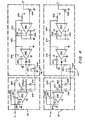
- Band pass filters 18 and 20 are illustrated in FIGURE 3.
- the output of the audio level limiter 16 is provided to the inputs of both filters 18 and 2 0 .
- Band pass filter 18 comprises a series combination of four operational amplifiers 174-180.
- the output of the audio level limiter 16 is supplied through an input resistor 182 in a low pass filter combination of a resistor 184 and a capacitor 186.
- the output of this low pass filter combination is connected to the noninverting input of amplifier 174.
- the inverting input of amplifier 174 is connected to a resistor 188 which is grounded at the opposite terminal.
- Amplifier 174 is equipped with a feedback resistor 190 connecting the output to the inverting input.
- a feedback capacitor 192 connects the output of the amplifier to the input of the low pass filter comprising resistor 184 and capacitor 186.
- Amplifier 174 is also equipped with bypass capacitors 194 and 196 at the power supply terminals.
- Amplifiers 176, 178 and 180 are provided with similar bypass capacitors (not shown).
- the output of amplifier 194 is connected through a load resistor 200 to a low pass filter comprising resistor 202 and capacitor 204.
- the junction of this resistor and capacitor is connected to the noninverting input of the amplifier.
- the inverting input is connected through a resistor 206 to ground.
- a feedback resistor 208 connects the output of amplifier 176 to the inverting input thereof.
- a capacitor 210 is connected between the output of the amplifier and the junction of resistors 200 and 202.
- the output signal from amplifier 176 is connected through a coupling capacitor 212 to a high pass filter comprising capacitor 214 and resistor 216.
- the junction of this capacitor and resistor combination is connected to the noninverting input of resistor 178.
- the noninverting input is connected to one terminal of a resistor 218 which is connected at the opposite terminal to ground.
- Amplifier 178 has a resistor 220 connected between the output and the inverting input and a resistor 222 connected.between the output and the junction of capacitors 212 and 214.
- the output from amplifier 178 is transferred through a coupling capacitor 224 to a high pass filter comprising a capacitor 226 and a resistor 228.
- the junction of capacitor 226 with resistor 228 is connected to the noninverting input of amplifier 180.
- the inverting-input of this amplifier is connected to one terminal of a resistor 230 which is connected at the opposite terminal to ground.
- Amplifier 180 is provided with two feedback resistors. Resistor 232 is connected between-the output of the amplifier and the inverting input while.resistor 234 is connected from the output to the junction of capacitors 224 and 226.
- the output of amplifier 180 is the signal component P 1 which comprises the component of the input audio signal that exist in the frequency band of approximately 25 p to 1100 Hz.
- the high-f.requency band pass filter 20 comprises the series combination of operational amplifiers 240-246.
- the audio signal from level limiter 16 is transmitted through an input resistor 248 to a low pass filter comprising a resistor-250 and a capacitor 252.
- the junction of resistor 250 and 252 is connected to the noninverting input of amplifier 240 while the inverting input is connected to one terminal of a resistor 254 which is connected at the opposite terminal to ground.
- a feedback resistor 256 is connected between the output of amplifier 240 and the inverting input while a feedback capacitor 258 is connected between the output and the junction of resistors 248 and 250.
- Bypass capacitors 260 and 262 are connected respectively to the positive and negative supply terminals of amplifier 240.
- Amplifiers 242, 244 and 246 are equipped with similar bypass capacitors (not shown).
- the output signal from amplifier 240 is connected to an input resistor 264 which is connected in series with a low pass filter comprising resistor 266 and capacitor 268.
- the junction of resistor 266 with the capacitor 268 is connected to the noninverting input of amplifier 242 while the inverting input is connected to one terminal of a resistor 270 which is connected at its opposite terminal to ground.
- Amplifier 242 is provided with two feedback elements.
- a resistor 270 is connected between the output and the inverting input and a capacitor 272 is connected between the output and the junction of resistors 264 and 266.
- the output signal of amplifier 242 is transmitted through a coupling capacitor 274 to a high pass filter comprising capacitor 276 and resistor 278.
- the noninverting input of amplifier 244 is connected to the junction of capacitor 276 with resistor 278.
- the inverting input is connected to one terminal of a resistor 280 which is connected at the opposite terminal to ground.
- Operational amplifier 244 has a feedback resistor 282 connected between the output and the inverting input and a resistor 284 connected between the output and the junction of capacitors 274 and 276.
- the audio signal is transmitted through a coupling capacitor 286 to a high pass filter comprising a capacitor 288 and a resistor 290.
- the noninverting input of amplifier 246 is connected to the junction of capacitor 288 and resistor 290, while the inverting input is connected to one terminal of a resistor 292 which is connected at the opposite terminal to ground.
- a feedback resistor 294 is connected between the output of amplifier 246 and the inverting input while a resistor 296 is connected between the output of amplifier 246 and the junction of capacitors 286 and 288.
- the signal produced at the output of amplifier 246 is P 2 which is the high frequency component of the audio signal supplied by microphone 12.
- the precision rectifiers 24 and 36 together with low pass filters 30 and 42 are shown in FIGURE 4.
- the low frequency audio signal component P 1 is conveyed to a potentiometer 298 which has the opposite terminal grounded.
- the wiper of potentiometer 298 is connected to the noninverting input of an operational amplifier 300.
- the inverting input of amplifier 300 is connected to one terminal of a resistor 302 and the opposite terminal of this resistor is grounded.
- Amplifier 300 is provided with one feedback component, resistor 304 is connected-between the output and the inverting input.
- Amplifier 300 is provided with bypass capacitors 306 and 308 which are connected respectively between the postive and negative.power terminals and ground.
- Amplifier 300 serves as an input buffer for the precision rectifier, the output of the amplifier is transmitted through an input resistor 310 to the inverting input of an operational amplifier 312. The noninverting input of this amplifier is grounded.
- the output of amplifier 312 is connected to a diode 314.
- the rectified signal. at the output of the diode is connected through a feedback resistor 316 to the inverting input of amplifier 312.
- a bypass capacitor 318 is connected to the power supply terminal of amplifier 312.
- the rectified output from diode 314 is also transmitted through a resistor 320 to a potentiometer 322 which has its opposite terminal and the wiper thereof grounded. Potentiometer 322 is provided to adjust the symmetry of the rectification for the incoming audio signal.
- the rectified signal from diode 314 is provided to a series pair of low pass filters which comprise the combination of resistor 324 and capacitor 326 in series with the resistor 328 and capacitor 330.
- the output of these two low pass filters is connected to the noninverting input of an operational amplifier 332.
- the inverting input of amplifier 332 is connected to one terminal of the resistor 334 which is connected at the opposite terminal to ground.
- Amplifier 332 has a parallel combination of resistor 336 and capacitor 338 connected between its output and its inverting input.
- a capacitor 340 is connected to amplifier 332 to provide appropriate frequency limiting.
- a bypass capacitor 342 is connected from the power supply pin of amplifier 332 to ground.
- the low frequency component signal P 1 is input to rectifier 24 where the signal is rectified and then supplied to low pass filter 30 which generates a DC output signal that is proportional to the envelope of the low frequency component signal P 1 .
- the envelope signal for the low frequency component signal P 1 is labeled as A 1 .
- the high frequency component signal P 2 is input to rectifier 36 through a potentiometer 348 which is connected at one terminal to ground.
- the wiper of potentiometer 348 is connected to the noninverting input of an operational amplifier 350.
- This operational amplifier serves as an input buffer for the precision rectifier.
- the inverting input of amplifier 350 is connected to one terminal of a resistor 352 which has the opposite terminal grounded.
- a feedback resistor 354 is connected between the output of amplifier 350 and the inverting input.
- a pair of bypass capacitors 355 and 356 are connected respectively to the postive and negative power supply terminals of amplifier 350.
- the buffered high frequency component signal from the output of amplifier 350 is transmitted through a coupling resistor 358 to the inverting input of an operational amplifier 360.
- the noninverting input of this amplifier is grounded.
- -A bypass capacitor 362 is connected between ground and the postive 15 volt supply terminal of the amplifier 360.
- the output of amplifier 360 is connected through a diode 364 which rectifies the high frequency signal component.
- the output of the diode is connected through a feedback resistor 366 to the inverting input of amplifier 360.
- the diode output is also connected through a resistor 367 to a potentiometer 368 which has the opposite terminal and the wiper thereof grounded. Potentiometer 360 is adjusted to provide rectification symmetry.
- the output of diode 364 is also transmitted to a serial pair of low pass filters comprising resistor 370 and capacitor 372 in series with resistor 374 and capacitor 376.
- the rectified high frequency signal charges capacitors 372 and 376.
- the DC signal on capacitor 376 is connected to the noninverting input of an operational amplifier 378.
- the inverting input of amplifier 378 is connected to one terminal of a resistor 380-which is connected at its opposite terminal to ground.
- Amplifier 378 has a feedback circuit comprising the parallel combination of a resistor 382 and a capacitor 384 connected between the amplifier output and the inverting input.
- a bypass capacitor 386 is connected between ground and the positive 15 volt supply terminal of amplifier 378.
- a bandwidth limiting capacitor 387 is provided with amplifier 378.
- the output signal of amplifier - 378 is the amplitude signal A 2 which is a DC signal proportional to the envelope of high frequency signal component P 2 0
- the low frequency signal component P 1 is also input to the comparator and pulse generator 22 which is shown as a detailed schematic in FIGURE 5.
- the signal P 1 is transmitted through a potentiometer . 392 to the noninverting input of an operational amplifier 394.
- the inverting input of amplifier 394 is grounded.
- a feedback resistor 396 connects the output of amplifier 394 to the noninverting input.
- Bypass capacitors 398 and 400 are connected respectively to the postive and negative voltage supply terminals of amplifier 394.
- the output of amplifier 394 which is biased by a resistor 402 that is connected to a postive 15 volt source, is also connected through a base resistor 404 to a transistor 406.
- a collector resistor 408 connects transistor 406 to the postive 15 volt source.
- the emitter of transistor 406 is grounded while a diode 410 connects the emitter to the base.
- the amplifier 394 together with the transistor 406 generate a pulse at each zero crossover of the signal P 1 . These pulses are generated at the collector terminal of-transistor 406 then input to a dual monostable circuit 410. Circuit 410 generates constant width pulses from the comparator transition pulses provided thereto.
- the high frequency signal component P 2 is supplied to comparator and pulse generator 34 through a potentiometer 412.
- the high frequency signal component is input to the noninverting input of an amplifier 414.
- the inverting input of this amplifier is grounded.
- a feedback resistor 416 connects the output of amplifier 414 to the noninverting input.
- the output of amplifier 414 is biased by a resistor 418 connected to the positive voltage source and is also connected through a base resistor 420 to a transistor 422.
- a collector resistor 424 connects transistor 422 to the postive 15 volt power source.
- the emitter of transistor 422 is grounded while a diode 426 connects the emitter to the base terminals.
- the collector of transistor 422 is connected to pin 11 of the dual monostable circuit 410. As noted above the monostable circuit 410 generates constant width pulses from the comparator transition pulses produced by amplifier 414 and transistor 422.
- the dual monostable circuit 410 is provided with two pulse regulating networks comprising capacitors 428 and 430 connected between pin 2 and ground and pin 14 and ground of the monostable circuit.
- the postive 15 volt power source is connected through a potentiometer 432 and a resistor 434 to pin 2.
- the 15 volt source is likewise connected through a potentiometer 436 and a resistor 438 to pin 14.
- Each of the potentiometers is provided to regulate the pulse width from each half of the dual monostable.
- a bypass capacitorT440 is connected to the 15 volt power terminal of circuit 410.
- the constant width pulses from one half of the monostable circuit 410 are output on pin 6 through a diode 442 to the low pass filter 26, which is shown in FIGURE 1.
- the constant width pulses from diode 442 are input to a low pass frequency network comprising resistor 446 and a capacitor 448.
- a resistor 450 is connected in parallel with capacitor 448 which is grounded.
- the filtered pulse signal from the low pass filter network comprising resistor 446 and capacitor 448 is input to a second low pass filter network comprising a resistor 452 and a capacitor 454. At this point the filtered pulse signal is supplied to the noninverting input of an operational amplifier 456.
- the operational amplifier 456 is provided with a feedback resistor 458 which is connoted between the output terminal and the inverting input terminal.
- Power supply bypass capacitors 460 and 462 are connected respectively to the positive and negative power sources for operational amplifier 456.
- the output signals from amplifier 456 is transmitted through a resistor 464 which is connected to the anode of a diode 466 that is grounded at the cathode terminal.
- the signal present at the junction of resistor 464 and diode 466 is signal F l which is a DC signal proportional to the frequency of the signal component passed through the low frequency channel.
- the monostable circuit 410 generates constant width pulses for the high frequency channel at pin 10.
- a diode-468 is connected to pin 10 in series with a low pass filter network comprising resistor 470 and capacitor 472.
- a resistor 474 is connected in parallel with capacitor 472.
- a second low pass filter network is connected in series with the first low pass filter network and comprises a resistor 476 and a capacitor 478. The output of this second filter network is connected to the noninverting input of an operational amplifier 480.
- a feedback resistor 482 is connected between the output terminal and the inverting input terminal of amplifier 480.
- Bypass capacitors 484 and 486 are connected respectively to the positive and negative voltage supply terminals of amplifier 480.
- the output from amplifier 480 is transmitted through a resistor 488 which is connected to the anode of a diode 490.
- the signal F l is produced at the junction of resistor 488 and diode 490 and comprises a DC signal which is proportional to the frequency of the audio signal component which is passed through the high frequency band pass filter 20.
- Signals F 1 and F 2 are DC level signals which.are proportional to the frequency of the audio component which is passed through the low and high pass filters 18 and 20 respectively.
- the signals A 1 and A2 are also DC level signals but are proportional to the amplitude of the signal envelopes of the audio components which are passed through filters 18 and 20 respectively.
- the input signal is divided into two separate frequency components and the frequency and amplitude of each of these components is converted to a DC signal.
- the remainder of the circuitry shown in FIGURE 6 and 7 provides numerical processing for these signals to generate the output signals which characterize the original audio input signal.
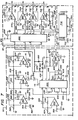
- the signals F 2 , F 1 , A 1 and A 2 are input through resistors 496-502 respectively to an analog switch 504.
- This switch is driven by clock signals derived from timing oscillator 54 so - as to selectively route the input signals to desired output signal lines.
- the timing signals from oscillator 54 are received through lines 506 and 508.
- a bypass capacitor 510 is-connected between the power supply terminal of switch 504 and ground.
- Analog multiplex switch 504 connects on a alternate basis the signals F 1 and F 2 to the scaled product detector 50 and then the signals A 1 and A 2 to the same product detector. This enables one product detector to be used to perform all the multiplication functions necessary in the speech recognition circuit of the present invention. In a like manner the same signals are routed to the scaled ratio detector 52 via lines D x and Dy for analog division operations.
- the signals F 2 and A 1 are alternatively routed through a resistor 512 to a line 514 which is connected to the noninverting input of an operational amplifier 516.
- a feedback resistor 518 is connected between the output of amplifier 516 and the inverting input to control the amplifier gain.
- a bypass capacitor 520 is connected between ground and the postive voltage supply terminal of the operational amplifier 516.
- the output signal from amplifier 516 is connected to pin 10 of an analog multiplier 522.
- the signals F 1 and A 2 are alternatively switched and transmitted through an input resistor 524 to a line 526 which is connected to the noninverting input of an operational amplifier 528.
- the amplifier 528 is provided with a feedback resistor 530 which is connected between the output and the inverting input terminals.
- the output signal from amplifier 528 is connected to pin 9 of the analog multiplier 522.
- the inverting-input terminals of amplifiers 516 and 528 are connected respectively through resistors 532 and 534 to a bias network comprising a potentiometer 536 which is connected at one terminal through a resistor 538 to the negative 15 volt source and at the opposite. terminal through a resistor 540 to ground.
- a capacitor 542 is connected between the wiper terminal of potentiometer 536 and ground.
- the analog multiplier 522 is provided with an external component network for regulating and adjusting the operation of the multiplier operation.
- a resistor 544 is connected between pin terminals 11 and 12 while a resistor 546 is connected between pin terminals 7 and 8.
- a resistor 548 is connected from pin 1 to ground and a capacitor 550 is connected between pin terminals 3 and 5 with terminal 3-being connected to ground and pin 5 being connected to the negative 15 volt power source.
- a bypass capacitor 551 is connected between ground and the positive 15 volt power source which is connected to pin 15.
- a plurality of potentiometers 552, 554 and 556 are connected in parallel between pins 4 and 2. Each of these units is a ten turn potentiometer which provides fine tuning for the multiplication operation.
- the wiper of potentiometer 552 is connected to pin 6, the wiper of potentiometer 554 is connected to pin 13 and the wiper of potentiometer 556 is connected to the noninverting input of an operational amplifier 558.
- the inverting input of amplifier 558 is connected to pin 14 of analog.multiplier 522.
- a feedback network for amplifier 558 connects the output to the input terminal and comprises the parallel combination of a resistor 560 and a capacitor 562.
- a bypass capacitor 564 is connected between the positive 15 volt power source pin of amplifier 558 and ground.
- the output signal from amplifier 558 is transmitted through a resistor.566 to the inverting input of an operational amplifier 568.
- the noninverting input of amplifier 568 is connected to ground.
- a feedback resistor 570 connects the inverting input terminal of amplifier 568 to-the output terminal.
- a bypass capacitor 572 is joined to ground at one terminal and connected to the negative 15 volt power terminal of amplifier 568 at the opposite terminal.
- the output signal from amplifier 568 is transmitted through a resistor 574 which is connected to the anode terminal of a diode 576.
- the cathode terminal of diode 576 is grounded.
- the signal generated at the output of amplifier 568 and transmitted through line 578 is the analog product of the two input signals routed from analog multiplexer 504 to the analog multiplier 522.
- the analog multiplexer 504 also routes two analog signals to the scaled ratio detector 52 shown in FIGURE 7. These two signals are transmitted over lines 514 and 526 to the noninverting inputs respectively of operational amplifiers 580 and 582.
- the signals F 2 and A 1 are alternatively transmitted over line 514 and the signals F 1 and A 2 are alternatively transmitted over line 526.
- a capacitor 584 connects the noninverting input of operational amplifier 580 to ground and a feedback circuit comprising a resistor 586 in parallel with a capacitor 588 is connected between the input and output terminals of the operational amplifier.
- the inverting input of the operational amplifier 580 is connected to a resistor 590 which is grounded.
- Bypass capacitors 592 and 594 are connected respectively to the positive and negative 15 volt power supply pins of amplifier 580.
- the signal produced by amplifier 580 is transmitted through a resistor 596 to the inverting input of an operational amplifier 598.
- the noninverting input of amplifier 598 is grounded.
- a feedback network comprising the parallel combination of a resistor 600 together with a capacitor 602 connects the output terminal of amplifier 598 to the inverting input terminal.
- Bypass capacitors 604 and 606 are connected. between ground and the positive and negative 15 volt supply terminals of amplifier 598.
- the output signal from amplifier 598 is transmitted through a resistor 608 to the inverting input of an operational amplifier 610.
- the input and output terminals of amplifier 610 are interconnected by a feedback network comprising a resistor 610 in parallel with a capacitor 612..
- the noninverting input of amplifier 610 is grounded.
- Bypass capacitor 614 and 616 are connected respectively to the positive and negative 15 volt power supply terminals of amplifier 610.
- the output signal from amplifier 610 is transmitted through a resistor 618 to pin 9 of an analog divider 620.
- Two of the analog signals from analog multiplexer 504 are transmitted over line 526 to the noninverting input of the operational amplifier 582.
- a capacitor 622 connects the noninverting input of amplifier 582 to ground.
- the inverting input is connected to a resistor 624 which is grounded.
- the output terminal and inverting input terminal of operational amplifier 582 are interconnected by a parallel network of a resistor 626 and a capacitor 628.
- the output signal generated by amplifier 582 is connected to pin 10 of analog divider 620.
- An external component network is connected to various terminals of analog divider 620 to provide control and adjustment for the division operation.
- a resistor 630 is connected between terminals 11 and 12, a resistor 632 is connected between terminals 7 and 8 while a resistor 634 is connected between terminals 1 and 3 with terminal 3 being grounded.
- a plurality of potentiometers 636, 638 and 640 are connected in parallel between pins 2 and 4 of analog divider 620.
- the wiper terminal of potentiometer 636 is connected to pin 6, the wiper terminal of potentiometer.638 is connected to pin 13 while the wiper terminal of potentiometer 640 is connected to the noninverting-input of an operational amplifier 642.
- the analog divider 620 is further equipped with a bypass capacitor 644 which is connected between the negative 15 volt power terminal at pin 5 and ground. Another bypass capacitor 646 connects pin 15 which receives the positive 15 volt power source to ground.
- the operational amplifier 642 is provided with a feedback network comprising a resistor 648 in parallel with the capacitor 650, the network being connected between the output terminal of amplifier 642 and the noninverting input terminal thereof.
- a regulating capacitor 648 is connected between selected pin terminals of the integrated circuit comprising amplifier 642.
- bypass capacitors 650 and 652 are connected between ground and the positive and negative 15 volt power terminals of amplifier 642.
- the output signal produced by amplifier 64? is further transmitted through a resistor 654 to the inverting input of amplifier 598.
- the output of the analog divider 620 is transmitted through a line 656 which is connected to pin 9 thereof to a resistor 658 which in connected to two inputs of an analog multiplexer 660.
- a pair of zener diodes 662 and 664 are connected between line 656 and ground to provide voltage regulation. Further, a diode 666 is connected between ground and the two input terminals to analog multiplexer 660 which receive the output of analog divider 620.
- the product signal from analog multiplier 522 is transmitted over line 578 to the remaining two inputs of analog multiplexer 660.
- the four output lines (pins 2, 3, 9 and 10) from multiplexer 660 are selectively connected through output buffers to the input lines 58 to analog to digital converter 60.
- Multiplexer 660 is provided with only one external component, that being a bypass capacitor 668 connected between ground and the positive 15 volt power source.
- the output pins 2, 3, 9 and 10 of analog multiplexer 660 are connected respectively through resistors 670, 672, 674 and 676 to output buffer amplifiers 678, 680, 682 and 684.
- Each of noninverting input terminals of amplifiers 678-684 has a capacitor 686-692 connected respectively to ground.
- Each of the operational amplifiers 678, 680 and 682 has the output terminal thereof connected directly to the inverting input terminal as a feedback line.
- Amplifier 684 has the output thereof connected to the inverting input terminal by the parallel combination of a resistor 694 and a capacitor 696. The inverting input terminal of amplifier 684 is connected to a resistor 698 and the remaining terminal of this resistor is grounded.
- Each of the amplifiers 678-684 has the positive 15 volt power supply terminal connected through a capacitor 700 to ground to bypass any transient components received from the power supply.
- Output resistors 702, 704, 706 and 708 are connected respectively to the output terminals of amplifiers 678, 680, 682 and 684.
- Zener diodes 710, 712, 714 and 716 are connected respectively to the output resistors 702, 704, 706 and 708 to limit the output voltages of the output buffering amplifiers 678, 680, 682 and 684.
- the transmission paths 58 are connected from the buffer amplifiers to the analog to digital conversion unit 60. The product and ratio signals thus produced on these lines are digitized by unit 60 and transmitted for storage and processing through line 62 to computer 64.
- the timing oscillator 54 is connected by lines 506 and 508 to both the analog multiplexer 504 and the analog multiplexer 660.
- Oscillator 54 includes a timing oscillator integrated circuit 718 which is provided with external components comprising a capacitor 722 connected between pins 1 and 3 and a resistor 724 connected between pins 3 and 2.
- a bypass capacitor 726 is connected between pin 14 and ground.
- the circuit of the present invention produces a group of digital words which are representative of an audio sound which is input to microphone 12.
- an operator enters a word or phrase into terminal 70 and the corresponding word or phrase is spoken into microphone 12.
- the audio signal which comprises the word is passed through audio preamp 14 and audio level limiter 16 and is supplied to both the low frequency band pass filter 18 and the high frequency band pass filter 20. Only the respective low and high frequency signal components are passed through the respective filters.
- the low frequency signal component is transmitted to the comparator and pulse generator 22 as well as the precision rectifier 24.
- the high frequency signal component is transnitted simultaneously to the comparator and pulse generator 34 and a precision rectifier 36.
- the zero crossings of the low frequency signal are detected and a pulse is generated for each crossover.
- This pulse train is utilized to drive the monostable circuit 410 to produce a constant width pulse train that varies in frequency with the frequency of the low frequency signal component.
- This variable frequency pulse train is integrated by low pass.filter 26 to produce a DC signal, F 1 , which is proportional to the frequency of the low frequency signal component produced by filter 18.
- the low frequency signal component is also input to precision rectifier 24 and the rectified signal is transmitted to and integrated by low pass filter 30.
- the output of the low pass filter is a signal A l which is a DC signal proportional to the amplitude of the low frequency signal component generated by low frequency band pass filter 18.
- a similar set of operations is carried out for the high frequency signal component of the input audio signal.
- the high frequency signal component, P 2 is input to both the comparator and pulse generator 34 and the precision rectifier 36.
- the comparator and pulse generator 34 a constant width pulse train is produced at the same frequency as the high frequency signal component. This is integrated by low pass filter 38 which produces signal F 2 which is a DC signal proportional to the frequency of the high frequency signal component.
- Signal P 2 is provided to rectifier 36 for rectification and the output is transmitted to low pass filter 42 where it is integrated to produce signal A 2 , the signal A 2 is a DC signal which is proportional to the amplitude of the high frequency signal component, P 2 , which is generated by the high frequency band pass filter 20.
- the four signals F 1 , F 21 A 1 and A 2 are selectively routed through an analog multiplexer 48 to both a scaled product detector 50 and a scaled ratio detector 52.
- the product detector 50 produces two signals. These are M 1 which is the product of the frequency signals F 1 and F 2 and M 2 which is the product of the amplitude signals A 1 and A 2 .
- the scaled ratio detector 52 produces output signals R 1 and R 2 .
- R 1 is the ratio of the frequency signal F 2 to frequency signal F 1 .
- R 2 is the ratio of signal A l to signal A 2 .
- the two product and two ratio signals are inp,ut to the analog multiplexer 56 which selectively connects the signals to the analog to digital converter 60.
- Each of the signals h 1 , M 2 , R l and R 2 are digitized and input to computer 64 via line 62.
- the sequence of digital words produced for each sound is recorded so that it may be correlated with the word or phrase previously input through terminal 70.
- template to represent the spoken word or phrase is described with further reference to FIGURE 8.
- the following described process is carried out for each one of the signals M 1 , M 2 , R 1 and-R 2 .
- Each of these signals is a relational quantity rather than an absolute magnitude or normalized quantity.
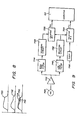
- a relational signal is shown in FIGURE 8 as line 730. This signal is digitized at the sample points shown thereon to produce a digital word representing each of the values of the signal at the-points shown.
- the word or phrase for which the template is to be produced is spoken a number of times, possibly.by different persons in order to produce a template which is sufficiently general to recognize a word despite variations in the pitch and dialect of individual voices.
- line 732 shown in FIGURE 8 is produced-for each spoken word. If the word were spoken in exactly the same manner as in the first instance, line 732 would correspond exactly with line 730. However, due-to the differences between individual speakers and the differences in dialect these lines will not be the same. A comparison of these two lines is shown in the overlay in FIGURE 8.
- the lines 730 and 732 are separated by an area 734 which represent the variance between the two word samples. A plurality of samples are examined and the average value is calculated for each sample point together with the average variance for each sample point. Thus two units of information are recorded for each sample point.
- a template is produced in this manner for each of the four relational signals M 1 , M 2 , R1 and R 2 .
- the group of templates for each word or phrase constitutes a table which corresponds to the particular word or phrase.
- the initial step in carrying out speech recognition with the apparatus of the present invention is to generate a table of templates for each of the words or phrases which will make up the vocabulary for recognition.
- the second major step in speech recognition is to generate a table of templates for an unknown word or phrase and compare the unknown tables to each of the stored tables to find the closest correspondence.
- the word or phrase associated with the table with the closest correspondence is then transferred from the computer to the terminal 70 where.it is displayed to the operator.
- the above steps are repeated for each unknown word so that the text of the input speech is produced as the words are being uttered.
- the apparatus of the present invention can also be utilized to control machinery and production operations. Rather than displaying the identified input speech the computer carries out a set of mechanical operations previously recorded for -the identified word.
- FIGURE 9 An alternative embodiment for a portion of the present invention is illustrated in FIGURE 9.
- the analog method described above for generating the frequency proportional signals F1 and F 2 does not in all cases have the greatest resolution which is needed to insure accurate speech recognition.
- a circuit for producing these two signals with greater accuracy is that shown in FIGURE 9.
- a microphone 740 receives a speech signal which is passed through an amplifier 742 and supplied to a high pass filter 744 and the low pass filter 746. To this point the signal processing is just the same as that described in the above embodiment.
- the high frequency component of the audio signal is transmitted from the output of filter 744 to a squaring circuit 748.
- the output of the squaring circuit is input to a counter 750.
- the low frequency component of the input audio signal is transmitted from low pass filter 746 to a second squaring circuit 752.
- the output of this squaring circuit is input to counter 750 into a second counter 754.
- a clock 756 supplies a time reference signal to counter 754.
- the output of squaring circuit 752 controls the gate of counter 750 so that the output is a count which is the ratio of the frequency of the high frequency component as compared to the frequency of the low frequency component.
- This digital signal corresponds to the analog signal R1.
- the low frequency signal component output of squaring circuit 752 is input as the gate control for counter 754. This operates to count the pulses from the clock 756 with the number of clock pulses from the second counter being proportional to the frequency of the low frequency signal component output by low pass filter 746.
- the output of counter 754 is a digital word which corresponds to the analog signal F 1 .
- the two signal outputs of ⁇ counters 750 and 754 are input to the computer 64.
- the computer 64 then multiples the contents of both counters for an estimate of the frequency of a high frequency signal component.
- the computer then multiplies that product by the output of counter 754 for an estimate of signal M 1 which is the product of the two frequency signals F1 and F 2 .
- the advantage of the embodiment shown in FIGURE 9 over the earlier described analog embodiment is that there is no loss of time resolutions since there is no need to integrate pulses to derive a DC voltage.
- a second advantage is that when a cycle is not detected by the squaring circuit, the previous pulse is carried over into the counter and fed to the computer. This technique eliminates the amount of erroneous data which would be transferred to the computer as a result of poor signal resolution at the end of a speech period.
- the previous embodiments of the present invention have described the production of four relational signals, N 1 , M 2 , R 1 and R 2 .
- the additional relational template is produced in the following manner.
- the high and low frequency signal, F 1 and F 2 are produced in the manner described for either of the above embodiments and are input to a computer and are stored as a series of numbers.
- the computer treats the high and low frequency signal components separately but in the sane fashion.
- the first data point represents the starting frequency in a given word or phrase. This data point is temporarily stored and the second data point is taken and divided by the first.
- the resulting quotient is stored as the first data point in the template.
- the third data point is then taken divided by the first data point and the quotient is stored as the second data point in the template.
- the procedure is continued for the duration of the speech sample.
- the process generates two . additional sets of data for each speech sample and these additional data sets are added to the original tables to represent the dynamic changes in frequency for the two separate frequency bands. These two new sets of frequency data, although derived from the frequency lines, are independent of frequency.
- These two additional relational signals represent the dynamically changing patterns in time which are common to all voices. These additional signals make possible greater resolution of unk:own speech samples while at the same time eliminating spectral variability across speakers because the additional templates are generated by relating the spectrum to itself across frequency and across time. Thus the frequency relationships are stored and analyzed rather than the absolute frequencies themselves.
- relational signals M 1 , M 2 , R 1 . R 2 and the frequency relation across time can be produced by using additional.band pass filters and operating with each additional signal in the manner described above. In certain applications, all of the above described signals may not be required and the desired result may be achieved with use of only one or a few of those relational signals.
- the above invention has been described as an analog processing circuit which generates DC signals that are provided to an analog to digital converter and then to a computer for storage and processing.
- two of the signals are produced by substantially all digital processing with the resulting digital words being fed to the computer which calculates the data point values for the relational signals.
- the input signal can be filtered then digitized and digitally processed in a manner parallel to that described above to produce the same result.
Abstract
Recognition of human speech is carried out by recording a template for each unit of-speech to produce a dictionary of recorded words and phrases. A given speech signal is converted in a similar manner to produce a template which is compared to the stored template to find the closest comparison. The word or phrase corresponding tothe identified template is produced and displayed to complete the recognition of the speech signal. The speech signal is transmitted through low and high pass filters (18, 20) to produce two separate frequency components. The frequency components are input to a comparator impulse generator (22, 34) which generates a pulse train at the rate of the frequency component. The pulse trains is integrated by filters (26, 38) to produce a DC signal proportional to the frequency of the frequency component. The frequency components are also rectified by rectifiers (24, 36) an envelope detector using low pass filters (30, 42) to produce amplitude signals corresponding to the envelope of the frequency components. The products and ratios of the pairs of frequency and amplitude signals are produced to generate a plurality of relational signals which comprise the templates corresponding to each speech signal. The products are produced by a product detector (50) and the ratios are produced by a ratio detector (52). The relational signals are converted from analog to digital format in a converter (60) and then recorded digitally by a computer (64). In building the dictionary each speech sample is submitted a number of times to produce an average template value together with the variants for each data point. The frequency signals are optionally produced by squaring each signal in a squaring circuit (748, 752) and counting the resulting outputs with a gated counter (750) and a timed counter (754). The digital counts thus produced are processed by the computer (64) which calculates the values for each of the frequency signals.
Description
- The field of the invention relates to the electronic recognition of speech and more particularly to a method and apparatus for recognizing speech based on the relational characteristics of signal components comprising the speech signal.
- It has heretofore been realized that speech recognition circuitry coupled with a computer can be used to great advantage in a wide variety of tasks. Typically, the interface between a computer and a human operator has been a mechanical keyboard. A keyboard interface has a number of disadvantages including slow speed, expense, the need for training for the operator and the limitations that the operators hands are fully occupied and cannot be used for other purposes.
- Despite the apparent advantages of speech recognition as an interface between human operators and a computer only limited success has been achieved to date. Numerous obstacles must be overcome before a successful speech recognition system can be implemented at a reasonable cost. A number of problems in designing such a system include the variability of speech from one person to another, the need to produce an accurate template representing each speech unit and the need for a high speed-computer having rapidly accessible mass memory to handle the size of vocabulary needed for a useful application.
- There-exists a need for speech recognition apparatus which is capable of producing speech templates that are essentially independent of the speaker.
- The present invention can be embodied.in a method and apparatus for producing a template to represent an audio signal so that a given audio signal can be compared for example, with a dictionary of scored templates, representing audio signals in order to identify the unknown audio signal. Each of the stored audio signals includes the word or phrase represented by the signal. When the unknown audio signal is identified with a stored signal, the corresponding word or phrase is produced and displayed to the operator. The present invention provides for the recognition of speech for the production of corresponding text.
- More particularly, the present invention provides a method for producing a template to represent an audio signal comprising the steps of extracting a plurality of signal components from the audio signal, producing one or more relational signals each of which is proportional to a plurality of said signal components, and storing the relational signals to serve as the templates which represent each of the audio signals.
- The invention also provides apparatus for producing a template to represent an audio signal comprising:
- means for producing a plurality of signal components derived from said audio signal,
- mathematical operational means connected to receive said signal components for generating proportional relationships for combinations of said signal components to produce one or more relational signals ° each of which is proportional to a plurality of said signal components, and
- means for storing said relational signals to serve as said template which represents said audio signal.
- One way of carrying out the invention will now be described with reference to the accompanying drawings, in which:
- FIGURE 1 is a block diagram of the speech recognition apparatus in accordance with the present invention,
- FIGURE 2 is a circuit diagram of the audio preamplifier and audio level limiter shown in FIGURE 1,
- FIGURE 3 is a circuit diagram of the band pass filters shown in FIGURE 1,
- FIGURE 4 is a circuit diagram of the precision rectifiers and low pass filters shown in FIGURE 1,
- FIGURE 5 is a circuit diagram of the comparators, pulse generator and low pass filters shown in FIGURE 1,
- FIGURE 6 is a circuit diagram of the scaled ratio detectors shown in FIGURE 1,
- FIGURE 7 is a circuit diagram of the ratio detector multiplexing circuit used in FIGURE 1,
- FIGURE 8 is a circuit diagram of the product detectors shown in FIGURE 1,
- FIGURE 9 is an illustration of the process for generating an original word template, and
- FIGURE 10 is a.block diagram for an alternative embodiment of the preprocessing circuitry of the present invention.
- The present invention comprises a method and apparatus for the recognition of human speech. Referring to FIGURE 1, there is shown a block diagram of a first embodiment of the speech recognition apparatus of the present invention. A
speech recognition circuit 10 receives human speech at amicrophone 12 which generates an audio signal that is transferred sequentially through anaudio preamplifier 14 and anaudio level limiter 16. The audio signal generated at the output oflimiter 16 is provided as inputs to a low frequencyband pass filter 18 and a high frequencyband pass filter 20.Filter 18 is designed to have a pass band covering the range of 300 to 1100 Hz.High frequency filter 20 is designed to have a pass band in the range of 1500 to 4500 Hz. The low frequency component P1 of the input audio signal is produced as the output ofband pass filter 18 and the high frequency component P2 of the input audio signal is produced as the output ofband pass filter 20. - The low frequency audio component P1 from
filter 18 is input to both a comparator andpulse generator 22 and aprecision rectifier 24. In the comparator andpulse generator 22 the low frequency component audio signal Pi is zero crossing detected to generate a pulse train corresponding to the frequency of audio signal P1. The pulse train generated bycircuit 22 is passed through alow pass filter 26 which produces a DC voltage F1 on line 28, the signal F1 being proportional to the instantaneous frequency of the audio signal component P1 input to comparator andpulse generator 22. - The low frequency audio signal P1 is rectified in
circuit 24 and the rectified signal is passed through alow pass filter 30 to generate a DC amplitude signal A1 online 32. Signal A1 is proportional to the amplitude of the low frequency audio signal P1 produced at the output offilter 18. - The high frequency audio component P2 received from the
high frequency filter 20 is input to both a comparator andpulse generator 34 and aprecision rectifier 36. Within the comparator andpulse generator 34 the high frequency component signal P2 is zero crossing detected to produce a pulse train corresponding to the frequency of signal P2.. The pulse train is input to alow pass filter 38 to generate a DC signal F2 online 40. Signal F2 is a DC voltage which is proportional to the frequency of the high frequency audio signal component P2. - The high frequency component P2 of the audio signal which is extracted by the
filter 20 is supplied as an input toprecision rectifier 36 and the rectified output thereof is input to alow pass filter 42 to produce a signal A2 online 44, signal A2 being proportional to the amplitude of the high frequency signal P2. - Each of the-DC signals F1, F2, A1 and A2 are input to an
analog multiplexer 48. These analog signals are selectively routed by-multiplexer 48 so that they are provided to a scaledproduct detector 50 and a scaledratio detector 52. The analog signals are routed in a time sequence controlled by clock signals provided by atiming oscillator 54. - The scaled
product detector 50 produces two analog output signals. These are ignals M1 and M2. Signal M1 is proportional to the product of the frequency signals F1 and F2. Signal M2 is proportional to the product of the amplitude signals Al and A2. - The scaled
ratio detector 52 produces signals R1 and R2 where R1 is proportional to the ratio of F2 to F1 and R2 is the ratio of A1 to A27 - In the preferred embodiment of the invention the signals M1, M2, R1 and R2 are defined as follows:


- The constants k1, k2, k3 and k4 are selectable by the operator. The constants k1, k2, k3 and k4 are provided as scaling factors.
- The product signals M1 and M2 from the scaled
product detector 50 are input sequentially to ananalog multiplexer 56. Likewise, the ratio signals R1 and R2 from the scaledratio detector 52 are sequentially input toanalog multiplexer 56. The clock signals generated bytiming oscillator 54 are also provided to multiplexer 56 to provide coordinated sequential operation. The signals provided as inputs toanalog multiplexer 56 are sequentially routed throughline 58 to an analog todigital converter 60. The analog to digital converter 60 samples the analog signals M 1, M2, R1 and R2 as they are provided and produces a digital word corresponding to each of the samples. The digital words are transferred overdata lines 62 to adigital computer 64. The data words are stored indigital computer 64 for further processing or retrieval. The sequence of operations for transferring the analog signals frommultiplexer 56 to analog todigital converter 60 and then the transfer of digital words fromconverter 60 tocomputer 64 is carried out under the control of signals produced bycomputer 64 and transferred overlines - An input/
output terminal 70 is connected tocomputer 64 through abi-directional transmission path 72. An operator can enter information throughterminal 70 to thecomputer 64 and can receive information generated bycomputer 64 and displayed atterminal 70. - The functional blocks described in reference to FIGURE 1 are illustrated in detailed schematic form in FIGURES 2-8. The
audio preamplifier 14 andaudio level limiter 16 are shown in schematic circuit form in FIGURE 2. Themicrophone 12 is connected through aninput connector 82 and the series combination of acapacitor 84 andresistor 86. Aresistor 88 is connected between the junction ofcapacitor 84 andresistor 86 and ground. The audio signal generated bymicrophone 12 is supplied to the noninverting input of anamplifier 90 which serves as a basic audio preamplifier. The noninverting input toamplifier 90 is connected to a series combination ofresistor 92 and acapacitor 94 which is connected at one terminal to ground. - The output of
amplifier 90 is connected to a groundedresistor 100 and through a feedback network to the inverting input of the amplifier. The feedback network comprises the parallel combination of aresistor 102 with acapacitor 104.Bypass capacitors amplifier 90. - The output of
audio preamplifier 14 is input to theaudio level limiter 16 through acoupling capacitor 110 and aninput resistor 112 to anaudio compander 114.Terminals compander 114 are interconnected by a parallel combination ofresistor 116 andcapacitor 118. Acapacitor 120 is connected betweenterminals capacitor 122 couples the output ofaudio compander 114 to theoutput line 124 of the audio preamp circuit. Adischarge resistor 126 is connected between theoutput line 124 and ground. Aresistor 128 is connected betweenpins compander 114 while acapacitor 130 is connected betweenpins Pin 4 ofcompander 114 is grounded. Abypass capacitor 132 is connected betweenpin 13 and ground whilepin 13 is connected to the +15 volt power supply line. - Dual
operational amplifiers input resistor 140 the output ofpin 9 ofcompander 114.Amplifiers compander 114 bias voltages.Amplifier 136 is fitted with afeedback resistor 142 for gain control andamplifier 138 is equipped with asimilar resistor 144. The output ofamplifier 136 is connected to aload resistor 146, apotentiometer 148 and aresistor 150 to the inverting input ofoperational amplifier 138.Potentiometer 148 serves to adjust the limiter threshold. Aresistor 152 is connected between-potentiometer 148 and the +15 volt power terminal. -
Operational.amplifiers amplifier 158 is connected to the wiper ofpotentiometer 148 which receives the output signal ofamplifier 136. The inverting input ofamplifier 160 is connected to directly receive the output ofamplifier 138.Pin 3 ofaudio compander 114 is connected to the inverting input ofamplifier 158 and the noninverting input of 160. The outputs ofamplifiers bias resistor 162 to the +15v. supply and through aresistor 164 to the base of atransistor 166. Acollector resistor 168 connectstransistor 166 to pin 1 ofcompander 114. - The
operational amplifiers bypass capacitors - Band pass filters 18 and 20 are illustrated in FIGURE 3. The output of the
audio level limiter 16 is provided to the inputs of bothfilters Band pass filter 18 comprises a series combination of four operational amplifiers 174-180. The output of theaudio level limiter 16 is supplied through aninput resistor 182 in a low pass filter combination of aresistor 184 and acapacitor 186. The output of this low pass filter combination is connected to the noninverting input ofamplifier 174. The inverting input ofamplifier 174 is connected to aresistor 188 which is grounded at the opposite terminal.Amplifier 174 is equipped with afeedback resistor 190 connecting the output to the inverting input. Afeedback capacitor 192 connects the output of the amplifier to the input of the low passfilter comprising resistor 184 andcapacitor 186.Amplifier 174 is also equipped withbypass capacitors 194 and 196 at the power supply terminals.Amplifiers - The output of amplifier 194 is connected through a
load resistor 200 to a low passfilter comprising resistor 202 andcapacitor 204. The junction of this resistor and capacitor is connected to the noninverting input of the amplifier. The inverting input is connected through aresistor 206 to ground. A feedback resistor 208 connects the output ofamplifier 176 to the inverting input thereof. Acapacitor 210 is connected between the output of the amplifier and the junction ofresistors - The output signal from
amplifier 176 is connected through acoupling capacitor 212 to a high pass filter comprising capacitor 214 andresistor 216. The junction of this capacitor and resistor combination is connected to the noninverting input ofresistor 178. The noninverting input is connected to one terminal of aresistor 218 which is connected at the opposite terminal to ground.Amplifier 178 has aresistor 220 connected between the output and the inverting input and aresistor 222 connected.between the output and the junction ofcapacitors 212 and 214. The output fromamplifier 178 is transferred through acoupling capacitor 224 to a high pass filter comprising acapacitor 226 and aresistor 228. The junction ofcapacitor 226 withresistor 228 is connected to the noninverting input ofamplifier 180. The inverting-input of this amplifier is connected to one terminal of aresistor 230 which is connected at the opposite terminal to ground.Amplifier 180 is provided with two feedback resistors.Resistor 232 is connected between-the output of the amplifier and the invertinginput while.resistor 234 is connected from the output to the junction ofcapacitors amplifier 180 is the signal component P1 which comprises the component of the input audio signal that exist in the frequency band of approximately 25p to 1100 Hz. - The high-f.requency
band pass filter 20 comprises the series combination of operational amplifiers 240-246. The audio signal fromlevel limiter 16 is transmitted through aninput resistor 248 to a low pass filter comprising a resistor-250 and a capacitor 252. The junction ofresistor 250 and 252 is connected to the noninverting input ofamplifier 240 while the inverting input is connected to one terminal of aresistor 254 which is connected at the opposite terminal to ground. Afeedback resistor 256 is connected between the output ofamplifier 240 and the inverting input while afeedback capacitor 258 is connected between the output and the junction ofresistors amplifier 240.Amplifiers - The output signal from
amplifier 240 is connected to aninput resistor 264 which is connected in series with a low passfilter comprising resistor 266 andcapacitor 268. The junction ofresistor 266 with thecapacitor 268 is connected to the noninverting input ofamplifier 242 while the inverting input is connected to one terminal of aresistor 270 which is connected at its opposite terminal to ground.Amplifier 242 is provided with two feedback elements. Aresistor 270 is connected between the output and the inverting input and acapacitor 272 is connected between the output and the junction ofresistors - The output signal of
amplifier 242 is transmitted through acoupling capacitor 274 to a high passfilter comprising capacitor 276 andresistor 278. The noninverting input ofamplifier 244 is connected to the junction ofcapacitor 276 withresistor 278. The inverting input is connected to one terminal of aresistor 280 which is connected at the opposite terminal to ground.Operational amplifier 244 has afeedback resistor 282 connected between the output and the inverting input and aresistor 284 connected between the output and the junction ofcapacitors - From
amplifier 244 the audio signal is transmitted through acoupling capacitor 286 to a high pass filter comprising acapacitor 288 and aresistor 290. The noninverting input ofamplifier 246 is connected to the junction ofcapacitor 288 andresistor 290, while the inverting input is connected to one terminal of aresistor 292 which is connected at the opposite terminal to ground. Afeedback resistor 294 is connected between the output ofamplifier 246 and the inverting input while aresistor 296 is connected between the output ofamplifier 246 and the junction ofcapacitors amplifier 246 is P2 which is the high frequency component of the audio signal supplied bymicrophone 12. - The
precision rectifiers potentiometer 298 which has the opposite terminal grounded. The wiper ofpotentiometer 298 is connected to the noninverting input of anoperational amplifier 300. The inverting input ofamplifier 300 is connected to one terminal of aresistor 302 and the opposite terminal of this resistor is grounded.Amplifier 300 is provided with one feedback component,resistor 304 is connected-between the output and the inverting input.Amplifier 300 is provided withbypass capacitors Amplifier 300 serves as an input buffer for the precision rectifier, the output of the amplifier is transmitted through aninput resistor 310 to the inverting input of anoperational amplifier 312. The noninverting input of this amplifier is grounded. The output ofamplifier 312 is connected to adiode 314. The rectified signal. at the output of the diode is connected through afeedback resistor 316 to the inverting input ofamplifier 312. Abypass capacitor 318 is connected to the power supply terminal ofamplifier 312. The rectified output fromdiode 314 is also transmitted through aresistor 320 to apotentiometer 322 which has its opposite terminal and the wiper thereof grounded.Potentiometer 322 is provided to adjust the symmetry of the rectification for the incoming audio signal. - The rectified signal from
diode 314 is provided to a series pair of low pass filters which comprise the combination ofresistor 324 andcapacitor 326 in series with theresistor 328 andcapacitor 330. The output of these two low pass filters is connected to the noninverting input of anoperational amplifier 332. The inverting input ofamplifier 332 is connected to one terminal of theresistor 334 which is connected at the opposite terminal to ground.Amplifier 332 has a parallel combination ofresistor 336 andcapacitor 338 connected between its output and its inverting input. Acapacitor 340 is connected to amplifier 332 to provide appropriate frequency limiting. Abypass capacitor 342 is connected from the power supply pin ofamplifier 332 to ground. - The low frequency component signal P1 is input to
rectifier 24 where the signal is rectified and then supplied tolow pass filter 30 which generates a DC output signal that is proportional to the envelope of the low frequency component signal P1. The envelope signal for the low frequency component signal P1 is labeled as A1. - The high frequency component signal P2 is input to
rectifier 36 through apotentiometer 348 which is connected at one terminal to ground. The wiper ofpotentiometer 348 is connected to the noninverting input of anoperational amplifier 350. This operational amplifier serves as an input buffer for the precision rectifier. The inverting input ofamplifier 350 is connected to one terminal of aresistor 352 which has the opposite terminal grounded. Afeedback resistor 354 is connected between the output ofamplifier 350 and the inverting input. A pair ofbypass capacitors amplifier 350. - The buffered high frequency component signal from the output of
amplifier 350 is transmitted through acoupling resistor 358 to the inverting input of anoperational amplifier 360. The noninverting input of this amplifier is grounded. -Abypass capacitor 362 is connected between ground and the postive 15 volt supply terminal of theamplifier 360. The output ofamplifier 360 is connected through adiode 364 which rectifies the high frequency signal component. The output of the diode is connected through afeedback resistor 366 to the inverting input ofamplifier 360. The diode output is also connected through aresistor 367 to apotentiometer 368 which has the opposite terminal and the wiper thereof grounded.Potentiometer 360 is adjusted to provide rectification symmetry. - The output of
diode 364 is also transmitted to a serial pair of low pass filters comprising resistor 370 and capacitor 372 in series with resistor 374 andcapacitor 376. The rectified high frequencysignal charges capacitors 372 and 376. The DC signal oncapacitor 376 is connected to the noninverting input of anoperational amplifier 378. The inverting input ofamplifier 378 is connected to one terminal of a resistor 380-which is connected at its opposite terminal to ground.Amplifier 378 has a feedback circuit comprising the parallel combination of aresistor 382 and acapacitor 384 connected between the amplifier output and the inverting input. Abypass capacitor 386 is connected between ground and the positive 15 volt supply terminal ofamplifier 378. Abandwidth limiting capacitor 387 is provided withamplifier 378. The output signal ofamplifier -378 is the amplitude signal A2 which is a DC signal proportional to the envelope of high frequency signal component P20 - The low frequency signal component P1 is also input to the comparator and
pulse generator 22 which is shown as a detailed schematic in FIGURE 5. The signal P1 is transmitted through a potentiometer . 392 to the noninverting input of anoperational amplifier 394. The inverting input ofamplifier 394 is grounded. Afeedback resistor 396 connects the output ofamplifier 394 to the noninverting input.Bypass capacitors amplifier 394. The output ofamplifier 394, which is biased by aresistor 402 that is connected to a postive 15 volt source, is also connected through abase resistor 404 to atransistor 406. Acollector resistor 408 connectstransistor 406 to the postive 15 volt source. The emitter oftransistor 406 is grounded while adiode 410 connects the emitter to the base. Theamplifier 394 together with thetransistor 406 generate a pulse at each zero crossover of the signal P1. These pulses are generated at the collector terminal of-transistor 406 then input to a dualmonostable circuit 410.Circuit 410 generates constant width pulses from the comparator transition pulses provided thereto. - The high frequency signal component P2 is supplied to comparator and
pulse generator 34 through apotentiometer 412. The high frequency signal component is input to the noninverting input of anamplifier 414. The inverting input of this amplifier is grounded. A feedback resistor 416 connects the output ofamplifier 414 to the noninverting input. The output ofamplifier 414 is biased by aresistor 418 connected to the positive voltage source and is also connected through abase resistor 420 to atransistor 422. Acollector resistor 424 connectstransistor 422 to the postive 15 volt power source. The emitter oftransistor 422 is grounded while adiode 426 connects the emitter to the base terminals. The collector oftransistor 422 is connected to pin 11 of the dualmonostable circuit 410. As noted above themonostable circuit 410 generates constant width pulses from the comparator transition pulses produced byamplifier 414 andtransistor 422. - The dual
monostable circuit 410 is provided with two pulse regulatingnetworks comprising capacitors pin 2 and ground andpin 14 and ground of the monostable circuit. The postive 15 volt power source is connected through apotentiometer 432 and aresistor 434 topin 2. The 15 volt source is likewise connected through apotentiometer 436 and aresistor 438 to pin 14. Each of the potentiometers is provided to regulate the pulse width from each half of the dual monostable. A bypass capacitorT440 is connected to the 15 volt power terminal ofcircuit 410. - The constant width pulses from one half of the
monostable circuit 410 are output onpin 6 through adiode 442 to thelow pass filter 26, which is shown in FIGURE 1. The constant width pulses fromdiode 442 are input to a low pass frequencynetwork comprising resistor 446 and acapacitor 448. Aresistor 450 is connected in parallel withcapacitor 448 which is grounded. The filtered pulse signal from the low pass filternetwork comprising resistor 446 andcapacitor 448 is input to a second low pass filter network comprising aresistor 452 and acapacitor 454. At this point the filtered pulse signal is supplied to the noninverting input of anoperational amplifier 456. Due to the filtering of the low pass networks and-the high input impedance ofamplifier 456 the pulse signal at the input terminal of the amplifier has been converted into a DC level signal which is proportional to the pulse rate.. Theoperational amplifier 456 is provided with afeedback resistor 458 which is connoted between the output terminal and the inverting input terminal. Powersupply bypass capacitors operational amplifier 456. The output signals fromamplifier 456 is transmitted through a resistor 464 which is connected to the anode of adiode 466 that is grounded at the cathode terminal. The signal present at the junction of resistor 464 anddiode 466 is signal Fl which is a DC signal proportional to the frequency of the signal component passed through the low frequency channel. - The
monostable circuit 410 generates constant width pulses for the high frequency channel atpin 10. A diode-468 is connected to pin 10 in series with a low pass filter network comprising resistor 470 andcapacitor 472. Aresistor 474 is connected in parallel withcapacitor 472. A second low pass filter network is connected in series with the first low pass filter network and comprises aresistor 476 and acapacitor 478. The output of this second filter network is connected to the noninverting input of anoperational amplifier 480. Afeedback resistor 482 is connected between the output terminal and the inverting input terminal ofamplifier 480.Bypass capacitors amplifier 480. The output fromamplifier 480 is transmitted through a resistor 488 which is connected to the anode of adiode 490. The signal Fl is produced at the junction of resistor 488 anddiode 490 and comprises a DC signal which is proportional to the frequency of the audio signal component which is passed through the high frequencyband pass filter 20. - As described to this point the circuit has produced four signals which are functions of the audio signal provided to the input of the
voice recognition equipment 10 throughmicrophone 12. Signals F1 and F2 are DC level signals which.are proportional to the frequency of the audio component which is passed through the low and high pass filters 18 and 20 respectively. The signals A1 and A2 are also DC level signals but are proportional to the amplitude of the signal envelopes of the audio components which are passed throughfilters - Referring to FIGURE 6 the signals F2, F1, A1 and A2 are input through resistors 496-502 respectively to an
analog switch 504. This switch is driven by clock signals derived from timingoscillator 54 so - as to selectively route the input signals to desired output signal lines. The timing signals fromoscillator 54 are received throughlines switch 504 and ground. -
Analog multiplex switch 504 connects on a alternate basis the signals F1 and F2 to the scaledproduct detector 50 and then the signals A1 and A2 to the same product detector. This enables one product detector to be used to perform all the multiplication functions necessary in the speech recognition circuit of the present invention. In a like manner the same signals are routed to the scaledratio detector 52 via lines Dx and Dy for analog division operations. - The signals F2 and A1 are alternatively routed through a
resistor 512 to aline 514 which is connected to the noninverting input of anoperational amplifier 516. Afeedback resistor 518 is connected between the output ofamplifier 516 and the inverting input to control the amplifier gain. Abypass capacitor 520 is connected between ground and the postive voltage supply terminal of theoperational amplifier 516. The output signal fromamplifier 516 is connected to pin 10 of ananalog multiplier 522. - The signals F1 and A2 are alternatively switched and transmitted through an
input resistor 524 to aline 526 which is connected to the noninverting input of anoperational amplifier 528. Theamplifier 528 is provided with afeedback resistor 530 which is connected between the output and the inverting input terminals. The output signal fromamplifier 528 is connected to pin 9 of theanalog multiplier 522. - The inverting-input terminals of
amplifiers resistors potentiometer 536 which is connected at one terminal through aresistor 538 to the negative 15 volt source and at the opposite. terminal through aresistor 540 to ground. A capacitor 542 is connected between the wiper terminal ofpotentiometer 536 and ground. - The
analog multiplier 522 is provided with an external component network for regulating and adjusting the operation of the multiplier operation. Aresistor 544 is connected betweenpin terminals pin terminals resistor 548 is connected frompin 1 to ground and acapacitor 550 is connected betweenpin terminals pin 5 being connected to the negative 15 volt power source. Abypass capacitor 551 is connected between ground and the positive 15 volt power source which is connected to pin 15. A plurality ofpotentiometers pins potentiometer 552 is connected to pin 6, the wiper ofpotentiometer 554 is connected to pin 13 and the wiper ofpotentiometer 556 is connected to the noninverting input of anoperational amplifier 558. The inverting input ofamplifier 558 is connected to pin 14 ofanalog.multiplier 522. A feedback network foramplifier 558 connects the output to the input terminal and comprises the parallel combination of aresistor 560 and acapacitor 562. Abypass capacitor 564 is connected between the positive 15 volt power source pin ofamplifier 558 and ground. - The output signal from
amplifier 558 is transmitted through a resistor.566 to the inverting input of anoperational amplifier 568. The noninverting input ofamplifier 568 is connected to ground. Afeedback resistor 570 connects the inverting input terminal ofamplifier 568 to-the output terminal..A bypass capacitor 572 is joined to ground at one terminal and connected to the negative 15 volt power terminal ofamplifier 568 at the opposite terminal. The output signal fromamplifier 568 is transmitted through aresistor 574 which is connected to the anode terminal of adiode 576. The cathode terminal ofdiode 576 is grounded. The signal generated at the output ofamplifier 568 and transmitted throughline 578 is the analog product of the two input signals routed fromanalog multiplexer 504 to theanalog multiplier 522. - The
analog multiplexer 504 also routes two analog signals to the scaledratio detector 52 shown in FIGURE 7. These two signals are transmitted overlines operational amplifiers line 514 and the signals F1 and A2 are alternatively transmitted overline 526. Acapacitor 584 connects the noninverting input ofoperational amplifier 580 to ground and a feedback circuit comprising aresistor 586 in parallel with acapacitor 588 is connected between the input and output terminals of the operational amplifier. The inverting input of theoperational amplifier 580 is connected to aresistor 590 which is grounded.Bypass capacitors amplifier 580. - The signal produced by
amplifier 580 is transmitted through aresistor 596 to the inverting input of anoperational amplifier 598. The noninverting input ofamplifier 598 is grounded. A feedback network comprising the parallel combination of aresistor 600 together with acapacitor 602 connects the output terminal ofamplifier 598 to the inverting input terminal.Bypass capacitors amplifier 598. - The output signal from
amplifier 598 is transmitted through aresistor 608 to the inverting input of anoperational amplifier 610. The input and output terminals ofamplifier 610 are interconnected by a feedback network comprising aresistor 610 in parallel with acapacitor 612.. The noninverting input ofamplifier 610 is grounded.Bypass capacitor 614 and 616 are connected respectively to the positive and negative 15 volt power supply terminals ofamplifier 610. The output signal fromamplifier 610 is transmitted through a resistor 618 to pin 9 of ananalog divider 620. - Two of the analog signals from
analog multiplexer 504 are transmitted overline 526 to the noninverting input of theoperational amplifier 582. Acapacitor 622 connects the noninverting input ofamplifier 582 to ground. The inverting input is connected to aresistor 624 which is grounded. The output terminal and inverting input terminal ofoperational amplifier 582 are interconnected by a parallel network of aresistor 626 and acapacitor 628. The output signal generated byamplifier 582 is connected to pin 10 ofanalog divider 620. - An external component network is connected to various terminals of
analog divider 620 to provide control and adjustment for the division operation. Aresistor 630 is connected betweenterminals resistor 632 is connected betweenterminals resistor 634 is connected betweenterminals terminal 3 being grounded. A plurality ofpotentiometers pins analog divider 620. The wiper terminal ofpotentiometer 636 is connected to pin 6, the wiper terminal of potentiometer.638 is connected to pin 13 while the wiper terminal ofpotentiometer 640 is connected to the noninverting-input of anoperational amplifier 642. Theanalog divider 620 is further equipped with a bypass capacitor 644 which is connected between the negative 15 volt power terminal atpin 5 and ground. Anotherbypass capacitor 646 connectspin 15 which receives the positive 15 volt power source to ground. - The
operational amplifier 642 is provided with a feedback network comprising aresistor 648 in parallel with thecapacitor 650, the network being connected between the output terminal ofamplifier 642 and the noninverting input terminal thereof. A regulatingcapacitor 648 is connected between selected pin terminals of the integratedcircuit comprising amplifier 642. Inaddition bypass capacitors amplifier 642. The output signal produced byamplifier 64? is further transmitted through aresistor 654 to the inverting input ofamplifier 598. - The output of the
analog divider 620 is transmitted through aline 656 which is connected to pin 9 thereof to aresistor 658 which in connected to two inputs of ananalog multiplexer 660. A pair ofzener diodes line 656 and ground to provide voltage regulation. Further, adiode 666 is connected between ground and the two input terminals toanalog multiplexer 660 which receive the output ofanalog divider 620. The product signal fromanalog multiplier 522 is transmitted overline 578 to the remaining two inputs ofanalog multiplexer 660. The four output lines (pins 2, 3, 9 and 10) frommultiplexer 660 are selectively connected through output buffers to the input lines 58 to analog todigital converter 60.Multiplexer 660 is provided with only one external component, that being abypass capacitor 668 connected between ground and the positive 15 volt power source. - The output pins 2, 3, 9 and 10 of
analog multiplexer 660 are connected respectively throughresistors output buffer amplifiers - Each of the
operational amplifiers Amplifier 684 has the output thereof connected to the inverting input terminal by the parallel combination of aresistor 694 and acapacitor 696. The inverting input terminal ofamplifier 684 is connected to aresistor 698 and the remaining terminal of this resistor is grounded. Each of the amplifiers 678-684 has the positive 15 volt power supply terminal connected through acapacitor 700 to ground to bypass any transient components received from the power supply.Output resistors amplifiers Zener diodes output resistors output buffering amplifiers transmission paths 58 are connected from the buffer amplifiers to the analog todigital conversion unit 60. The product and ratio signals thus produced on these lines are digitized byunit 60 and transmitted for storage and processing throughline 62 tocomputer 64. - The
timing oscillator 54 is connected bylines analog multiplexer 504 and theanalog multiplexer 660.Oscillator 54 includes a timing oscillator integratedcircuit 718 which is provided with external components comprising acapacitor 722 connected betweenpins resistor 724 connected betweenpins bypass capacitor 726 is connected betweenpin 14 and ground. - The part numbers and the manufacturers for the various integrated circuits utilized in the present invention are listed in the following component table.

- The overall operation of the present speech recognition apparatus is given in reference to FIGURES 1-7. The circuit of the present invention produces a group of digital words which are representative of an audio sound which is input to
microphone 12. In practice an operator enters a word or phrase intoterminal 70 and the corresponding word or phrase is spoken intomicrophone 12. The audio signal which comprises the word is passed throughaudio preamp 14 andaudio level limiter 16 and is supplied to both the low frequencyband pass filter 18 and the high frequencyband pass filter 20. Only the respective low and high frequency signal components are passed through the respective filters. The low frequency signal component is transmitted to the comparator andpulse generator 22 as well as theprecision rectifier 24. The high frequency signal component is transnitted simultaneously to the comparator andpulse generator 34 and aprecision rectifier 36. - In the comparator and
pulse generator 22, shown in detail in FIGURE 5, the zero crossings of the low frequency signal are detected and a pulse is generated for each crossover. This pulse train is utilized to drive themonostable circuit 410 to produce a constant width pulse train that varies in frequency with the frequency of the low frequency signal component. This variable frequency pulse train is integrated bylow pass.filter 26 to produce a DC signal, F1, which is proportional to the frequency of the low frequency signal component produced byfilter 18. - The low frequency signal component is also input to
precision rectifier 24 and the rectified signal is transmitted to and integrated bylow pass filter 30. The output of the low pass filter is a signal Al which is a DC signal proportional to the amplitude of the low frequency signal component generated by low frequencyband pass filter 18. - A similar set of operations is carried out for the high frequency signal component of the input audio signal. The high frequency signal component, P2, is input to both the comparator and
pulse generator 34 and theprecision rectifier 36. In the comparator and pulse generator 34 a constant width pulse train is produced at the same frequency as the high frequency signal component. This is integrated bylow pass filter 38 which produces signal F2 which is a DC signal proportional to the frequency of the high frequency signal component. - Signal P2 is provided to
rectifier 36 for rectification and the output is transmitted tolow pass filter 42 where it is integrated to produce signal A2, the signal A2 is a DC signal which is proportional to the amplitude of the high frequency signal component, P2, which is generated by the high frequencyband pass filter 20. - The four signals F1, F21 A1 and A2 are selectively routed through an
analog multiplexer 48 to both a scaledproduct detector 50 and a scaledratio detector 52. Theproduct detector 50 produces two signals. These are M1 which is the product of the frequency signals F1 and F2 and M2 which is the product of the amplitude signals A1 and A2. The scaledratio detector 52 produces output signals R1 and R2. R1 is the ratio of the frequency signal F2 to frequency signal F1. R2 is the ratio of signal Al to signal A2. The two product and two ratio signals are inp,ut to theanalog multiplexer 56 which selectively connects the signals to the analog todigital converter 60. Each of the signals h1, M2, Rl and R2 are digitized and input tocomputer 64 vialine 62. The sequence of digital words produced for each sound is recorded so that it may be correlated with the word or phrase previously input throughterminal 70. - The production of template to represent the spoken word or phrase is described with further reference to FIGURE 8. The following described process is carried out for each one of the signals M1, M2, R1 and-R2. Each of these signals is a relational quantity rather than an absolute magnitude or normalized quantity. A relational signal is shown in FIGURE 8 as
line 730. This signal is digitized at the sample points shown thereon to produce a digital word representing each of the values of the signal at the-points shown. In the preferred method of the present invention the word or phrase for which the template is to be produced is spoken a number of times, possibly.by different persons in order to produce a template which is sufficiently general to recognize a word despite variations in the pitch and dialect of individual voices. As the word is spoken the second and succeeding times the identical processing of the signal is carried out and a new line, such asline 732 shown in FIGURE 8 is produced-for each spoken word. If the word were spoken in exactly the same manner as in the first instance,line 732 would correspond exactly withline 730. However, due-to the differences between individual speakers and the differences in dialect these lines will not be the same. A comparison of these two lines is shown in the overlay in FIGURE 8. Thelines area 734 which represent the variance between the two word samples. A plurality of samples are examined and the average value is calculated for each sample point together with the average variance for each sample point. Thus two units of information are recorded for each sample point. A template is produced in this manner for each of the four relational signals M1, M2, R1 and R2. The group of templates for each word or phrase constitutes a table which corresponds to the particular word or phrase. - The initial step in carrying out speech recognition with the apparatus of the present invention is to generate a table of templates for each of the words or phrases which will make up the vocabulary for recognition. The second major step in speech recognition is to generate a table of templates for an unknown word or phrase and compare the unknown tables to each of the stored tables to find the closest correspondence. The word or phrase associated with the table with the closest correspondence is then transferred from the computer to the terminal 70 where.it is displayed to the operator. The above steps are repeated for each unknown word so that the text of the input speech is produced as the words are being uttered.
- The apparatus of the present invention can also be utilized to control machinery and production operations. Rather than displaying the identified input speech the computer carries out a set of mechanical operations previously recorded for -the identified word.
- An alternative embodiment for a portion of the present invention is illustrated in FIGURE 9. The analog method described above for generating the frequency proportional signals F1 and F2 does not in all cases have the greatest resolution which is needed to insure accurate speech recognition. A circuit for producing these two signals with greater accuracy is that shown in FIGURE 9. A
microphone 740 receives a speech signal which is passed through anamplifier 742 and supplied to ahigh pass filter 744 and thelow pass filter 746. To this point the signal processing is just the same as that described in the above embodiment. The high frequency component of the audio signal is transmitted from the output offilter 744 to asquaring circuit 748. The output of the squaring circuit is input to acounter 750. - The low frequency component of the input audio signal is transmitted from
low pass filter 746 to asecond squaring circuit 752. The output of this squaring circuit is input to counter 750 into asecond counter 754. Aclock 756 supplies a time reference signal to counter 754. - The output of squaring
circuit 752 controls the gate ofcounter 750 so that the output is a count which is the ratio of the frequency of the high frequency component as compared to the frequency of the low frequency component. This digital signal corresponds to the analog signal R1. The low frequency signal component output of squaringcircuit 752 is input as the gate control forcounter 754. This operates to count the pulses from theclock 756 with the number of clock pulses from the second counter being proportional to the frequency of the low frequency signal component output bylow pass filter 746. The output ofcounter 754 is a digital word which corresponds to the analog signal F1. The two signal outputs of ω counters 750 and 754 are input to thecomputer 64. Thecomputer 64 then multiples the contents of both counters for an estimate of the frequency of a high frequency signal component. The computer then multiplies that product by the output ofcounter 754 for an estimate of signal M1 which is the product of the two frequency signals F1 and F2. - The advantage of the embodiment shown in FIGURE 9 over the earlier described analog embodiment is that there is no loss of time resolutions since there is no need to integrate pulses to derive a DC voltage. A second advantage is that when a cycle is not detected by the squaring circuit, the previous pulse is carried over into the counter and fed to the computer. This technique eliminates the amount of erroneous data which would be transferred to the computer as a result of poor signal resolution at the end of a speech period.
- The previous embodiments of the present invention have described the production of four relational signals, N1, M2, R1 and R2. There is a still further relational signal which can be produced and included in the template previously described to assist in the recognition of speech. The additional relational template is produced in the following manner. The high and low frequency signal, F1 and F2 are produced in the manner described for either of the above embodiments and are input to a computer and are stored as a series of numbers. The computer treats the high and low frequency signal components separately but in the sane fashion. The first data point represents the starting frequency in a given word or phrase. This data point is temporarily stored and the second data point is taken and divided by the first. The resulting quotient is stored as the first data point in the template. The third data point is then taken divided by the first data point and the quotient is stored as the second data point in the template. The procedure is continued for the duration of the speech sample. The process generates two . additional sets of data for each speech sample and these additional data sets are added to the original tables to represent the dynamic changes in frequency for the two separate frequency bands. These two new sets of frequency data, although derived from the frequency lines, are independent of frequency. These two additional relational signals represent the dynamically changing patterns in time which are common to all voices. These additional signals make possible greater resolution of unk:own speech samples while at the same time eliminating spectral variability across speakers because the additional templates are generated by relating the spectrum to itself across frequency and across time. Thus the frequency relationships are stored and analyzed rather than the absolute frequencies themselves.
- Speech recognition has been described for the present invention using relational signals M1, M2, R1. R2 and the frequency relation across time. Further relational signals can be produced by using additional.band pass filters and operating with each additional signal in the manner described above. In certain applications, all of the above described signals may not be required and the desired result may be achieved with use of only one or a few of those relational signals.
- The above invention has been described as an analog processing circuit which generates DC signals that are provided to an analog to digital converter and then to a computer for storage and processing. In a further embodiment, two of the signals are produced by substantially all digital processing with the resulting digital words being fed to the computer which calculates the data point values for the relational signals. In a still further embodiment of the present invention, the input signal can be filtered then digitized and digitally processed in a manner parallel to that described above to produce the same result. Although several embodiments of the invention have been illustrated in the accompanying drawings and described in the. foregoing detailed description, it will be understood that the invention is not limited to the embodiments disclosed, but is capable of numerous rearrangements, modifications and substitutions without departing from the scope of the invention.
Claims (21)
1. A method for producing a template to represent an audio signal, comprising the steps of:
extracting a plurality of signal components from said audio signal,
producing one or more relational signals'each of which is proportional to a plurality of said signal components, and
storing said relational signals to serve as said template which represents said audio signal.
2. A method-according to Claim 1 wherein the step of extracting a plurality of signal components comprises:
filtering said audio signal through filters, each of which passes a different spectral region of said audio signal,
producing a frequency signal for each signal produced at the output of said filters, each said frequency signal proportional to the frequency of the output signal from the respective filter, and
producing an amplitude signal for each of said signals produced at the output of said filters, each said amplitude signal proportional to the envelope of the output signal from the respective filter.
3. A method according to Claim 2 wherein the step of generating one or more relational signals comprises:
producing a frequency product signal which is proportional to the product of said frequency signals,
producing a frequency ratio signal which is proportional to the ratio of said frequency signals,
producing an amplitude product signal which is proportional to the product of said amplitude signals, and
producing an amplitude ratio signal which is proportional to the ratio of said amplitude signals.
4. A method according to Claim 1 wherein the step of generating one or more relational signals comprises:
producing a first relational signal which is the product of two of said signal components, and
producing a second relational signal which is the ratio of two of said signal components.
5. A method according to Claim 3 wherein the step of producing a frequency signal comprises detecting the zero crossovers of said frequency component signals, producing a pulse for each detected crossover and filtering said pulses to produce said frequency signals.
6. A method according to Claim 3 wherein the step of producing an amplitude signal comprises envelope detecting each of said frequency component signals to produce said amplitude signals.
7. A method according to Claim 1 wherein the extracted signal components are spectral component signals of said audio signal, said extracting step including quantizing said spectral component signals into sequential units, and wherein said relational signals are produced-corresponding to each spectral component signal wherein the relational signal comprises a sequence of data points, each data point comprising the ratio of corresponding sequential unit in serial order to the first sequential unit, said relational signals comprising said templates.
8. A method according to Claim 7 wherein the step of quantizing said spectral component signals comprises digitizing said spectral component signals to produce digital words representing each sequential unit.
9. A method according to Claim 8 wherein the step of producing a relational signal comprises sequentially dividing each of said digital word making up a spectral component signal by the first of said digital words, said relational signal comprising the resulting sequence of digitized words.
10. A method according to Claim 1, 2 or 3 which is carried out for producing a generalized template representing a speech pattern signal which is repeated a number of times comprising the steps of:
extracting a plurality of signal components from each said speech pattern signal,
generating one or more relational signals for each said speech pattern, each of said relational signals proportional to a plurality of said signal components derived from one of said speech pattern signals,
averaging the corresponding relational signals of said speech pattern signals to produce an average relational signal,
measuring the deviation of said relational signals from said average relational signal to produce a deviation signal for each of said relational signals, and
storing each of said average relational signals and the corresponding deviation signals.
11. A method according to any one of Claims 1, 2 or 3 wherein the extracted signal components are at least two frequency component signals of said audio signal and including-the steps of:-
providing a first of said frequency component signals to the input terminal of a gated counter,
providing a second of said frequency component signals to the gate terminal of said counter to cause the first frequency component signal to be counted when the gate of the counter is activated by said second frequency component signal, the first frequency component signal count thus produced being proportional to the ratio of the frequency of first frequency component signal to the frequency of the second frequency component signal,
counting the second frequency component signal to produce a second frequency signal proportional to the frequency of the second frequency component signal,
producing a first frequency signal proportional to the frequency of said first frequency component signal by multiplying said first frequency component signal count by said second frequency signal, and
producing an amplitude signal from each of said frequency component signals, said amplitude signals proportional to the envelopes of the respective frequency -component signal,
said relational signals being produced such that each is proportional to a plurality of signals selected from said frequency signals and said amplitude signals.
12. A method according to any one of the preceding claims including the step of digitizing said relational signals before storing.
13. A method according to any one of the preceding claims including the steps of:-
comparing the relational signal template of said given speech signal with the templates representing a dictionary of speech signals to find the closest comparison, and
identifying the given speech signal with the closest comparison stored speech signal.
14. A method according to Claim 13 including the steps of:-
storing the words represented by each of said speech signals included in said dictionary, and
displaying the word represented by the identified speech signal from said dictionary, the displayed word corresponding to the given speech signal.
15. A method according to Claim 13 wherein the steps of extracting a plurality of signal components and producing one or more relational signals are carried out for each of a plurality of utterances for each speech signal in said dictionary, the utterances for each speech signal not identical, averaging said relational signals to produce said templates, recording the deviations of said relational signals for said utterances for said averaged relational signals, and utilizing said deviations to determine the closest comparison of the template for said given signal to the temples in said library.
16. Apparatus for producing a template to represent an audio signal comprising:-
means for producing a plurality of signal components derived from said audio signal,
mathematical operational means connected to receive said signal-components for generating proportional relationships for combinations of said signal components to produce one or more relational signals each of which is proportional to a plurality of said signal components, and
means for storing said relational signals to serve as said template which represents said audio signal.
17. Apparatus according to Claim 16 wherein said means for producing a plurality of signal components comprises:
filter means for filtering said audio signal to produce a plurality of output signals, each output signal corresponding to a different spectral region of said audio signal,
means for detecting the zero crossings for each of said output signals and generating a pulse.train with a pulse occurring at each of said zero crossovers,
means for converting said pulse trains into frequency signals each of which is proportional to the frequency of one of said output signals, and
means for envelope detecting each of said output signals to produce an amplitude signal corresponding to each of said output signals.
18. Apparatus according to claim 16 or 17 wherein said mathematical operational means comprises:
multiplication means connected to receive said frequency signals and said amplitude signals for producing a frequency product signal which is the product of said frequency signals and for producing an amplitude product signal which is the product of said amplitude signals, and
division-means converted to receive said frequency signals and said amplitude signals for producing a frequency ratio signal which is the ratio of one of said frequency signals to another of said frequency signals and for producing an amplitude ratio signal which is the ratio of one of said amplitude signals to another of said amplitude signals, said product and said ratio signals comprising said relational signals.
19. Apparatus according to Claim 16 wherein the means for producing a plurality of signal components comprises:
filter means connected to receive said audio signal for passing a first frequency component thereof,
filter means connected to receive said audio signal for passing a second frequency component thereof, said first component being higher than said second component,
means connected to receive said frequency components for producing a frequency signal for each frequency component, each said frequency signal proportional to the predominant frequency of the corresponding frequency component,
means connected to receive said first frequency component for producing an amplitude signal corresponding to the envelope of said first frequency component,
means connected to receive said second frequency component for producing an amplitude signal corresponding to the envelope of said second frequency signal,
and wherein the mathematical operational means comprises:-
multiplication means connected to receive said frequency and said amplitude signals for producing a frequency product signal which is proportional to the product of said frequency signals and for producing an amplitude product signal which is proportional to the product of said amplitude signals, and
division means connected to receive said frequency and amplitude signals for producing a frequency ratio signal which is proportional to the ratio of one of said frequency signals to another of said frequency signals and for producing an amplitude ratio signal which is proportional to the ratio of one of said amplitude signals-to another of said amplitude signals, said product and ratio signals being stored to serve as said template to represent said audio signal.
20. Apparatus according to Claim 19 wherein said means connected to receive said frequency components for producing a frequency signal for each frequency component comprises:-
means for detecting the zero crossings of each of said frequency components,
means for generating a pulse for each of said detected zero crossings to produce a pulse train for each of said frequency components, and
means for integrating each of said pulse trains to produce said frequency signals.
21. Apparatus according to Claim 19 wherein said means connected to receive said frequency components for producing a frequency signal for each frequency component comprises:-
a first squaring circuit connected to receive said high frequency component and produce a pulsed signal corresponding in frequency to said high frequency component,
a second squaring circuit connected to receive said low frequency component and produce a pulsed signal corresponding in frequency to said low frequency component,
a gated counter connected to receive and count said pulsed signal from said first squaring circuit, the gate of said counter connected to be operated by said pulsed signal from said received squaring circuit, said gated counter producing a digitized signal proportional to the ratio of said frequency signals,
a clocked-counter connected to receive and count said pulsed signal from said second squaring circuit, said clocked counter producing a digitized signal proportional to the frequency of said low frequency signal, and
means for multiplying said digitized ratio signal by said digitized frequency signal to produce a digitized signal proportional to said high frequency component.
Applications Claiming Priority (2)
| Application Number | Priority Date | Filing Date | Title |
|---|---|---|---|
| US06/114,724 US4383135A (en) | 1980-01-23 | 1980-01-23 | Method and apparatus for speech recognition |
| US114724 | 1980-01-23 |
Publications (2)
| Publication Number | Publication Date |
|---|---|
| EP0033412A2 true EP0033412A2 (en) | 1981-08-12 |
| EP0033412A3 EP0033412A3 (en) | 1981-10-14 |
Family
ID=22357054
Family Applications (1)
| Application Number | Title | Priority Date | Filing Date |
|---|---|---|---|
| EP80303965A Ceased EP0033412A3 (en) | 1980-01-23 | 1980-11-06 | Method and apparatus for speech recognition |
Country Status (3)
| Country | Link |
|---|---|
| US (1) | US4383135A (en) |
| EP (1) | EP0033412A3 (en) |
| JP (2) | JPS56109400A (en) |
Cited By (8)
| Publication number | Priority date | Publication date | Assignee | Title |
|---|---|---|---|---|
| US4759068A (en) * | 1985-05-29 | 1988-07-19 | International Business Machines Corporation | Constructing Markov models of words from multiple utterances |
| US4827521A (en) * | 1986-03-27 | 1989-05-02 | International Business Machines Corporation | Training of markov models used in a speech recognition system |
| EP0336032A1 (en) * | 1988-04-07 | 1989-10-11 | Research Triangle Institute | Audio visual speech recognition |
| US4882759A (en) * | 1986-04-18 | 1989-11-21 | International Business Machines Corporation | Synthesizing word baseforms used in speech recognition |
| US4980826A (en) * | 1983-11-03 | 1990-12-25 | World Energy Exchange Corporation | Voice actuated automated futures trading exchange |
| EP0411290A2 (en) * | 1989-08-04 | 1991-02-06 | Scott Instruments Corporation | Method and apparatus for extracting information-bearing portions of a signal for recognizing varying instances of similar patterns |
| EP0508547A2 (en) * | 1991-04-12 | 1992-10-14 | Philips Patentverwaltung GmbH | Circuit for speech recognition |
| CN104851424A (en) * | 2015-04-06 | 2015-08-19 | 何涛 | Voice recognition caring and nursing method and system |
Families Citing this family (22)
| Publication number | Priority date | Publication date | Assignee | Title |
|---|---|---|---|---|
| US5165007A (en) * | 1985-02-01 | 1992-11-17 | International Business Machines Corporation | Feneme-based Markov models for words |
| US4797927A (en) * | 1985-10-30 | 1989-01-10 | Grumman Aerospace Corporation | Voice recognition process utilizing content addressable memory |
| US4891602A (en) * | 1987-01-07 | 1990-01-02 | Bernard Strehler | Visual/voice input recognition sensor |
| US4980917A (en) * | 1987-11-18 | 1990-12-25 | Emerson & Stern Associates, Inc. | Method and apparatus for determining articulatory parameters from speech data |
| US5251151A (en) * | 1988-05-27 | 1993-10-05 | Research Foundation Of State Univ. Of N.Y. | Method and apparatus for diagnosing the state of a machine |
| US5261007A (en) * | 1990-11-09 | 1993-11-09 | Visidyne, Inc. | Frequency division, energy comparison signal processing system |
| US5764852A (en) * | 1994-08-16 | 1998-06-09 | International Business Machines Corporation | Method and apparatus for speech recognition for distinguishing non-speech audio input events from speech audio input events |
| US5870705A (en) * | 1994-10-21 | 1999-02-09 | Microsoft Corporation | Method of setting input levels in a voice recognition system |
| US5899974A (en) * | 1996-12-31 | 1999-05-04 | Intel Corporation | Compressing speech into a digital format |
| US6032116A (en) * | 1997-06-27 | 2000-02-29 | Advanced Micro Devices, Inc. | Distance measure in a speech recognition system for speech recognition using frequency shifting factors to compensate for input signal frequency shifts |
| US6044343A (en) * | 1997-06-27 | 2000-03-28 | Advanced Micro Devices, Inc. | Adaptive speech recognition with selective input data to a speech classifier |
| US6704553B1 (en) * | 1997-10-08 | 2004-03-09 | Thomas M. Eubanks | System and method for providing automatic tuning of a radio receiver and for providing automatic control of a CD/tape player |
| US6070136A (en) * | 1997-10-27 | 2000-05-30 | Advanced Micro Devices, Inc. | Matrix quantization with vector quantization error compensation for robust speech recognition |
| US6067515A (en) * | 1997-10-27 | 2000-05-23 | Advanced Micro Devices, Inc. | Split matrix quantization with split vector quantization error compensation and selective enhanced processing for robust speech recognition |
| GB9800590D0 (en) * | 1998-01-13 | 1998-03-11 | Bae Sema Ltd | Intelligent human computer interface system |
| US6347297B1 (en) | 1998-10-05 | 2002-02-12 | Legerity, Inc. | Matrix quantization with vector quantization error compensation and neural network postprocessing for robust speech recognition |
| US6219642B1 (en) | 1998-10-05 | 2001-04-17 | Legerity, Inc. | Quantization using frequency and mean compensated frequency input data for robust speech recognition |
| US20020133342A1 (en) * | 2001-03-16 | 2002-09-19 | Mckenna Jennifer | Speech to text method and system |
| US8340968B1 (en) * | 2008-01-09 | 2012-12-25 | Lockheed Martin Corporation | System and method for training diction |
| US8359192B2 (en) * | 2008-11-19 | 2013-01-22 | Lemi Technology, Llc | System and method for internet radio station program discovery |
| US11120817B2 (en) * | 2017-08-25 | 2021-09-14 | David Tuk Wai LEONG | Sound recognition apparatus |
| CN112992123A (en) * | 2021-03-05 | 2021-06-18 | 西安交通大学 | Voice feature extraction circuit and method |
Citations (3)
| Publication number | Priority date | Publication date | Assignee | Title |
|---|---|---|---|---|
| US3432617A (en) * | 1965-05-03 | 1969-03-11 | Meguer V Kalfaian | Speech sound wave analysis |
| FR2242911A5 (en) * | 1972-06-26 | 1975-03-28 | Pau Louis Francois | Data processing system for voice identification - converts signal into digitised quantised curves for storage as reference |
| US4039754A (en) * | 1975-04-09 | 1977-08-02 | The United States Of America As Represented By The Administrator Of The National Aeronautics And Space Administration | Speech analyzer |
Family Cites Families (17)
| Publication number | Priority date | Publication date | Assignee | Title |
|---|---|---|---|---|
| US3247322A (en) * | 1962-12-27 | 1966-04-19 | Allentown Res And Dev Company | Apparatus for automatic spoken phoneme identification |
| US3553372A (en) * | 1965-11-05 | 1971-01-05 | Int Standard Electric Corp | Speech recognition apparatus |
| US3499987A (en) * | 1966-09-30 | 1970-03-10 | Philco Ford Corp | Single equivalent formant speech recognition system |
| US3507999A (en) * | 1967-12-20 | 1970-04-21 | Bell Telephone Labor Inc | Speech-noise discriminator |
| US3582559A (en) * | 1969-04-21 | 1971-06-01 | Scope Inc | Method and apparatus for interpretation of time-varying signals |
| GB1337385A (en) * | 1969-10-21 | 1973-11-14 | Nat Res Dev | Apparatus for frequency analysis |
| US3740476A (en) * | 1971-07-09 | 1973-06-19 | Bell Telephone Labor Inc | Speech signal pitch detector using prediction error data |
| US3808370A (en) * | 1972-08-09 | 1974-04-30 | Rockland Systems Corp | System using adaptive filter for determining characteristics of an input |
| US3855416A (en) * | 1972-12-01 | 1974-12-17 | F Fuller | Method and apparatus for phonation analysis leading to valid truth/lie decisions by fundamental speech-energy weighted vibratto component assessment |
| US3855417A (en) * | 1972-12-01 | 1974-12-17 | F Fuller | Method and apparatus for phonation analysis lending to valid truth/lie decisions by spectral energy region comparison |
| US3919481A (en) * | 1975-01-03 | 1975-11-11 | Meguer V Kalfaian | Phonetic sound recognizer |
| US4074069A (en) * | 1975-06-18 | 1978-02-14 | Nippon Telegraph & Telephone Public Corporation | Method and apparatus for judging voiced and unvoiced conditions of speech signal |
| JPS5224010A (en) * | 1975-08-09 | 1977-02-23 | Fuji Xerox Co Ltd | Individual person recognition system using speech frequency spectrum c entroid locus |
| JPS5272504A (en) * | 1975-12-15 | 1977-06-17 | Fuji Xerox Co Ltd | Device for recognizing word audio |
| US4092493A (en) * | 1976-11-30 | 1978-05-30 | Bell Telephone Laboratories, Incorporated | Speech recognition system |
| JPS5497304A (en) * | 1978-01-19 | 1979-08-01 | Hiroyasu Funakubo | Voice identifying system |
| US4181821A (en) * | 1978-10-31 | 1980-01-01 | Bell Telephone Laboratories, Incorporated | Multiple template speech recognition system |
-
1980
- 1980-01-23 US US06/114,724 patent/US4383135A/en not_active Expired - Lifetime
- 1980-11-06 EP EP80303965A patent/EP0033412A3/en not_active Ceased
- 1980-11-15 JP JP16012480A patent/JPS56109400A/en active Pending
-
1988
- 1988-11-24 JP JP63294808A patent/JPH01158497A/en active Pending
Patent Citations (3)
| Publication number | Priority date | Publication date | Assignee | Title |
|---|---|---|---|---|
| US3432617A (en) * | 1965-05-03 | 1969-03-11 | Meguer V Kalfaian | Speech sound wave analysis |
| FR2242911A5 (en) * | 1972-06-26 | 1975-03-28 | Pau Louis Francois | Data processing system for voice identification - converts signal into digitised quantised curves for storage as reference |
| US4039754A (en) * | 1975-04-09 | 1977-08-02 | The United States Of America As Represented By The Administrator Of The National Aeronautics And Space Administration | Speech analyzer |
Non-Patent Citations (4)
| Title |
|---|
| ELECTRONICS AND COMMUNICATIONS IN JAPAN, Vol. 47, No. 3, March 1964 Washington (US) J. SUZUKI et al.: "Vowel discrimination by means of linear discriminant functions" pages 20-30 * page 20, left-hand column, lines 24-28 * * |
| IBM, TECHNICAL DISCLOSURE BULLETIN, Vol. 13, No. 7, December 1970, New York (US) G.L. CLAPPER: "Speken word Recognizer" pages 1944-1945 * The whole document * * |
| ICASSP 79 (1979 IEEE International Conference on Acoustics, Speech & Signal Processing), Washington DC 2-4 April 1979 IEEE, New York (US) D.C. LOKERSON: "A unique real-time speech decoder that operates from new perspectives" pages 112-115 * figures 1,5,7 * * |
| IEEE TRANSACTIONS ON AUDIO AND ELECTROACOUSTICS, Vol. AU-21, No. 3, June 1973 New York (US) S. ITAHASHI et al.: "Discrete-Word Recognition Utilizing a Word Dictionary and Phonological Rules" pages 239-249 * Paragraph III, A: "Speech Analysis and Feature Extraction: Parameter Calculation". * |
Cited By (10)
| Publication number | Priority date | Publication date | Assignee | Title |
|---|---|---|---|---|
| US4980826A (en) * | 1983-11-03 | 1990-12-25 | World Energy Exchange Corporation | Voice actuated automated futures trading exchange |
| US4759068A (en) * | 1985-05-29 | 1988-07-19 | International Business Machines Corporation | Constructing Markov models of words from multiple utterances |
| US4827521A (en) * | 1986-03-27 | 1989-05-02 | International Business Machines Corporation | Training of markov models used in a speech recognition system |
| US4882759A (en) * | 1986-04-18 | 1989-11-21 | International Business Machines Corporation | Synthesizing word baseforms used in speech recognition |
| EP0336032A1 (en) * | 1988-04-07 | 1989-10-11 | Research Triangle Institute | Audio visual speech recognition |
| EP0411290A2 (en) * | 1989-08-04 | 1991-02-06 | Scott Instruments Corporation | Method and apparatus for extracting information-bearing portions of a signal for recognizing varying instances of similar patterns |
| EP0411290A3 (en) * | 1989-08-04 | 1994-02-09 | Scott Instr Corp | |
| EP0508547A2 (en) * | 1991-04-12 | 1992-10-14 | Philips Patentverwaltung GmbH | Circuit for speech recognition |
| EP0508547A3 (en) * | 1991-04-12 | 1993-06-02 | Philips Patentverwaltung | Circuit for speech recognition |
| CN104851424A (en) * | 2015-04-06 | 2015-08-19 | 何涛 | Voice recognition caring and nursing method and system |
Also Published As
| Publication number | Publication date |
|---|---|
| JPS56109400A (en) | 1981-08-29 |
| EP0033412A3 (en) | 1981-10-14 |
| US4383135A (en) | 1983-05-10 |
| JPH01158497A (en) | 1989-06-21 |
Similar Documents
| Publication | Publication Date | Title |
|---|---|---|
| EP0033412A2 (en) | Method and apparatus for speech recognition | |
| Davis et al. | Automatic recognition of spoken digits | |
| US4343969A (en) | Apparatus and method for articulatory speech recognition | |
| EP0085543B1 (en) | Speech recognition apparatus | |
| EP0054365B1 (en) | Speech recognition systems | |
| US3416080A (en) | Apparatus for the analysis of waveforms | |
| US4715004A (en) | Pattern recognition system | |
| US4063035A (en) | Device for visually displaying the auditory content of the human voice | |
| EP0086589A1 (en) | Speech recognition system | |
| US4039754A (en) | Speech analyzer | |
| AU578438B2 (en) | Text to speech system | |
| EP0182989B1 (en) | Normalization of speech signals | |
| US3238301A (en) | Sound actuated devices | |
| US3344233A (en) | Method and apparatus for segmenting speech into phonemes | |
| US4498166A (en) | Multiplexer and demultiplexer circuits for analog signals | |
| Howard | Speech Analysis‐Synthesis Scheme Using Continuous Parameters | |
| US3190963A (en) | Transmission and synthesis of speech | |
| Fujimura et al. | The sinewave response of the vocal tract | |
| US2691137A (en) | Device for extracting the excitation function from speech signals | |
| Niederjohn et al. | An experimental investigation of the perceptual effects of altering the zero-crossings of a speech signal | |
| EP0114814A1 (en) | Apparatus and method for articulatory speech recognition. | |
| US3423530A (en) | Speech synthesizer having q multiplier | |
| AU552816B2 (en) | Apparatus and method for articulatory speech recognition | |
| CA1182922A (en) | Apparatus and method for articulatory speech recognition | |
| JPS6315296A (en) | Voice recognition equipment |
Legal Events
| Date | Code | Title | Description |
|---|---|---|---|
| PUAI | Public reference made under article 153(3) epc to a published international application that has entered the european phase |
Free format text: ORIGINAL CODE: 0009012 |
|
| PUAL | Search report despatched |
Free format text: ORIGINAL CODE: 0009013 |
|
| AK | Designated contracting states |
Designated state(s): AT BE CH DE FR GB IT LU NL SE |
|
| AK | Designated contracting states |
Designated state(s): AT BE CH DE FR GB IT LU NL SE |
|
| 17P | Request for examination filed |
Effective date: 19811014 |
|
| STAA | Information on the status of an ep patent application or granted ep patent |
Free format text: STATUS: THE APPLICATION HAS BEEN REFUSED |
|
| 18R | Application refused |
Effective date: 19840427 |
|
| RIN1 | Information on inventor provided before grant (corrected) |
Inventor name: SCOTT, BRIAN LEE Inventor name: HARDESTY, LEE HENRY |