EP0017990A1 - Integrated memory circuit - Google Patents
Integrated memory circuit Download PDFInfo
- Publication number
- EP0017990A1 EP0017990A1 EP80102068A EP80102068A EP0017990A1 EP 0017990 A1 EP0017990 A1 EP 0017990A1 EP 80102068 A EP80102068 A EP 80102068A EP 80102068 A EP80102068 A EP 80102068A EP 0017990 A1 EP0017990 A1 EP 0017990A1
- Authority
- EP
- European Patent Office
- Prior art keywords
- signal
- circuit
- logic
- address
- output
- Prior art date
- Legal status (The legal status is an assumption and is not a legal conclusion. Google has not performed a legal analysis and makes no representation as to the accuracy of the status listed.)
- Granted
Links
Images


Classifications
-
- G—PHYSICS
- G11—INFORMATION STORAGE
- G11C—STATIC STORES
- G11C11/00—Digital stores characterised by the use of particular electric or magnetic storage elements; Storage elements therefor
- G11C11/21—Digital stores characterised by the use of particular electric or magnetic storage elements; Storage elements therefor using electric elements
- G11C11/34—Digital stores characterised by the use of particular electric or magnetic storage elements; Storage elements therefor using electric elements using semiconductor devices
- G11C11/40—Digital stores characterised by the use of particular electric or magnetic storage elements; Storage elements therefor using electric elements using semiconductor devices using transistors
- G11C11/401—Digital stores characterised by the use of particular electric or magnetic storage elements; Storage elements therefor using electric elements using semiconductor devices using transistors forming cells needing refreshing or charge regeneration, i.e. dynamic cells
- G11C11/4063—Auxiliary circuits, e.g. for addressing, decoding, driving, writing, sensing or timing
- G11C11/407—Auxiliary circuits, e.g. for addressing, decoding, driving, writing, sensing or timing for memory cells of the field-effect type
- G11C11/408—Address circuits
-
- G—PHYSICS
- G11—INFORMATION STORAGE
- G11C—STATIC STORES
- G11C11/00—Digital stores characterised by the use of particular electric or magnetic storage elements; Storage elements therefor
- G11C11/21—Digital stores characterised by the use of particular electric or magnetic storage elements; Storage elements therefor using electric elements
- G11C11/34—Digital stores characterised by the use of particular electric or magnetic storage elements; Storage elements therefor using electric elements using semiconductor devices
- G11C11/40—Digital stores characterised by the use of particular electric or magnetic storage elements; Storage elements therefor using electric elements using semiconductor devices using transistors
- G11C11/41—Digital stores characterised by the use of particular electric or magnetic storage elements; Storage elements therefor using electric elements using semiconductor devices using transistors forming static cells with positive feedback, i.e. cells not needing refreshing or charge regeneration, e.g. bistable multivibrator or Schmitt trigger
- G11C11/413—Auxiliary circuits, e.g. for addressing, decoding, driving, writing, sensing, timing or power reduction
- G11C11/417—Auxiliary circuits, e.g. for addressing, decoding, driving, writing, sensing, timing or power reduction for memory cells of the field-effect type
- G11C11/418—Address circuits
-
- G—PHYSICS
- G11—INFORMATION STORAGE
- G11C—STATIC STORES
- G11C8/00—Arrangements for selecting an address in a digital store
-
- G—PHYSICS
- G11—INFORMATION STORAGE
- G11C—STATIC STORES
- G11C8/00—Arrangements for selecting an address in a digital store
- G11C8/06—Address interface arrangements, e.g. address buffers
-
- G—PHYSICS
- G11—INFORMATION STORAGE
- G11C—STATIC STORES
- G11C8/00—Arrangements for selecting an address in a digital store
- G11C8/18—Address timing or clocking circuits; Address control signal generation or management, e.g. for row address strobe [RAS] or column address strobe [CAS] signals
Definitions
- the present invention relates to an integrated circuit, and more particularly to a memory device fabricated as a semiconductor integrated circuit (IC memory).
- IC memory semiconductor integrated circuit
- IC memories are generally classified into the so-called synchronous type memories in which various functional circuits therein such as decoders, sense amplifiers, input/output circuits, etc. are controlled by clock signals, and the so-called asynchronous type memories which does not receive a clock signal and can operate without undergoing any restriction in time, replying only upon input signals such as address information and the like.
- the synchronous type memories are more excellent than the asynchrous type memories with respect to a speed-power product which is normally used as a figure of merit for representing a performance, they necessitate external terminals for receiving clock signals which imposes large restriction upon practical design of ICs, as well as increase in the number of external terminals caused by enhancement of a memory capacity.
- the synchronous type memories have a disadvantage that they are inconvenient for use.
- the synchrous type logic integrated circuit has substantially the same advantage and the same disadvantage as those of the synchronous type memory while the asynchrous type logic integrated circuit has substantially the same advantage and the same disadvantage as those of the asynchronous type memory.
- a non-logic level which cannot be classified into any one of rated two logic levels i.e.
- logic "1” and logic “0” levels inevitably appears at an output of a first stage of logic circuit during a transient time when an input changes in logic level. Such a non-logic level is directly transferred to the succeeding stages of logic circuits and hence the final stage of the logic circuit frequently produces an erroneous output.
- Another object of the present invention is to provide a memory device which has a reduced number of terminals and less power dissipation.
- Still another object of the present invention is to provide an integrated circuit operable with high- reliability.
- An integrated circuit comprises a logic circuit receiving logic input signal at its input, means for detecting a change in the input signal from one logic level to the other logic level or non-logic level of the input signal.not falling into either of binary logic levels to produce a control signal, and means responsive to the control signal for resetting the logic state of the logic circuit.
- a memory device in which a clock signal (an internal clock signal) is generated inside the memory device without receiving a clock signal from the outside, and the internal clock signal is generated only when logic change has occurred in at least one address input.
- a clock signal an internal clock signal
- a memory device comprising means for detecting logic change in address inputs information, and means for generating an internal clock signal only when logic change has occurred in the address input information.
- an above-featured memory device in which the detecting means is compossed of delay circuits for delaying the respective address inputs and Exclusive OR circuits each having one of the address inputs applied to its first input and the output of the corresponding delay circuit applied to its second input, and the internal clock signal generating means is composed of a multi-input flip-flop circuit having a reset terminal which has the respective outputs of the Exclusive OR circuits applied to its inputs.
- the integrated circuit according to the present invention can reduce the number of external terminals because it does not necessitate to receive clock signals externally.
- input data are not introduced in synchronism with a clock signal as is the case with the synchronous type memory in the prior art, but in response to change in the input data itself, that is, in response to new demand for access, a control signal for executing the demand for access is generated within the circuit. Consequently, input data can be accepted at any arbitrary time, and also less power dissipation can be realized.
- FIG. 1 A basic structure of the memory device according to the present invention is illustrated in Fig. 1.
- a plural bits of address inputs A o to An are applied to an address inverter/buffer 11, which generates true and complementary address signals for the respective address inputs A o to An, a part of the address signals are fed to a row decoder 12, and the remainder of the address signals are fed to a column decoder 13.
- the row decoder 12 brings one of word lines in a memory cell matrix 14 to a selection level
- the column decoder 13 responds to the address signals to control a selection circuit 15 so as to selectively supply data on one digit line or one pair of digit lines in the memory cell matrix 14 to an input/output circuit 16.
- the data selected by the selection circuit 15 are output via the input/output circuit 16 to an input/output terminal I/O.
- the input/output circuit 16 is brought into a read condition in response to a high level at a read/write control terminal WE, and is brought into a write condition in response to a low level at the read/write control terminal WE.
- the above-mentioned component parts are constructed in the well-known manner.
- an internal timing generator circuit 17 which generates an internal clock signal CE when the address inputs A o to An are applied thereto and then change has occurred in the address information represented by the address inputs A o to An.
- An enable control signal CE is fed to respective functional circuits such as the address inverter buffer circuit 11 and the like to control their operations.
- the respective functional circuits are enabled by a high level of the enable control signal CE.
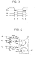
- FIG. 2 One example of the internal timing generator circuit 17 is illustrated in Fig. 2. As shown in this figure, the signals appearing on the respective address input terminals A o to An are respectively directly fed to one input terminals of corresponding Exclusive OR gates EX o to EX n , and also the signals on the respective address input terminals A o to An are respectively passed through delay circuits Do to D n and then fed to the other input terminals of the corresponding Exclusive OR gates EX o to EX n . Outputs OS o to OS n of the respective Exclusive OR gates are input to an OR gate RG, and thus an internal clock signal CE is output from the OR gate RG.
- the operation of the internal timing generator circuit 1.7 will be explained with reference to Fig. 3.
- the Exclusive OR gate EX o maintains a high level at its output for a period To until time point T 1 , because a delayed address signal DA o for the address A o does not follow the above logic change for a period corresponding to a delay time T d of the delay circuit Do.
- This high level output OS o is output as an internal clock signal CE via the OR gate RG.
- the delayed address DA o takes the same logic level as the address A o , so that the output OS o of the Exclusive OR gate EX o becomes a low level. Then, after the level of the address A o has returned to a anti high level at time point T 2 , again /coincidence between the address A o and the delayed address DA o occurs for the delay time T d of the delay circuit Do until time T 3 , so that the output OS o of the Exclusive OR gate EX o becomes high level and thus it is output as an internal clock signal CE at a high level.
- the pulse width of the above-described internal clock signal CE can be arbitrarily preset depending upon the delay characteristics of the delay circuits Do to D n .
- the delay circuits Do to D n can be designed without any restriction, for instance, by making use of inverter circuits on the like.
- EX n are led to respective input terminals of an (n+1) input flip-flop circuit FF having a reset terminal R.
- a reset signal which is generated when it is detected that in the memory circuit read-out corresponding to the changed address has been achieved.
- an internal synchronous type memory circuit is composed of an address inverter/buffer circuit 21, a row decoder circuit 22, a column decoder circuit 23, a memory cell array 24, a column selection circuit 25 an input/output circuit 26, an internal clock generator circuit 27 and an inverter 28.
- An internal clock signal CE generated by the internal clock generator circuit 27 and an inverted clock signal CE are fed to the above-referred respective circuits.
- the internal clock generator circuit 27 is constructed in such manner that as shown in Fig. 2, the address inputs A o , A 1 , Vietnamese , An are respectively fed to one inputs of the respective ones of the Exclusive OR circuits EX o , EX 1 , «
- the internal clock signal CE is used as a reset signal, while the inverted internal clock signal CE is used as an enable signal. Therefore, in the followings, the internal clock signals CE and CE are respectively referred to as “reset signal” and "enable signal”.
- FIG. 8 A timing diagram in this particular instance is illustrated in Fig. 8. Since the reset signal CE is turned to a high level each time the address input makes its logic change as described above. In case that a noise N is generated before a predetermined period T d elapses from time point T 81 when the address input A o made its logic change.
- the reset signal CE generated at time point T 81 further sustain the high level condition, and it turns to a low level when the predetermined period T d has elapsed after disappearance of the noise N.
- the memory circuit is held in a reset condition. Accordingly, by appropriately presetting this reset period T d , it is possible to prevent the memory circuit from being affected by the noise.
- an output would change dependent on whether an input signal exceeds a certain value, and this certain value is called “threshold value”.
- the rate of the change in the output to the change in the input in the neighborhood of the threshold value is generally not infinity, but there exists a transient region having a certain width.
- the output of the logic circuit is not at the logic level i. e. logic "1" or logic "0".
- the aforementioned transient region shall be called “insensitive region” with respect to an output throughout this specification. If an output of a logic circuit is not at logic level, then the logic circuit cannot achieve its inherent logic functions.
- FIG. 9 An inverter 21-i for one bit in the address inverter/buffer circuit 21 in Fig. 6 is shown in Fig. 9 as one example of a logic circuit.
- This inverter 21-i generates an inverted output A i in response to an input Ai.
- Input/output characteristics of this inverter 21-i are shown in Fig. 10, in which when the input Ai is outside of an insensitive region V 1 ⁇ V 2 , an output Ai is either at a first logic level having its minimum value at a level O 1 corresponding to logic "1" or at a second logic level having its maximum value at a level O 2 corresponding to logic "0".
- the output Ai is between the minimum value O 1 of the first logic level and the maximum value 0 2 of the second logic level, that is, the output Ai is not at the logic level. Accordingly, in case that the input Ai makes its logic change in a relatively slow manner and stays long in the insensitive region, the output Ai would remain in the non-logic level O 1 ⁇ 0 2 for that long period.
- a circuit shown in Fig. 11 comprises an address inverter 21-i and an internal clock generator circuit including a delay circuit and an Exclusive OR gate EXi which responds to the same address input Ai as that applied to the address inverter 21-i.
- an input Ai is in an insensitive region V 1 ⁇ V 2 with respect to an inverter output Ai, the output Ai cannot logically take a reliable value and cannot be utilized in a following stage of circuit (not shown). According to the present invention, such falling in insensitive region of Ai can be detected by the internal clock signal generator.
- An output OS i of the internal clock signal generator is supplied to an N-channel insulated-gate field-effect transistor Q 11-1 and a P-channel transistor Q 11-3 .
- the transistor Q 11-1 acts as a load element of the inverter 21-i and the transistor Q11-3 coupled between a source of an N-channel insulated-gate field-effect transistor Q 11-2 as a drive transistor and a ground potential is used to reset the inverter 21-i so that the state of the input Ai is inhibited to effect the output Ai.
- a logic circuit can be formed of NAND circuits or NOR circuits, and especially logic circuits constructed in an integrated circuit from are in most cases constructed of the aforementioned two basic circuits.
- an inverter circuit is equally applicable to these two basic circuits, i. e. , a NAND circuit and a NOR circuit.
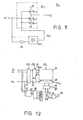
- the memory circuit comprises an address inverter buffer circuit 31, a row decoder circuit 32, a column decoder circuit 33, a memory cell array 34, a column selection circuit 35, an input/ output circuit 36, an internal timing generator circuit 37, a drive timing generator circuit 38 and an internal write signal generator circuit 39.
- the internal timing generator circuit 37 generates an internal clock signal CE when logic change occurs in at least one of the address inputs A o to An or when at least one of the address inputs is not at the rated logic levels.
- the drive timing generator circuit 38 responds to the internal clock signal CE for generating a plurality of timing signals CE1 to CE5 which are adapted for the control of the operations of the respective functional circuits as "enable signals".
- a timing signal CE2 is used for synchronizing the external write signal WE, and it is input to the internal write signal generator circuit 39.
- the internal write signal generator circuit 39 generates an internal write signal W which actually achieves write instruction within the memory circuit.
- the internal timing generator circuit 37 is equivalent to the circuit shown in Fig. 2 or Fig. 4.
- a row address input Ai changes at time point T71
- an internal clock signal CE is turned to a high level and it is turned to a low level at time point T 72 after a predetermined period T d .
- a control timing signal CE2 for the row and address decoder circuits 32 and 34 is held at a low level for the period T d from time point T 71 to time point T 72 to bring the address decoder circuits 32 and 33 to a reset condition, and it rises to a high level at time point T 72 to turn the address decoder circuits 32 and 33 to an enable condition.
- word lines WL k and WL1 l are both at a low level when the address decoder circuits 32 and 33 are in the reset condition, and at time point T 72 a selected word line WLt takes a high level.
- the external write WE that was applied at time point T 71 can be converted into an internal write signal W and introduced into the memory circuit for the first time when the control signal CE2 takes a high level at time point T 72 . Consequently, at time point T 72 it becomes possible to write in a selected memory cell.
- the external write signal WE takes a high level at time point T 73' the internal write signal W is turned to a low level, and then the write enable condition is terminated.
- an X-address inverter/buffer circuit includes P-channel IGFETs Q 1 , Q 2 , Q 4' Q 5 , Q 8 and Q 9 and N-channel IGFETs Q 3 , Q 6 , Q 7 , Q 10 and Q 11 constituting three stages of inverters.
- a X-decoder includes P-channel IGFETs Q 14 to Q 17 and N-channel IGFETs Q 51 to Q 57 .
- a control signal CE2 is applied to the gates of the P-channel IGFETs Q 14 and Q 15 , and when this control signal CE2 is at a low level, these transistors are conducted for resetting a NOR circuit including IGFETs Q 51 ⁇ Q 54 , as dynamic type load elements.
- P-channel IGFETs Q 15 - Q 17 and N-channel IGFETs Q 54 - Q 57 constitute a flip-flop type latch circuit which is reset in response to a low level of a control timing signal CE2' and enabled in response to its high level.
- the X-decoder circuit shifts to its enable state through its reset state caused by the signals CE2,CE2'.
- the signal CE2' may be replace by the signal CE2.
- the circuits are constructed in such manner that the respective singlessignals CE1 and CE2 are complementarily utilized on the side of the circuit elements instead of providing complementary signals CE1 and CE2.
- Each memory cell is composed of P-channel IGFETs Q P1 and Q P2 and N-channel IGFETs Q N1 and Q N2 , and in each memory cell a pair of cross coupled points are connected to a pair of digit lines D 1 and D 1 via N-channel IGFETs Q T1 and Q T2 , respectively, which serve as transfer gates with their gates connected in common to associated one word line WL k .
- These digit lines D 1 and D 1 are held in a reset condition, that is, precharged by P-channel IGFETs Q L1 , Q L2 and Q13 during the period when a control signal CE at a low level.
- a Y-decoder 42 has a similar circuit structure as the X-decoder, and it is rest when the control signals CE2 and CE2' at a low level and is held in an enable condition when the control signals CE2 and CE2' are at a high level. In an enable condition, the Y-decoder 42 controls Y-select IGFETs Q 60 , Q Y1 and Q Y2 .
- An output latch circuit 43 receives the output of the sense amplifier via N-channel IGFETs Q 27 and Q 28 , and in response to a high level of a control signal CE4 it holds the output and drives a push-pull type output circuit consisting of P-channel IGFETs Q 25 and Q 26 to feed the output to an input/output terminal I/O.
- P-channel IGFETs Q 18 to Q 20 have a reset function for the write circuit, and they precharge write bus lines DB and DB in response to a control signal CE5 at a low level.
- NAND gates NA 1 and NA 2 and P-channel IGFETs Q 21 to Q 24 form a write drive circuit, which operates in such manner that when the control signal CE5 is at a high level, in response to a high level of an internal write signal W produced by AND gate AG receiving the signal CE2 and the write signal WE the data at the input/output terminal I/O may be applied in a complementary form to the write bus lines DB and DB through two push-pull type inverters,' respectively.
- Fig. 15 is illustrated one example of timing relationship between the internal clock signal OS i generated in response to change of the address and the respective control signals CE1 to CE5 which are generated on the basis of the signal OSi caused by address input change (Ai) through a well-known process and which are adapted to the respective functional circuits. Then the data output (at the terminal I/O) would be data accessed after termination of resetting of the respective functional blocks.
- the respective functional circuits can be controlled substantially by means of a single control signal.
- stationary currents flowing through the respective functional blocks can be greatly reduced.
- An OR gate OR 1 is enactly the same as the OR gate R in Fig. 2 and address change detection outputs OS o to OS n for the respective address inputs A o to An are input to this OR gate OR 1 .
- the control signal CE1 is derived from the output of the OR gate OR 1 .
- the other control signals CE2 to CE6 are derived from the control signal CE1 through a circuit consisting of a NOR gate NR 1 , OR gates OR2 to OR7 , inverters 1N 1 and 1N 2 and delay circuits DL 1 to DL 6 as shown in Fig. 16.
- the control signal CE6 is generated only upon write operation.
- the delay circuit (D o ⁇ D n ) and the Exclusive OR gate (EX 1 ⁇ EX n ) are employed in the internal clock (timing) signal generator circuit.
- the internal clock signal generator circuit according to the present invention is not limited to such a structure.
- FIG. 17 one bit unit of structure for the circuit for detecting a change in the input Ai in logic level or non-logic level of the input Ai is illustrated.
- an inverter circuit INT 1 having a logic threshold value V T1 and an inverter circuit INT 2 having a logic threshold value V T2 are coupled between the input A i and the respective input terminals of the Exclusive OR circuit EXi.
- the threshold value V T1 is at a voltage near the high level of the input signal Ai and a slightly smaller voltage than it.
- the threshold voltage V TZ is at the low level of the input signal A i and slightly larger than it.
- the transient in the input signal Ai i. e. the non-logic level thereof can be detected based on a difference of the threshold values V T1 and V T2 .
- the level of the input signal Ai starts to fall from the high-level to the low level.
- the level of the signal A i becomes lower than the threshold value V T1 and an output VO 1 of the inverter INT 1 starts to rise while an output VO 2 of the inverter INT 2 remains at the low level.
- the level of the signal becomes lower than the threshold value V T2 and hence the output VO Z starts to rise.
- the rising level of the output VO 1 exceeds a threshold value V T0 of the Exclusive OR gate EXi and hence the output OS i starts to rise in level.
- the output VO 2 reaches the high level and hence the output OS i starts to fall.
- the detection signal (OSi) is generated based on the change in the signal Ai.
- inverter circuits as cascaded in n stages as a whole are represented by the following equations (2) and (3): where mi represents a gain of the i-th inverter, and V k represents a threshold value of the k-th inverter.
- the insensitive region can be arbtrarily preset according to equations (2) and (3) above by appropriately relating the characteristics of the individual inverters. Therefore, the inverter circuit such as INT 1 , INT 2 having optional threshold voltage can be realized base on the equation(3).
Abstract
Description
- The present invention relates to an integrated circuit, and more particularly to a memory device fabricated as a semiconductor integrated circuit (IC memory).
- IC memories are generally classified into the so-called synchronous type memories in which various functional circuits therein such as decoders, sense amplifiers, input/output circuits, etc. are controlled by clock signals, and the so-called asynchronous type memories which does not receive a clock signal and can operate without undergoing any restriction in time, replying only upon input signals such as address information and the like. Although the synchronous type memories are more excellent than the asynchrous type memories with respect to a speed-power product which is normally used as a figure of merit for representing a performance, they necessitate external terminals for receiving clock signals which imposes large restriction upon practical design of ICs, as well as increase in the number of external terminals caused by enhancement of a memory capacity. Moreover, in the synchronous memory, there exists restriction in timing between input data and clock signals since input data such as address information, write information, etc. are introduced into the interior of the IC memory in synchronism with the clock signals in any way. This means that even if address information is fed to the IC memory asynchronously with a clock signal, for instance, the address information will be not accepted at all by the memory and thus will become ineffective. Accordingly, the synchronous type memories have a disadvantage that they are inconvenient for use.
- On the other hand, in an asynchronous type memory, input data such as address information can be accepted at any arbitrary time and immediately introduced into the interior of the memory at the time point of acceptance to achieve the operation corresponding to the input data, and therefore, it is easy for use. However, in the asynchronous type memory every functional circuit is always in an operating condition, and hence it has a disadvantage that always large power is dissipated therein.
- Above arguments between the synchronous type memory and the asynchronous type memory can be similarly expanded to general integrated circuits which are classified into a synchronous type logic integrated circuit such as a dynamic type logic integrated circuit and a asynchronous type logic integrated circuit such as a static type logic integrated circuit. In this expansion of arguments, the synchrous type logic integrated circuit has substantially the same advantage and the same disadvantage as those of the synchronous type memory while the asynchrous type logic integrated circuit has substantially the same advantage and the same disadvantage as those of the asynchronous type memory. Furthermore, in the asynchronous type logic integrated circuit in which a plurality stage of logic circuit are coupled in cascade, a non-logic level which cannot be classified into any one of rated two logic levels i.e. logic "1" and logic "0" levels inevitably appears at an output of a first stage of logic circuit during a transient time when an input changes in logic level. Such a non-logic level is directly transferred to the succeeding stages of logic circuits and hence the final stage of the logic circuit frequently produces an erroneous output.
- Therefore, it is one object of the present invention to provide a memory device which incorporates only the merit of the asynchronous type memories and only the merit of the synchronous type memories in combination.
- Another object of the present invention is to provide a memory device which has a reduced number of terminals and less power dissipation.
- Still another object of the present invention is to provide an integrated circuit operable with high- reliability.
- An integrated circuit according to the present invention comprises a logic circuit receiving logic input signal at its input, means for detecting a change in the input signal from one logic level to the other logic level or non-logic level of the input signal.not falling into either of binary logic levels to produce a control signal, and means responsive to the control signal for resetting the logic state of the logic circuit.
- According to one aspect of the present invention, there is provided a memory device in which a clock signal (an internal clock signal) is generated inside the memory device without receiving a clock signal from the outside, and the internal clock signal is generated only when logic change has occurred in at least one address input.
- According to another aspect of the present invention, there is provided a memory device comprising means for detecting logic change in address inputs information, and means for generating an internal clock signal only when logic change has occurred in the address input information.
- According to still another aspect of the present invention there is provided an above-featured memory device in which the detecting means is compossed of delay circuits for delaying the respective address inputs and Exclusive OR circuits each having one of the address inputs applied to its first input and the output of the corresponding delay circuit applied to its second input, and the internal clock signal generating means is composed of a multi-input flip-flop circuit having a reset terminal which has the respective outputs of the Exclusive OR circuits applied to its inputs.
- The integrated circuit according to the present invention can reduce the number of external terminals because it does not necessitate to receive clock signals externally.
- In the integrated circuit such as memory device according to the present invention, input data are not introduced in synchronism with a clock signal as is the case with the synchronous type memory in the prior art, but in response to change in the input data itself, that is, in response to new demand for access, a control signal for executing the demand for access is generated within the circuit. Consequently, input data can be accepted at any arbitrary time, and also less power dissipation can be realized.
- Now the invention will be described in greater detail with reference to the accompanying drawings.
-
- Fig. 1 is a block diagram showing a memory device according to a first preferred embodiment of the present invention;
- Fig. 2 is a block diagram showing one example of an internal clock generator circuit that is available in the preferred embodiment shown in Fig. 1;
- Fig. 3 is a waveform diagram showing the operations of the circuit in Fig. 2,
- Fig. 4 is a block diagram showing another example of an internal clock generator circuit that is available in the preferred embodiment shown in Fig. 1;
- Fig. 5 is a waveform diagram showing the operations of the circuit in Fig. 4;
- Fig. 6 is a block diagram showing a memory device according to a second preferred embodiment of the present invention;
- Fig. 7 is a waveform diagram showing one example of operation of the memory device in Fig. 6;
- Fig. 8 is a waveform diagram showing another example of the operation of the memory device in Fig. 6;
- Fig. 9 is a block diagram showing an inverter to be used in an address inverter buffer circuit in the memory device shown in Fig. 6;
- Fig. 10 is a diagram showing an input/output characteristic of the inverter shown in Fig. 9;
- Fig. 11 is a block diagram showing an inverter and an internal clock generator circuit for one bit of address input according to the present invention;
- Fig. 12 is a block diagram showing a memory device according to a third preferred embodiment of the present invention;
- Fig. 13 is a waveform diagram showing operations of the memory device in Fig. 2;
- Fig. 14 is a circuit diagram showing a detailed circuit arrangement in a memory device according to the present invention:
- Fig. 15 is a waveform diagram showing various control signals used in the circuit shown in Fig. 14.
- Fig. 16 is a block diagram showing a control timing generator circuit;
- Fig. 17 is a block diagram showing another example of the internal clock signal generator circuit; and
- Fig. 18 is a wave form diagram showing operation of the circuit of Fig. 17;
- Now a first preferred embodiment of the present invention will be described with reference to Figs. 1 to 3.
- A basic structure of the memory device according to the present invention is illustrated in Fig. 1. In this figure, a plural bits of address inputs Ao to An are applied to an address inverter/
buffer 11, which generates true and complementary address signals for the respective address inputs Ao to An, a part of the address signals are fed to arow decoder 12, and the remainder of the address signals are fed to acolumn decoder 13. In response to the address signals, therow decoder 12 brings one of word lines in amemory cell matrix 14 to a selection level, while thecolumn decoder 13 responds to the address signals to control aselection circuit 15 so as to selectively supply data on one digit line or one pair of digit lines in thememory cell matrix 14 to an input/output circuit 16. The data selected by theselection circuit 15 are output via the input/output circuit 16 to an input/output terminal I/O. The input/output circuit 16 is brought into a read condition in response to a high level at a read/write control terminal WE, and is brought into a write condition in response to a low level at the read/write control terminal WE. The above-mentioned component parts are constructed in the well-known manner. According to the present invention, there is provided an internaltiming generator circuit 17 which generates an internal clock signal CE when the address inputs Ao to An are applied thereto and then change has occurred in the address information represented by the address inputs Ao to An. An enable control signal CE is fed to respective functional circuits such as the addressinverter buffer circuit 11 and the like to control their operations. The respective functional circuits are enabled by a high level of the enable control signal CE. - One example of the internal
timing generator circuit 17 is illustrated in Fig. 2. As shown in this figure, the signals appearing on the respective address input terminals Ao to An are respectively directly fed to one input terminals of corresponding Exclusive OR gates EXo to EXn, and also the signals on the respective address input terminals Ao to An are respectively passed through delay circuits Do to Dn and then fed to the other input terminals of the corresponding Exclusive OR gates EXo to EXn. Outputs OSo to OSn of the respective Exclusive OR gates are input to an OR gate RG, and thus an internal clock signal CE is output from the OR gate RG. - The operation of the internal timing generator circuit 1.7 will be explained with reference to Fig. 3. Here, by way of example, let us assume that among the address inputs Ao to An, one address Ao has made logic change. When the address Ao makes logic change at time point To, the Exclusive OR gate EXo maintains a high level at its output for a period To until time point T1, because a delayed address signal DAo for the address Ao does not follow the above logic change for a period corresponding to a delay time Td of the delay circuit Do. This high level output OSo is output as an internal clock signal CE via the OR gate RG. After the time point T1, the delayed address DAo takes the same logic level as the address Ao, so that the output OSo of the Exclusive OR gate EXo becomes a low level. Then, after the level of the address Ao has returned to a anti high level at time point T2, again /coincidence between the address Ao and the delayed address DAo occurs for the delay time Td of the delay circuit Do until time T3, so that the output OSo of the Exclusive OR gate EXo becomes high level and thus it is output as an internal clock signal CE at a high level.
- As described above, according to the present invention, advantages are obtained that since a clock input terminal need not be provided, the number of terminals can be reduced, and that since internal clock signals are generated only upon access, that is, only when an address is changed, a power dissipation can be greatly reduced.
- It is to be noted that the pulse width of the above-described internal clock signal CE can be arbitrarily preset depending upon the delay characteristics of the delay circuits Do to Dn. In addition, the delay circuits Do to Dn can be designed without any restriction, for instance, by making use of inverter circuits on the like.
- Next, another example of the internal
clock generator circuit 17 to be used according to the present invention will be described with reference to Figs. 4 and 5. - In Fig. 4, address inputs Ao, A1, ..... , An are supplied to input terminals of delay circuits Do, D1, ...... Dn, respectively, and respective first inputs of Exclusive OR circuits EXo, EX1, ..... , EXn. Output terminals DAo, DA1, ..... , DAn of the delay circuits Do, D1, .... , Dn are respectively connected to respective second inputs of the Exclusive OR circuits EXo, EX1, ...... , Exn. Outputs OSo, OS1, ..... , OSn of the Exclusive OR circuits EXo, EX1, ..... , EXn are led to respective input terminals of an (n+1) input flip-flop circuit FF having a reset terminal R. To the reset terminal R of the flip-flop FF is fed a reset signal which is generated when it is detected that in the memory circuit read-out corresponding to the changed address has been achieved.
- Now, one example of the operation of the internal clock generator circuit shown in Fig. 4 will be described with reference to Fig.5. At time point To, if the address input Ao changes from logic "1" to logic "0", then the output OSo of the Exclusive OR circuit EXo changes from "0" to "1", so that the output CE of the flip-flop circuit FF changes from "0" to "1". When the output DAo, of the delay circuit Do changes from "1" to "0" at time point Tl, the output OSo of the exclusive OR circuit EXo changes from "1" to "0", but the output CE of the flip-flop FF still remain at "1" because the output CE has been already latched in the flip-flop FF. At time point T2, if a reset signal R changes from "0" to "1" in response to completion of the read operation based on the changed address information, then the flip-flop FF is turned to its reset condition, and hence the output CE changes from "1" to "0". In the case where the address input Ao changes from "0" to "1" at time point T4 also, a similar operation for next access to the above-described operation will be effected, and thus the output CE will change again from "0" to "1".
- While description has been made above on the operation where only the address input Ao changes in logic level, it is obvious that a similar operation will be effected also where more than one address inputs have changed in logic level.
- In the followings, a second preferred embodiment of the present invention will be described with reference to Figs. 6 to 11.
- In Fig. 6 an internal synchronous type memory circuit is composed of an address inverter/
buffer circuit 21, arow decoder circuit 22, acolumn decoder circuit 23, amemory cell array 24, acolumn selection circuit 25 an input/output circuit 26, an internalclock generator circuit 27 and aninverter 28. An internal clock signal CE generated by the internalclock generator circuit 27 and an inverted clock signal CE are fed to the above-referred respective circuits. The internalclock generator circuit 27 is constructed in such manner that as shown in Fig. 2, the address inputs Ao, A1, ..... , An are respectively fed to one inputs of the respective ones of the Exclusive OR circuits EXo, EX1, ...... EXn and to the respective inputs of the delay circuits Do, D1, ...... Dn. The outputs DAo, DA1, ..... , DAn of the delay circuits Do, D1, ..... , Dn are fed to the other inputs of the respective ones of the Exclusive OR circuits EXo, EX1, ..... , EXn, and the respective outputs OSo, OS1, ..... , OSn of the respective ones of the exclusive OR circuits EXo, EX1, ..... , EXn are supplied to the OR circuit RG. The internal clock signal CE is output from the OR circuit RG. In the second preferred embodiment, the internal clock signal CE is used as a reset signal, while the inverted internal clock signal CE is used as an enable signal. Therefore, in the followings, the internal clock signals CE and CE are respectively referred to as "reset signal" and "enable signal". - Now operations of the circuit shown in Fig. 6 will be described, by way of example, in connection to the case where the address input Ao has made its logic change. As shown in Fig. 7, in response to the logic change of the address input Ao, a reset signal CE is generated. At the same time, the enable signal CE takes a low level and thus the memory circuit is brought into a reset condition. After the resent condition has continued for a predetermined period Td determined by the delay circuit in the
circuit 27, the reset signal CE takes a low level. At the same time, the enable signal CE changes to a high level, and hence the memory circuit is brought into an enable condition. Here let us assume that a noise N arises in the address input Ao as shown by a broken line in Fig. 7. A timing diagram in this particular instance is illustrated in Fig. 8. Since the reset signal CE is turned to a high level each time the address input makes its logic change as described above. In case that a noise N is generated before a predetermined period Td elapses from time point T81 when the address input Ao made its logic change. - Then the reset signal CE generated at time point T81 further sustain the high level condition, and it turns to a low level when the predetermined period Td has elapsed after disappearance of the noise N. In other words, for a predetermined period Td after the disappearance of the noise N, the memory circuit is held in a reset condition. Accordingly, by appropriately presetting this reset period Td, it is possible to prevent the memory circuit from being affected by the noise.
- While description has been made above in connection to the case where a noise N as shown in Figs. 7 and 8 has occurred in the address input Ao, it is obvious that a noise having whatever delay and whatever width may arise in any one or plurality of address inputs, the memory circuit according to the present invention can operate correctly.
- Description has been made to the cases where the present invention is applied to the memory devices. However, the application of the subject matter of the present invention, especially the internal clock generator, is not limited to memory devices but can be expanded to a logic integrated circuit implementing digital operations. In the following . the logic circuit according to the present invention will be described with reference to Figs. 9 to 11, in which description will be made on an address inverter employed in part of the address inverter/buffer circuit in the memory device as one example, which will also clarify another basic effect and advantage of the present invention in addition to the above-described effect and advantage.
- In general, in a logic circuit an output would change dependent on whether an input signal exceeds a certain value, and this certain value is called "threshold value". However, the rate of the change in the output to the change in the input in the neighborhood of the threshold value is generally not infinity, but there exists a transient region having a certain width. In other words, when the input signal is in this transient region, the output of the logic circuit is not at the logic level i. e. logic "1" or logic "0". In this mean, the aforementioned transient region shall be called "insensitive region" with respect to an output throughout this specification. If an output of a logic circuit is not at logic level, then the logic circuit cannot achieve its inherent logic functions. Moreover if such condition should continue for a predetermined period, sometimes inconvenience would occur such that an abnormal current flows through the circuit or the logic condition is reversed to a wrong side. Therefore, in such a case, it was necessary to impose restriction upon the input of the logic circuit that it must not stay in the insensitive region longer than a predetermined period. This will be explained in more detail in the followings, by way of example, in connection to an address inverter.
- An inverter 21-i for one bit in the address inverter/
buffer circuit 21 in Fig. 6 is shown in Fig. 9 as one example of a logic circuit. This inverter 21-i generates an inverted output Ai in response to an input Ai. Input/output characteristics of this inverter 21-i are shown in Fig. 10, in which when the input Ai is outside of an insensitive region V1 ~ V2, an output Ai is either at a first logic level having its minimum value at a level O1 corresponding to logic "1" or at a second logic level having its maximum value at a level O2 corresponding to logic "0". However, when the input Ai is within the insensitive region V1 ~ V2, the output Ai is between the minimum value O1 of the first logic level and the maximum value 02 of the second logic level, that is, the output Ai is not at the logic level. Accordingly, in case that the input Ai makes its logic change in a relatively slow manner and stays long in the insensitive region, the output Ai would remain in the non-logic level O1 ~ 02 for that long period. - Now a circuit for obviating the above-described disadvantage of logic circuits by making use of an internal clock generator circuit according to the present invention, will be described, by way of example, in connection to an inverter 21-i with reference to Fig. 11.
- A circuit shown in Fig. 11 comprises an address inverter 21-i and an internal clock generator circuit including a delay circuit and an Exclusive OR gate EXi which responds to the same address input Ai as that applied to the address inverter 21-i. When an input Ai is in an insensitive region V1 ~ V2 with respect to an inverter output Ai, the output Ai cannot logically take a reliable value and cannot be utilized in a following stage of circuit (not shown). According to the present invention, such falling in insensitive region of Ai can be detected by the internal clock signal generator. An output OSi of the internal clock signal generator is supplied to an N-channel insulated-gate field-effect transistor Q11-1 and a P-channel transistor Q11-3. The transistor Q11-1 acts as a load element of the inverter 21-i and the transistor Q11-3 coupled between a source of an N-channel insulated-gate field-effect transistor Q11-2 as a drive transistor and a ground potential is used to reset the inverter 21-i so that the state of the input Ai is inhibited to effect the output Ai.
- As described above, in such a logic circuit, when the input is not at the logic levels, a detection output for notifying the fact is delivered, and hence by making use of the detection output it is possible to prevent occurrence of inconvenience such that any device or circuit to which the logic signal is to be applied is forcibly returned to its reset condition. Accordingly, there is no need to impose restriction upon a logic circuit such that its input must not stay for more than a predetermined period.
- While a method for ovecoming the disadvantage with respect to an insensitive region of a logic circuit has been proposed and explained above, by way of example, in connection to an inverter circuit, it is obvious that the proposed method is also applicable to logic circuits having different functions.
- In general, a logic circuit can be formed of NAND circuits or NOR circuits, and especially logic circuits constructed in an integrated circuit from are in most cases constructed of the aforementioned two basic circuits. Obviously, the above discussion with respect to an inverter circuit is equally applicable to these two basic circuits, i. e. , a NAND circuit and a NOR circuit. Thus description has been made above in connection to the method for presetting an insensitive region at a desired value.
- Now a third preferred embodiment of the present invention will be described with reference to Figs. 12 and 13.
- Generally in a write cycle of an asynchronous type memory circuit not employing an external clock signal, a time from logic change of an address input to input of an externally applied write signal (external write signal) is prescribed, and normally this is called "address set-up time tAS". This implies that in order to prevent wrong writing at an address selected in a cycle preceding to the write cycle in question, there is provided a predetermined restriction in time such as, for example, a delay time between an address input and an external write signal so that an internal write signal corresponding to the external write signal WE may arise after the word line or bit line corresponding to the previously selected address has become unselected. However, the above-mentioned delay time would largely vary due to fluctuation in manufacture, variation of a power supply voltage and the like, and hence it is necessary to design the circuit with a sufficient margin for the variations. Therefore, this type of memory circuit in the prior art had the disadvantages that not only the estimation of the margin was in itself difficult, but also the width of the internal write signal was shortened by incorporating the margin, thus reliable writing became difficult and high speed operations became difficult. According to the illustrated embodiment, there is provided a memory circuit in which the aforementioned disadvantages relating to the address set-up time tAS are eliminated and there is no need to incorporate the margin for the fluctuations in manufacture and the like.
- In Fig. 12, the memory circuit comprises an address
inverter buffer circuit 31, a row decoder circuit 32, acolumn decoder circuit 33, a memory cell array 34, acolumn selection circuit 35, an input/output circuit 36, an internaltiming generator circuit 37, a drivetiming generator circuit 38 and an internal writesignal generator circuit 39. The internaltiming generator circuit 37 generates an internal clock signal CE when logic change occurs in at least one of the address inputs Ao to An or when at least one of the address inputs is not at the rated logic levels. The drivetiming generator circuit 38 responds to the internal clock signal CE for generating a plurality of timing signals CE1 to CE5 which are adapted for the control of the operations of the respective functional circuits as "enable signals". A timing signal CE2 is used for synchronizing the external write signal WE, and it is input to the internal writesignal generator circuit 39. The internal writesignal generator circuit 39 generates an internal write signal W which actually achieves write instruction within the memory circuit. The internaltiming generator circuit 37 is equivalent to the circuit shown in Fig. 2 or Fig. 4. - Now the operation of the memory circuit shown in Fig. 12 will be described with reference to a timing chart illustrated in Fig. 13. When a row address input Ai changes at time point T71, an internal clock signal CE is turned to a high level and it is turned to a low level at time point T72 after a predetermined period Td. A control timing signal CE2 for the row and address decoder circuits 32 and 34 is held at a low level for the period Td from time point T71 to time point T72 to bring the
address decoder circuits 32 and 33 to a reset condition, and it rises to a high level at time point T72 to turn theaddress decoder circuits 32 and 33 to an enable condition. In response to such change in condition, word lines WLk and WL1ℓ are both at a low level when theaddress decoder circuits 32 and 33 are in the reset condition, and at time point T72 a selected word line WLt takes a high level. On the other hand, the external write WE that was applied at time point T71 can be converted into an internal write signal W and introduced into the memory circuit for the first time when the control signal CE2 takes a high level at time point T72. Consequently, at time point T72 it becomes possible to write in a selected memory cell. When the external write signal WE takes a high level at time point T73' the internal write signal W is turned to a low level, and then the write enable condition is terminated. - As will be apparent from the above description, since the internal write signal W is generated in synchronism with the control signal CE2 which controls the
address decoder circuits 32 and 33, it would never occur that data are written into the preceeding address which was selected in the previous cycle. In other words, the requirement for the address setup time tAS could be logically fulfilled, and so there is no need to provide a margin in design for the fluctuations in manufacture, variations of a power supply voltage and the like. - Now a detailed circuit arrangement for embodying the present invention will be described with reference to Figs. 14 to 16. In the practical example of the memory circuit shown in Fig. 15, a C-MOS structure employing P-channel insulated-gate field-effect transistors (IGFETs) and N-channel IGFETs is illustrated. In this circuit, an X-address inverter/buffer circuit includes P-channel IGFETs Q1, Q2, Q4' Q5, Q8 and Q9 and N-channel IGFETs Q3, Q6, Q7, Q10 and Q11 constituting three stages of inverters. When a control signal CE1 is at a low level, this address inverter buffer circuit is in a reset condition, and it is brought into an enable condition when the control signal CE1 is turned to a high level. A X-decoder includes P-channel IGFETs Q14 to Q17 and N-channel IGFETs Q51 to Q57. In this X-decoder, a control signal CE2 is applied to the gates of the P-channel IGFETs Q14 and Q15, and when this control signal CE2 is at a low level, these transistors are conducted for resetting a NOR circuit including IGFETs Q51 ~ Q54, as dynamic type load elements. Also in the X-decoder, P-channel IGFETs Q15 - Q17 and N-channel IGFETs Q54 - Q57 constitute a flip-flop type latch circuit which is reset in response to a low level of a control timing signal CE2' and enabled in response to its high level. Thus, the X-decoder circuit shifts to its enable state through its reset state caused by the signals CE2,CE2'. In this connection, the signal CE2' may be replace by the signal CE2.
- As described above, in the illustrated embodiment, the circuits are constructed in such manner that the respective singlessignals CE1 and CE2 are complementarily utilized on the side of the circuit elements instead of providing complementary signals CE1 and CE2.
- Each memory cell is composed of P-channel IGFETs QP1 and QP2 and N-channel IGFETs QN1 and QN2, and in each memory cell a pair of cross coupled points are connected to a pair of digit lines D1 and D1 via N-channel IGFETs QT1 and QT2, respectively, which serve as transfer gates with their gates connected in common to associated one word line WLk. These digit lines D1 and D1 are held in a reset condition, that is, precharged by P-channel IGFETs QL1, QL2 and Q13 during the period when a control signal CE at a low level.
- P-channel IGFETs Q29 to Q31 and N-channel IGFETs Q58 to Q61 from a selection sense amplifier, which is held in a reset condition during the period when the control signal CE4' is at a low level, and which is held in an enable condition during the period when the control signal CE4' is at a high level.
- A Y-
decoder 42 has a similar circuit structure as the X-decoder, and it is rest when the control signals CE2 and CE2' at a low level and is held in an enable condition when the control signals CE2 and CE2' are at a high level. In an enable condition, the Y-decoder 42 controls Y-select IGFETs Q60, QY1 and QY2. - An
output latch circuit 43 receives the output of the sense amplifier via N-channel IGFETs Q27 and Q28, and in response to a high level of a control signal CE4 it holds the output and drives a push-pull type output circuit consisting of P-channel IGFETs Q25 and Q26 to feed the output to an input/output terminal I/O. - P-channel IGFETs Q18 to Q20 have a reset function for the write circuit, and they precharge write bus lines DB and DB in response to a control signal CE5 at a low level. NAND gates NA1 and NA2 and P-channel IGFETs Q21 to Q24 form a write drive circuit, which operates in such manner that when the control signal CE5 is at a high level, in response to a high level of an internal write signal W produced by AND gate AG receiving the signal CE2 and the write signal WE the data at the input/output terminal I/O may be applied in a complementary form to the write bus lines
DB and DB through two push-pull type inverters,' respectively. - In Fig. 15 is illustrated one example of timing relationship between the internal clock signal OSi generated in response to change of the address and the respective control signals CE1 to CE5 which are generated on the basis of the signal OSi caused by address input change (Ai) through a well-known process and which are adapted to the respective functional circuits. Then the data output (at the terminal I/O) would be data accessed after termination of resetting of the respective functional blocks.
- In the illustrated embodiment, since a C-MOS structure is employed, the respective functional circuits can be controlled substantially by means of a single control signal. In addition, stationary currents flowing through the respective functional blocks can be greatly reduced.
- Next, a circuit for generating the respective control signals CE1 to CE5 as appearing in Figs. 14 and 15 will be described with reference to Fig. 16. An OR gate OR1 is enactly the same as the OR gate R in Fig. 2 and address change detection outputs OSo to OSn for the respective address inputs Ao to An are input to this OR gate OR1. The control signal CE1 is derived from the output of the OR gate OR1. The other control signals CE2 to CE6 are derived from the control signal CE1 through a circuit consisting of a NOR gate NR1, OR gates OR2 to OR7, inverters 1N1 and 1N2 and delay circuits DL1 to DL6 as shown in Fig. 16. The control signal CE6 is generated only upon write operation.
- In the above description, the delay circuit (Do ~ Dn) and the Exclusive OR gate (EX1 ~ EXn) are employed in the internal clock (timing) signal generator circuit. However, the internal clock signal generator circuit according to the present invention is not limited to such a structure.
- In the following, another example of the internal clock signal circuit will be described with reference to Figs. 17 and 18.
- In Fig. 17, one bit unit of structure for the circuit for detecting a change in the input Ai in logic level or non-logic level of the input Ai is illustrated. In this scheme, an inverter circuit INT1 having a logic threshold value VT1 and an inverter circuit INT2 having a logic threshold value VT2 are coupled between the input Ai and the respective input terminals of the Exclusive OR circuit EXi. The threshold value VT1 is at a voltage near the high level of the input signal Ai and a slightly smaller voltage than it. The threshold voltage VTZ is at the low level of the input signal Ai and slightly larger than it. In this structure, the transient in the input signal Ai, i. e. the non-logic level thereof can be detected based on a difference of the threshold values VT1 and VT2.
- Operation of the circuit in Fig. 17 will be described with reference to Fig. 18.
- From time point to, the level of the input signal Ai starts to fall from the high-level to the low level. At time point tl, the level of the signal Ai becomes lower than the threshold value VT1 and an output VO1 of the inverter INT1 starts to rise while an output VO2 of the inverter INT2 remains at the low level. Then, at time point t2, the level of the signal becomes lower than the threshold value VT2 and hence the output VOZ starts to rise. The rising level of the output VO1 exceeds a threshold value VT0 of the Exclusive OR gate EXi and hence the output OSi starts to rise in level. Then at time point t4, the output VO2 reaches the high level and hence the output OSi starts to fall. Thus, the detection signal (OSi) is generated based on the change in the signal Ai.
- Now a method for presetting the threshold voltage at any desired value will be explained. At first, let us consider an inverter circuit. Input/output characteristics of an inverter circuit in the proximity of the insensitive region are represented by the following equation (1) :


Claims (8)
Applications Claiming Priority (8)
| Application Number | Priority Date | Filing Date | Title |
|---|---|---|---|
| JP46848/79 | 1979-04-17 | ||
| JP4684879A JPS55138128A (en) | 1979-04-17 | 1979-04-17 | Memory circuit |
| JP14417879A JPS5668030A (en) | 1979-11-07 | 1979-11-07 | Logic circuit |
| JP144178/79 | 1979-11-07 | ||
| JP14469479A JPS5668990A (en) | 1979-11-08 | 1979-11-08 | Memory circuit |
| JP144693/79 | 1979-11-08 | ||
| JP144694/79 | 1979-11-08 | ||
| JP14469379A JPS5668989A (en) | 1979-11-08 | 1979-11-08 | Memory circuit |
Publications (2)
| Publication Number | Publication Date |
|---|---|
| EP0017990A1 true EP0017990A1 (en) | 1980-10-29 |
| EP0017990B1 EP0017990B1 (en) | 1985-04-03 |
Family
ID=27461946
Family Applications (1)
| Application Number | Title | Priority Date | Filing Date |
|---|---|---|---|
| EP80102068A Expired EP0017990B1 (en) | 1979-04-17 | 1980-04-17 | Integrated memory circuit |
Country Status (3)
| Country | Link |
|---|---|
| US (1) | US4337525A (en) |
| EP (1) | EP0017990B1 (en) |
| DE (1) | DE3070410D1 (en) |
Cited By (13)
| Publication number | Priority date | Publication date | Assignee | Title |
|---|---|---|---|---|
| EP0043245A2 (en) * | 1980-06-30 | 1982-01-06 | Inmos Corporation | Asynchronously equilibrated and pre-charged static RAM |
| FR2496955A1 (en) * | 1980-12-22 | 1982-06-25 | Fairchild Camera Instr Co | ADDRESSING DOOR FOR MEMORY AND METHOD OF USING SAME |
| EP0083195A2 (en) * | 1981-12-28 | 1983-07-06 | Fujitsu Limited | Decoder circuit for a semiconductor device |
| EP0096421A2 (en) * | 1982-06-09 | 1983-12-21 | Kabushiki Kaisha Toshiba | Static memory device with signal transition detector |
| EP0115140A2 (en) * | 1982-12-27 | 1984-08-08 | Fujitsu Limited | Decoder circuit |
| EP0128499A2 (en) * | 1983-06-03 | 1984-12-19 | Hitachi, Ltd. | MOS memory |
| EP0158028A2 (en) * | 1984-02-27 | 1985-10-16 | Kabushiki Kaisha Toshiba | Random access memory device |
| EP0180895A2 (en) * | 1984-10-29 | 1986-05-14 | Nec Corporation | Memory circuit with improved power-down control |
| EP0181177A2 (en) * | 1984-11-05 | 1986-05-14 | Fujitsu Limited | A semiconductor memory device |
| EP0199458A2 (en) * | 1985-03-18 | 1986-10-29 | Nec Corporation | Memory circuit having an improved writing scheme |
| EP0273652A2 (en) * | 1986-12-19 | 1988-07-06 | Fujitsu Limited | Pseudo-static memory device having internal self-refresh circuit |
| EP0498895A1 (en) * | 1990-09-05 | 1992-08-19 | Fujitsu Limited | Semiconductor integrated circuit |
| EP0678869A1 (en) * | 1994-02-18 | 1995-10-25 | STMicroelectronics S.r.l. | Method and circuit for timing the loading of non-volatile memory output data. |
Families Citing this family (26)
| Publication number | Priority date | Publication date | Assignee | Title |
|---|---|---|---|---|
| JPS5952492A (en) * | 1982-09-17 | 1984-03-27 | Fujitsu Ltd | Static semiconductor storage device |
| JPS5957525A (en) * | 1982-09-28 | 1984-04-03 | Fujitsu Ltd | Cmis circuit device |
| JPS5958688A (en) * | 1982-09-29 | 1984-04-04 | Fujitsu Ltd | Decoder circuit |
| JPS5963094A (en) * | 1982-10-04 | 1984-04-10 | Fujitsu Ltd | Memory device |
| US4467455A (en) * | 1982-11-01 | 1984-08-21 | Motorola, Inc. | Buffer circuit |
| JPS59221891A (en) * | 1983-05-31 | 1984-12-13 | Toshiba Corp | Static semiconductor storage device |
| JPS60253091A (en) * | 1984-05-30 | 1985-12-13 | Fujitsu Ltd | Semiconductor storage device |
| US4661931A (en) * | 1985-08-05 | 1987-04-28 | Motorola, Inc. | Asynchronous row and column control |
| JPS6342090A (en) * | 1986-08-07 | 1988-02-23 | Fujitsu Ltd | Signal change detection circuit |
| FR2606199B1 (en) * | 1986-11-04 | 1988-12-09 | Eurotechnique Sa | INTEGRATED CIRCUIT OF THE LOGIC CIRCUIT TYPE COMPRISING AN ELECTRICALLY PROGRAMMABLE NON-VOLATILE MEMORY |
| JPH06101227B2 (en) * | 1986-11-29 | 1994-12-12 | 三菱電機株式会社 | Semiconductor memory device |
| JPS63175287A (en) * | 1987-01-16 | 1988-07-19 | Hitachi Ltd | Storage device |
| FR2619939B1 (en) * | 1987-09-01 | 1989-12-08 | Thomson Semiconducteurs | ADDRESS TRANSITION DETECTION CIRCUIT |
| JPH01241089A (en) * | 1988-03-23 | 1989-09-26 | Toshiba Corp | Static type random access memory |
| JPH01251496A (en) * | 1988-03-31 | 1989-10-06 | Toshiba Corp | Static type random access memory |
| US5228003A (en) * | 1988-04-15 | 1993-07-13 | Seiko Epson Corporation | Semiconductor memory |
| FR2630246A1 (en) * | 1988-04-15 | 1989-10-20 | Seiko Epson Corp | Semi-conductor memory |
| US5404327A (en) * | 1988-06-30 | 1995-04-04 | Texas Instruments Incorporated | Memory device with end of cycle precharge utilizing write signal and data transition detectors |
| GB2222045B (en) * | 1988-08-19 | 1993-04-07 | Motorola Inc | Transistor breakdown protection circuit |
| KR0150632B1 (en) * | 1988-09-16 | 1998-12-01 | 엔. 라이스 머래트 | Glitch suppression circuit |
| WO1990014626A1 (en) * | 1989-05-15 | 1990-11-29 | Dallas Semiconductor Corporation | Systems with data-token/one-wire-bus |
| US5210846B1 (en) * | 1989-05-15 | 1999-06-29 | Dallas Semiconductor | One-wire bus architecture |
| US5227678A (en) * | 1991-05-22 | 1993-07-13 | Illinois Institute Of Technology | Fast digital comparison circuit for fuzzy logic operations |
| US5402387A (en) * | 1992-03-12 | 1995-03-28 | Sharp Kabushiki Kaisha | Semiconductor memory |
| EP0688106B1 (en) * | 1994-06-16 | 2002-01-16 | Robert Bosch Gmbh | Decoder |
| US6658544B2 (en) * | 2000-12-27 | 2003-12-02 | Koninklijke Philips Electronics N.V. | Techniques to asynchronously operate a synchronous memory |
Citations (10)
| Publication number | Priority date | Publication date | Assignee | Title |
|---|---|---|---|---|
| US3796893A (en) * | 1972-08-28 | 1974-03-12 | Motorola Inc | Peripheral circuitry for dynamic mos rams |
| US3859637A (en) * | 1973-06-28 | 1975-01-07 | Ibm | On-chip auxiliary latch for down-powering array latch decoders |
| US3940747A (en) * | 1973-08-02 | 1976-02-24 | Texas Instruments Incorporated | High density, high speed random access read-write memory |
| US3959781A (en) * | 1974-11-04 | 1976-05-25 | Intel Corporation | Semiconductor random access memory |
| US3962686A (en) * | 1972-05-16 | 1976-06-08 | Nippon Electric Company Limited | Memory circuit |
| US3969706A (en) * | 1974-10-08 | 1976-07-13 | Mostek Corporation | Dynamic random access memory misfet integrated circuit |
| US3976892A (en) * | 1974-07-01 | 1976-08-24 | Motorola, Inc. | Pre-conditioning circuits for MOS integrated circuits |
| US4038646A (en) * | 1976-03-12 | 1977-07-26 | Intel Corporation | Dynamic mos ram |
| US4149099A (en) * | 1976-09-10 | 1979-04-10 | Nippon Electric Co., Ltd. | Amplifier circuit for obtaining true and complementary output signals from an input signal |
| DE2921039A1 (en) * | 1978-05-24 | 1979-12-06 | Hitachi Ltd | SEMICONDUCTOR STORAGE DEVICE |
Family Cites Families (2)
| Publication number | Priority date | Publication date | Assignee | Title |
|---|---|---|---|---|
| JPS6019600B2 (en) * | 1978-06-23 | 1985-05-16 | 株式会社東芝 | semiconductor memory |
| JPS5528542A (en) * | 1978-08-21 | 1980-02-29 | Hitachi Ltd | Clock generation system |
-
1980
- 1980-04-11 US US06/139,595 patent/US4337525A/en not_active Expired - Lifetime
- 1980-04-17 DE DE8080102068T patent/DE3070410D1/en not_active Expired
- 1980-04-17 EP EP80102068A patent/EP0017990B1/en not_active Expired
Patent Citations (11)
| Publication number | Priority date | Publication date | Assignee | Title |
|---|---|---|---|---|
| US3962686A (en) * | 1972-05-16 | 1976-06-08 | Nippon Electric Company Limited | Memory circuit |
| US3796893A (en) * | 1972-08-28 | 1974-03-12 | Motorola Inc | Peripheral circuitry for dynamic mos rams |
| US3859637A (en) * | 1973-06-28 | 1975-01-07 | Ibm | On-chip auxiliary latch for down-powering array latch decoders |
| US3866176A (en) * | 1973-06-28 | 1975-02-11 | Ibm | Address selection circuit for storage arrays |
| US3940747A (en) * | 1973-08-02 | 1976-02-24 | Texas Instruments Incorporated | High density, high speed random access read-write memory |
| US3976892A (en) * | 1974-07-01 | 1976-08-24 | Motorola, Inc. | Pre-conditioning circuits for MOS integrated circuits |
| US3969706A (en) * | 1974-10-08 | 1976-07-13 | Mostek Corporation | Dynamic random access memory misfet integrated circuit |
| US3959781A (en) * | 1974-11-04 | 1976-05-25 | Intel Corporation | Semiconductor random access memory |
| US4038646A (en) * | 1976-03-12 | 1977-07-26 | Intel Corporation | Dynamic mos ram |
| US4149099A (en) * | 1976-09-10 | 1979-04-10 | Nippon Electric Co., Ltd. | Amplifier circuit for obtaining true and complementary output signals from an input signal |
| DE2921039A1 (en) * | 1978-05-24 | 1979-12-06 | Hitachi Ltd | SEMICONDUCTOR STORAGE DEVICE |
Non-Patent Citations (2)
| Title |
|---|
| IEEE JOURNAL OF SOLID-STATE CIRCUITS, Vol. SC11, No. 3, June 1976 New York US REMSHARDT et al.: "A High Performance Low Power 2048-Bit Memory Chip in MOSFET Technology & its Application", pages 352-359. * Figures 1, 3,4 * * |
| PROCEEDINGS OF THE FALL JOINT COMPUTER CONFERENCE, AFIPS, Vol. 37, 17-19 November 1970, AFIPS PRESS Montvale US LUND et al.: "Design of a Megabit Semi-conductor Memory System", pages 53-62 * |
Cited By (28)
| Publication number | Priority date | Publication date | Assignee | Title |
|---|---|---|---|---|
| EP0043245A3 (en) * | 1980-06-30 | 1982-08-04 | Inmos Corporation | Asynchronously equilibrated and pre-charged static ram |
| EP0043245A2 (en) * | 1980-06-30 | 1982-01-06 | Inmos Corporation | Asynchronously equilibrated and pre-charged static RAM |
| FR2496955A1 (en) * | 1980-12-22 | 1982-06-25 | Fairchild Camera Instr Co | ADDRESSING DOOR FOR MEMORY AND METHOD OF USING SAME |
| EP0083195A3 (en) * | 1981-12-28 | 1985-04-17 | Fujitsu Limited | Decoder circuit for a semiconductor device |
| EP0083195A2 (en) * | 1981-12-28 | 1983-07-06 | Fujitsu Limited | Decoder circuit for a semiconductor device |
| US4563598A (en) * | 1981-12-28 | 1986-01-07 | Fujitsu Limited | Low power consuming decoder circuit for a semiconductor memory device |
| EP0096421A3 (en) * | 1982-06-09 | 1986-11-26 | Kabushiki Kaisha Toshiba | Static memory device with signal transition detector |
| EP0096421A2 (en) * | 1982-06-09 | 1983-12-21 | Kabushiki Kaisha Toshiba | Static memory device with signal transition detector |
| EP0115140A2 (en) * | 1982-12-27 | 1984-08-08 | Fujitsu Limited | Decoder circuit |
| EP0115140B1 (en) | 1982-12-27 | 1989-08-16 | Fujitsu Limited | Decoder circuit |
| EP0115140A3 (en) * | 1982-12-27 | 1986-11-20 | Fujitsu Limited | Decoder circuit |
| EP0128499A3 (en) * | 1983-06-03 | 1988-03-23 | Hitachi, Ltd. | Mos memory |
| EP0128499A2 (en) * | 1983-06-03 | 1984-12-19 | Hitachi, Ltd. | MOS memory |
| EP0158028A3 (en) * | 1984-02-27 | 1987-10-07 | Kabushiki Kaisha Toshiba | Random access memory device |
| EP0158028A2 (en) * | 1984-02-27 | 1985-10-16 | Kabushiki Kaisha Toshiba | Random access memory device |
| EP0180895A2 (en) * | 1984-10-29 | 1986-05-14 | Nec Corporation | Memory circuit with improved power-down control |
| EP0180895A3 (en) * | 1984-10-29 | 1988-02-10 | Nec Corporation | Memory circuit with improved power-down control |
| EP0181177A3 (en) * | 1984-11-05 | 1988-03-02 | Fujitsu Limited | A semiconductor memory device |
| EP0181177A2 (en) * | 1984-11-05 | 1986-05-14 | Fujitsu Limited | A semiconductor memory device |
| US4970693A (en) * | 1984-11-05 | 1990-11-13 | Fujitsu Limited | Semiconductor memory device with internal control signal based upon output timing |
| EP0199458A2 (en) * | 1985-03-18 | 1986-10-29 | Nec Corporation | Memory circuit having an improved writing scheme |
| EP0199458A3 (en) * | 1985-03-18 | 1988-08-17 | Nec Corporation | Memory circuit having an improved writing scheme |
| EP0273652A3 (en) * | 1986-12-19 | 1990-06-13 | Fujitsu Limited | Pseudo-static memory device having internal self-refresh circuit |
| EP0273652A2 (en) * | 1986-12-19 | 1988-07-06 | Fujitsu Limited | Pseudo-static memory device having internal self-refresh circuit |
| EP0498895A1 (en) * | 1990-09-05 | 1992-08-19 | Fujitsu Limited | Semiconductor integrated circuit |
| EP0498895A4 (en) * | 1990-09-05 | 1994-02-16 | Fujitsu Limited | |
| EP0678869A1 (en) * | 1994-02-18 | 1995-10-25 | STMicroelectronics S.r.l. | Method and circuit for timing the loading of non-volatile memory output data. |
| US5515332A (en) * | 1994-02-18 | 1996-05-07 | Sgs-Thomson Microelectronics, S.R.L. | Method and circuit for timing the loading of nonvolatile-memory output data |
Also Published As
| Publication number | Publication date |
|---|---|
| EP0017990B1 (en) | 1985-04-03 |
| US4337525A (en) | 1982-06-29 |
| DE3070410D1 (en) | 1985-05-09 |
Similar Documents
| Publication | Publication Date | Title |
|---|---|---|
| EP0017990A1 (en) | Integrated memory circuit | |
| US5546355A (en) | Integrated circuit memory having a self-timed write pulse independent of clock frequency and duty cycle | |
| US4417328A (en) | Random access semiconductor memory device using MOS transistors | |
| EP0107415A2 (en) | A static memory circuit | |
| US6333881B1 (en) | Semiconductor memory | |
| US5264737A (en) | One-shot signal generation circuitry for use in semiconductor memory integrated circuit | |
| US5073872A (en) | Data output control circuit for semiconductor storage device | |
| US6122220A (en) | Circuits and methods for generating internal signals for integrated circuits by dynamic inversion and resetting | |
| US5719812A (en) | Semiconductor memory including bit line reset circuitry and a pulse generator having output delay time dependent on type of transition in an input signal | |
| US5157284A (en) | Integrated circuit including an input buffer circuit having nand and nor gates | |
| US5517142A (en) | Output buffer with a reduced transient bouncing phenomenon | |
| US5307319A (en) | Initialization setting circuit and semiconductor memory device using the same | |
| US6154415A (en) | Internal clock generation circuit of semiconductor device and method for generating internal clock | |
| US4594519A (en) | Low power consumption, high speed CMOS signal input circuit | |
| EP0458213B1 (en) | Control circuit for controlling an operation mode in a pseudo-static RAM | |
| EP0404013A2 (en) | Semiconductor memory device with an improved write control circuit | |
| US5761134A (en) | Data reading circuit | |
| US3976892A (en) | Pre-conditioning circuits for MOS integrated circuits | |
| US5228003A (en) | Semiconductor memory | |
| US5940336A (en) | Reference clock generating circuit in memory to be asynchronously precharged and activated | |
| US4800552A (en) | Semiconductor memory device with reset signal generating circuit | |
| EP0155787B1 (en) | Semiconductor memory device | |
| US6016284A (en) | Address transition detector for memory device | |
| US5940330A (en) | Synchronous memory device having a plurality of clock input buffers | |
| US5600599A (en) | Data signal output circuit and semiconductor memory device including the same |
Legal Events
| Date | Code | Title | Description |
|---|---|---|---|
| PUAI | Public reference made under article 153(3) epc to a published international application that has entered the european phase |
Free format text: ORIGINAL CODE: 0009012 |
|
| AK | Designated contracting states |
Designated state(s): DE FR GB NL |
|
| 17P | Request for examination filed |
Effective date: 19810424 |
|
| RAP1 | Party data changed (applicant data changed or rights of an application transferred) |
Owner name: NEC CORPORATION |
|
| GRAA | (expected) grant |
Free format text: ORIGINAL CODE: 0009210 |
|
| AK | Designated contracting states |
Designated state(s): DE FR GB NL |
|
| REF | Corresponds to: |
Ref document number: 3070410 Country of ref document: DE Date of ref document: 19850509 |
|
| ET | Fr: translation filed | ||
| PLBI | Opposition filed |
Free format text: ORIGINAL CODE: 0009260 |
|
| 26 | Opposition filed |
Opponent name: SIEMENS AKTIENGESELLSCHAFT, BERLIN UND MUENCHEN Effective date: 19851219 |
|
| NLR1 | Nl: opposition has been filed with the epo |
Opponent name: SIEMENS AKTIENGESELLSCHAFT |
|
| PLBM | Termination of opposition procedure: date of legal effect published |
Free format text: ORIGINAL CODE: 0009276 |
|
| STAA | Information on the status of an ep patent application or granted ep patent |
Free format text: STATUS: OPPOSITION PROCEDURE CLOSED |
|
| 27C | Opposition proceedings terminated |
Effective date: 19861128 |
|
| PGFP | Annual fee paid to national office [announced via postgrant information from national office to epo] |
Ref country code: FR Payment date: 19940421 Year of fee payment: 15 |
|
| PGFP | Annual fee paid to national office [announced via postgrant information from national office to epo] |
Ref country code: NL Payment date: 19940430 Year of fee payment: 15 |
|
| NLR2 | Nl: decision of opposition | ||
| PG25 | Lapsed in a contracting state [announced via postgrant information from national office to epo] |
Ref country code: NL Effective date: 19951101 |
|
| PG25 | Lapsed in a contracting state [announced via postgrant information from national office to epo] |
Ref country code: FR Effective date: 19951229 |
|
| NLV4 | Nl: lapsed or anulled due to non-payment of the annual fee |
Effective date: 19951101 |
|
| REG | Reference to a national code |
Ref country code: FR Ref legal event code: ST |
|
| PGFP | Annual fee paid to national office [announced via postgrant information from national office to epo] |
Ref country code: GB Payment date: 19960412 Year of fee payment: 17 |
|
| PG25 | Lapsed in a contracting state [announced via postgrant information from national office to epo] |
Ref country code: GB Effective date: 19970417 |
|
| GBPC | Gb: european patent ceased through non-payment of renewal fee |
Effective date: 19970417 |
|
| PGFP | Annual fee paid to national office [announced via postgrant information from national office to epo] |
Ref country code: DE Payment date: 19990426 Year of fee payment: 20 |