EP0016523A1 - Data processing unit and data processing system comprising a plurality of such data processing units - Google Patents
Data processing unit and data processing system comprising a plurality of such data processing units Download PDFInfo
- Publication number
- EP0016523A1 EP0016523A1 EP80300355A EP80300355A EP0016523A1 EP 0016523 A1 EP0016523 A1 EP 0016523A1 EP 80300355 A EP80300355 A EP 80300355A EP 80300355 A EP80300355 A EP 80300355A EP 0016523 A1 EP0016523 A1 EP 0016523A1
- Authority
- EP
- European Patent Office
- Prior art keywords
- processing unit
- read
- data
- slave
- master
- Prior art date
- Legal status (The legal status is an assumption and is not a legal conclusion. Google has not performed a legal analysis and makes no representation as to the accuracy of the status listed.)
- Granted
Links
Images


Classifications
-
- G—PHYSICS
- G06—COMPUTING; CALCULATING OR COUNTING
- G06F—ELECTRIC DIGITAL DATA PROCESSING
- G06F15/00—Digital computers in general; Data processing equipment in general
- G06F15/76—Architectures of general purpose stored program computers
- G06F15/80—Architectures of general purpose stored program computers comprising an array of processing units with common control, e.g. single instruction multiple data processors
- G06F15/8007—Architectures of general purpose stored program computers comprising an array of processing units with common control, e.g. single instruction multiple data processors single instruction multiple data [SIMD] multiprocessors
- G06F15/8015—One dimensional arrays, e.g. rings, linear arrays, buses
-
- G—PHYSICS
- G06—COMPUTING; CALCULATING OR COUNTING
- G06F—ELECTRIC DIGITAL DATA PROCESSING
- G06F15/00—Digital computers in general; Data processing equipment in general
- G06F15/16—Combinations of two or more digital computers each having at least an arithmetic unit, a program unit and a register, e.g. for a simultaneous processing of several programs
- G06F15/163—Interprocessor communication
Definitions
- This invention relates to digital data processing apparatus.
- the invention is particularly though not exclusively concerned with digital data processing apparatus suitable for special purpose signal processing applications in which the amount of computing power is substantially more than can be obtained from a single bit-slice central processing unit (CFU).
- CFU central processing unit
- a data processing unit comprises:
- data on which the processing unit is to perform its computations in accordance with the program stored in its control section may be loaded into the read/write memory area from outside via the interface means when the processing unit is idle prior to initiation by the start instruction.
- this data may be read from the read/write memory area by the control section, and calculations performed on it before the "answer" is written back into the read/write memory area.
- the processing unit may also access an external memory via its interface means either to write data into it or to read data from it.
- the internal read/write memory may then be accessed from outside, via the external bus system, eg to recover the "answer" .
- the processing unit may write the data into an external memory before switching to its idle mode.
- a processing unit in accordance with the. invention can both access an external memory when in its execution mode, and have its read/write memory area accessed when in its idle mode
- the interface units of two such processing units may be connected together so that one of them, when in its execution mode, can access the internal read/write memory area of the other when in its idle mode.
- the interface means may conveniently comprise a master interface unit for connecting the processing unit to an address bus through which the processing unit can receive address words designating locations in its internal read/write memory area, and to a data bus through which it can receive or transmit data to be written into or read from the memory locations designated by the address words; and a slave interface unit for connecting the processing unit to an address bus through which the processing unit can transmit memory addresses to an external memory area and to a data bus through which data to be written into or read from the external memory can be transmitted or received.
- the slave interface.unit of a first processing unit may be connected to the master interface unit of a second processing unit by means of data and address buses in such a way that the first processing unit when in execution mode can access the internal read/write memory of the second processing unit when the latter is idle.
- slave interface unit of the second processor unit may also be connected to the master interface unit of a third processor unit such that the second processor unit when in its execution mode can access the internal read/write memory of the third processing unit when the latter is idle.
- any number of processing units may be connected together in a chain configuration.
- the external memory address capacity of the processing unit via its slave interface unit is substantially greater than the internal read/write memory address capacity that is accessible from outside: via its master interface unit, thereby enabling a number of processing units to be connected to the slave interface unit of a single processing unit.
- a part of said externally accessible internal read/write memory area is accessible also from the control section and is preferably provided by a separate memory device.
- This part of the internal read/write memory area provides means whereby control data for controlling the operation of the processor can be written into the processing unit from outside, and which can also be read by the control section to derive the start instruction and initiate execution of a program. Furthermore, it enables the processing unit to be directly controlled by another processing unit of the same kind via their respective interface units.
- the first processing unit can access, for the purpose of writing control data into the part of the internal read/write memory area of the second processing unit which is accessible also to the control section thereof.
- the first processing unit can thus control the second processing unit, and similarly any other processing units whose master interface units are connected to its slave interface unit.
- said part of the internal read write/ memory area which is accessible to the control section is accessible both during the idle and the execution mode of the processing unit, and the control section includes means for writing into it data indicating a change in the activity status, idle or executing,of the processing unit.
- the control section includes means for writing into it data indicating a change in the activity status, idle or executing,of the processing unit.
- This enables the activity status of a first unit to be monitored by a second processing unit which has access to the internal read/write memory area.
- the second processing unit to write new control data into the first processing unit whether the latter is in its idle or execution mode.
- This facility may be used to effect switching of the first processing unit between its idle and its execution modes eg to allow the second processing unit to access the read/write memory area of the first processing unit when the latter is in the middle of a program execution.
- the said part of the internal memory area which is accessible both to the control section and from outside via the(master) interface unit need only comprise a 1bit memory word, one value (eg '0') indicating the idle mode and the other (eg '1') indicating the execution mode.
- This one bit may be written or. read from outside for control and monitor purposes respectively; or written or read from inside by the control section on the one hand to provide an indication of the processor units activity status for external monitoring purposes, and on the other to enable the control section to respond to a change in the bit value to switch between modes.
- control section is capable of controlling the execution of a plurality of programmes the sequential instructions of which are stored in a programmable read only memory (PROM) each having a different starting address in the PROM.
- PROM programmable read only memory
- the part of the internal read/write memory which is accessible both to the control section and from outside via the (master) interface unit will include, in addition to the above single status bit, address word bits into which the PROM start address for any one of the stored programs can be written from outside, and which can be read by the control section for program selection.
- a processing unit in accordance with the invention can be used on its own to perform data processing operations, and in particular signal processing operations
- the purpose of the invention is to provide a modular processing unit which may be connected to cooperate with one or more other processing units of the same kind in carrying out complex data processing operations requiring computing power greater than that which can be achieved using a single processor unit.
- each processing unit may be programmed to carry out a particular function, which function may include the designation of parts of that function to one or more other processing units and the control of those processing units in performing their particular functions.
- any of the processing units in the system may be given access, by means of its (slave) interface means, to external memory or input/output devices for example, to provide resources not available from the combination of several processors.
- the processing unit can access these other devices in the same way as it accesses the internal memories of other processing units.
- control section 1 containing a microcode memory in which one or more micro-programs which determine the function or functions of the processor unit are stored; a memory section 2 containing an area of read/ write memory for storing variable data and an area of programmable read only memory (PROM) in which fixed data tables, such as sine and coscine look-up tables, can be stored; and a computation section 3 in which the mathematical data, memory address, and loop counting computations are performed in accordance with instructions from the microprogram.
- control section 1 containing a microcode memory in which one or more micro-programs which determine the function or functions of the processor unit are stored
- memory section 2 containing an area of read/ write memory for storing variable data and an area of programmable read only memory (PROM) in which fixed data tables, such as sine and coscine look-up tables, can be stored
- PROM programmable read only memory
- computation section 3 in which the mathematical data, memory address, and loop counting computations are performed in accordance with instructions from the microprogram.
- the processor unit is also provided with two interface arrangements for connection to respective sets of data and address buses.
- the first of these interface arrangements which will hereinafter be referred to as the slave interface arrangement (44,45) can be used to connect the processing unit to one or more other processing units of the same kind, to enable it to access the memory sections of, and to monitor and control the operation of those other (slave) processing units.
- This slave interface arrangement may also enable the processing unit to be connected to external memories or I/O latches.
- the second of the interface arrangements which will hereinafter be referred to as the master interface arrangement (42,43), enables the processing unit to be monitored and controlled, and have part of its internal memory section accessed from outside, eg from another (master) processor unit of the same kind. This is achieved by connecting the master interface arrangement of the processing unit to the slave interface arrangement of this other (master) processing unit.
- a number of processor units may be connected together in master/slave relationships to form a 'tree' structure by interconnecting the master interface arrangements of some of the processing units with the slave interface arrangements of others as illustrated schematically in Figure 3.
- a number of processing units may be connected as slaves to a common master, but a slave processing unit will normally be connected to only one master processing unit.
- a processing unit which is connected as a slave to a master processing unit may also be connected as a master to one or more slave units.
- the data and address bus set which interconnects the slave interface arrangement of a master processing unit with the master interface arrangement of each of its slave processing units enables it to monitor the operation of the slave to determine whether it is idle or whether it is executing a program, these being the only two modes of which a processing unit is capable.
- the same data and address bus set also enables the master processing unit to independently switch any one of its slave processing units from its idle to its execute mode, ie to start the slave unit, or to switch it from its execute to its idle mode, ie to stop the slave unit.
- the master may also select which of the slave's microprograms is to be executed.
- the master may access the slave's internal memory section, either to write data into, or to read data from it.
- the data read from (or written into) the slave's memory section may be transferred to (or from) the master's own internal memory section, the internal memory section of another one or more of its slaves, or from an external memory or 1/0 latch to which the master's slave interface arrangement is connected.
- a typical sequence of operation would begin with a master in execution mode and its slaves idle.
- the master may write data into its slaves' memory sections, select appropriate programs within the slaves microcode memories, and then switch them to execution mode.
- the master may continue in execution mode and then monitor the status of its slaves until they have completed executicn of their respective programs on the data which was supplied to them, and again become idle.
- the master may then access the slaves' memory sections either to copy the results of slaves' computations into its own memory section, or to transfer intermediate data from one slave to another. While the slaves are in execution mode, they may themselves become masters controlling their own slaves at the next level down in the tree structure.
- the top processing unit of the tree structure will normally be connected to a host minicomputer which will thus have overall control of the whole multiple-processor system, and be able to supply input data to, and read output data from, the system via this top processing unit. Additionally input/output of data may be achieved by means of I/O latches connected at appropriate locations within the tree structure.
- a processing unit may either be used on its own, or a complex multiple processor system suitable for special purpose signal processing applications may be constructed from a number of identical processing units each adapted to perform a specific function or functions determined by its particular microprogram(s).
- the control section 1 of the processing unit is built around a microcode memory in the form of a programmable read only memory 5 (PROM) of 1K, 72 bit wide micro-instruction words.
- PROM programmable read only memory
- Each micro-instruction word represents one step in a microprogram, of which up to 16 may be stored in the PROM, and is largely horizontally coded enabling the various parts of the processing unit to be operated in parallel as will be described below.
- the processing unit is however capable of non- sequential program execution, in which a part of the micro-instruction word can be used to instruct the processing either to 'jump', 'call', 'return' or 'stop'.
- the 'jump' instruction overrides the increment counter 7 and causes a new 10-bit PROM address word, contained in the same 72-bit micro-instruction word as the 'jump' instruction itself, to be written into the address register 6 so that the program continues normal sequential execution from the new address (at least until a further non- sequential instruction appears).
- the program may thus be made to 'jump' from and to any micro-instruction word stored in the PROM 5.
- the 'call' instruction is used in conjunction with the 'return' instruction, and is similar to the'jump' instruction in that it causes the program to jump to a new micro-instruction word designated by a 10-bit PROM address word contained in the same micro-instruction word as that which executes the call instruction.
- the 'call' instruction is always followed at some later stage in the program sequence by a 'return' instruction which causes the program to return to the micro-instruction word succeeding that which contained the original 'call' instruction.
- the 'return' address is taken from the increment counter 7 and is stored in a stack 8 (last-in-first-out buffer) which will allow the nesting of return addresses up to 4 deep.
- up to three additional 'call' and 'return' instructions may be executed between the first occuring 'call' instruction and its associated 'return' instruction.
- the fourth program instruction which may be used to alter the normal sequential operation of the program is the 'stop' instruction which simply changes the operating mode or status of the processor unit from running to idle, following which its memory section 2 may be accessed from outside as discussed earlier.
- Excution of each of the four sequence-control instructions described above may be conditional upon the value of.a 1-bit flag register 16, the conditionality being determined by one bit in the micro-instruction word.
- the control section 1 of the processing unit also includes control logic circutry 9, and a clock control unit 10.
- the clock control unit 10 is controlled via a clock line 12, by the clock control unit of its master processor unit, and the clock control units of its slave units are controlled by the control unit 10 via clock line 13.
- the clock control unit 10 determines the cycle time of the processing unit via the control logic circuit 9.
- the control logic circuitry 9 also performs several other functions. It is used to override any one of the four sequence control instructions when such instructions are conditional upon the value of the 1-bit flag register 16 and when the flag register bit is set at '0'. It also provides the control section 1 with access to a status register 14 which effectively forms part of the memory section 2 of the processing unit, and which is accessible also from outside via the master interface arrangement.
- the status register 14 provides the means whereby the operation of the processing unit can be controlled and monitored from outside eg by its master processing unit, and contains 6 bits, S1 to S6 as follows:
- the 4-bit PROM address of the first micro-instruction word of the program is written by the master processing unit into bits S3 5.
- the PROM may thus contain up to 16 microprograms having start addresses 1 to 16 respectively) and sets bit S 1 to '1' to initiate execution of the program.
- the control logic circuitry will then respond to the change in the status bit S1 from '0' to '1' to begin execution of the program reading its first PROM instruction address from bits S3 to S6 into the address register 6.
- the master unit may then poll the status bit S1 until it is cleared to '0' by the control logic circuitry 9 upon execution of a 'stop' instruction in the microprogram.
- the master may also stop execution of the program at any time by clearing bit S 1 to '0', eg to enable it to access the memory section 3 of the processor unit as will be described later.
- Bit S 2 enables the master to control a distribution mode of transfer either from the master to all slaves which have their S 2 bits set at '1', or from one slave to any of the other slaves which have their S2 bits set at '1' as will also be discussed later.
- the internal operation of the control section 1 is determined by 17 bits (P1 to P17) of each micro-instruction word as follows.
- the first bit, P1 determines the interpretation of bits P2 to P17 as either a data word or as a sequence control instruction.
- P1 in the micro-instruction word is '1' then P2 to P15 consists of a sequence control instruction which controls the processor operation as follows:
- P2 to P17 consists of a 16-bit data constant word which is latched into register 17 to provide a constant for the computation section 3.
- bits P18 to P72 are latched into a register 20 and used to control various parts of the memory and computation sections of the processor unit via internal control lines (not shown).
- the computation section 3 of the processor unit is controlled by bits P18 to P68 of the micro-instruction word and includes two computational units designated CPU-A and CPU-B in Figure 1.
- CPU-A provides the main computational unit in which most of the mathematical data calculations are performed, while CPU-B is used only for address calculations and loop counting.
- Both CPUs are constructed from identical commercially available 4 x 4-bit (ie operating on 16-bit words) CPU slices fabricated using large scale integration (LSI) microprocessor technology.
- LSI large scale integration
- the computation section also includes a multiplication unit 22 for performing multiplications, and a scale accumulation unit 23 which enables a check to be maintained on the data being transferred into the memory section 2. This gives warning of close-to-overflow conditions, enabling preventive scaling to be done when the data is next accessed.
- a number of registers D,R,Y,Z, and W are also provided for routing data between various parts of the compution section 1 and the memory section 3.
- Figure 2 shows the main computation unit, CPU-A, in greater detail, and it includes a file 24 of 16 general purpose 16-bit registers and two special purpose registers Q and ⁇ the latter of which simply provides the operand zero.
- the register file has two outputs a and b through which the contents of any two registers of the file designated a reg and b reg may be read, and one input d through which data may be read into the register (b reg) associated with output b.
- the two 4-bit addresses which specify these two registers a reg, b reg are contained in the micro-instruction word.
- CPU-A also includes an arithmetic/logical unit 25 which takes two operands x,y, selected by an operand select unit 26 from various sources determined by bits of the micro-instruction word, and performs on them add, subtract and logical operations again determined by the micro-instruction word, to produce a function result f.
- the sources from which the operand select unit 26 may select the two operands x,y are the two output registers a reg, b reg of the register file 24, register 0, register Q, and the external register D through which all input data enters CFU-A.
- the arithmetic/ logical unit 25 also makes available four status bits designated SIGN, CARRY-OUT, OVERFLOW and ZERO for storage in the flag register 16 of the control section 1.
- the SIGN status bit indicates the sign (+ or - in two's complement notation) of the output function value f;
- the CARRY-OUT bit is the carry bit resulting from an addition or subtraction operation;
- the OVERFLOW bit is the bit produced in the event of an overflow condition resulting from an arithmetic operation, and the ZERO bit indicates a zero value for the OUTPUT function f.
- the arithmetic/logical unit 25 is also associated with a carry-in select circuit 27 which is used to select a carry-in bit, eg the CARRY-OUT or OVERFLOW status bit, from the flag register 16 when appropriate for add and subtract operations thus enabling multi-word arithmetic operations to be performed.
- a carry-in select circuit 27 which is used to select a carry-in bit, eg the CARRY-OUT or OVERFLOW status bit, from the flag register 16 when appropriate for add and subtract operations thus enabling multi-word arithmetic operations to be performed.
- the shift network 28 is for performing 1-bit left or right shifts in the data word (output function f)being entered into the selected input register b reg of the register file
- the shift network 29 is for performing 1-bit left or right shifts in the data word stored in register Q.
- the shift control unit 30 determines which bits are to be shifted in, and makes the bits shifted out available for storage in the flag register 16.
- the output word from the CPU-A is selected by an output select unit 31 from either the output function f of the arithmetic logic unit 25, or the first output register a reg of the register file 24.
- the output function f from the arithmetic logic unit 25 may also be wr i-tten into the input register b reg of the register file 24, or the register Q, or both.
- the next three bits control the selection of the two operands x and y for the arithmetic/logical unit 25 in accordance with one of the following eight combinations:
- the carry-in bit (c) to the arithmetic/logical unit is selected by the next bit: and the next three bits of the micro-instruction word determine which of the following eight possible functions is to be performed by the arithmetic/logical unit 25 as follows:
- x denotes the bit-complement of x
- xor is the exclusive-or operation
- xor gives the bit-complement result of xor.
- the next three bits of the micro-instruction word control the shift operations of the two shift networks 28,29 and the destination of the output function f (to register b reg or register Q), and also select the output word from CPU-A (either f or the contents of register a reg) as follows (a dash means no change):
- the shift-out bits are made available for storage in the flag register 16, while the shift-in bit (the same bit for the f shift associated with the input d to register b reg and the register Q) is determined as follows:
- the sign of f shift-in bit is derived from the SIGN status bit produced by the arithmetic/logical unit 25.
- the second computational unit, CPU-B in Figure 1 is substantially identical to CPU-A shown in Fig 2, but only a subset of the functions are used. Its 16 general purpose registers in its register file are all available, but its register Q is ignored, as are the shift networks and the carry-in-select, and the arithmetic/logical unit is restricted to add and subtract functions only.
- CPU-B takes its input from the register Z which in turn takes as its input the output word from CFU-A, either directly or via a patch field which may be wired specially to provide a 16-bit permutation of the data. Its output word is used for memory addressing in the same instruction cycle as the address is calculated.
- CPU-B The operation of CPU-B is controlled by 12 bits of the micro-instruction word, P38 to P49.
- the first 8 bits provide the two register file addresses, i reg, j reg and the next two bits control the selection of the two operands s, t as follows:
- bit P48 determines which of two functions is to be performed by the arithmetic/logical unit on the two operands, and bit P49 determines the CPU-B output word (always the output function g of the arithmetic/logical unit) and the destination of the output function g.
- the multiplication unit 22 takes two 16-bit signed input words in two's complement notation from the registers Y and W respectively, and calculates a 32-bit signal product.
- a 16-bit result is selected from the bit product as follow.
- the facility is also provided for automatic rounding of the 16-bit result by adding a '1' in the appropriate bit position (eg bit 15 for the most significant 16 bits result).
- the selected 16 bit result from the multiplication unit is written into register R and may then be transferred in a subsequent instruction cycle to register D for processing in CPU-A.
- the operation of the multiplication unit 22 is controlled by 4 bits, P50 to P53, of the micro-instruction word as follows:
- the scale accumulation unit 23 is provided to maintain a check on the most significant bits of data being written from the register Y to the memory section 2.
- the register Y may receive data either from CPU-A or from an internal data bus 33 (shown as a solid bus line in Fig 1) which also provides a source of data for the register D and the scale accumulation unit 23.
- the data on the internal bus may itself come either from the register 17, which provides a constant for the computation section, or from the memory section 2 of the processor unit.
- the purpose of the scale accumulation unit 23 is to warn of close-to-overflow conditions enabling preventive scaling to be effected when the data is next accessed.
- the unit contains two 6-bit mask register (not shown) in which two different threshold values derived from the low- order 12 bits of the 16-bit data word on the internal data bus 33 taken from the constant register 17, are stored.
- the threshold value stored in the first mask register corresponds to the high order 6 bits (bits 15 to 10) of the data word being transferred from the register Y to the memory section 2, while that stored in the second mask register corresponds to bits 14 to 9.
- the two 6-bit data word values are each compared with the appropriate 6 bit threshold value to produce respective status bits indicating whether the values of the data word bits are above or below their threshold values.
- the two status bits are made available for storage in the flag register 16 and can be used to indicate whether the data word value lies above the higher threshold value, below the lower threshold value or between the two threshold values.
- the unit operates in two modes, one for signed data and one for unsigned data.
- the operation for each mask register is as follows: the 6 bits of the mask are ANDed with the appropriate 6 bits of the data word to produce a 6-bit result, and these 6 bits are then ORed together and with the corresponding existing status bit to give a new status bit. Thus the status bits are updated although the mask register values remain unchanged.
- the bits of the data are first XORed with the sign bit and then operation continues as for the unsigned mode.
- the operation mode signed or unsigned, is determined by an initialisation instruction contained in the micro-instruction word.
- the two status bits are cleared and the two mask registers load.ed from the internal data bus 33.
- Subsequent updating of the status bits in the selected mode is effected by an 'update enable' instruction from the micro-instruction word.
- the instructions controllinE the scale accumulation unit 23 are contained in bits P54, P55 of the micro-instruction word as follows:
- the next 13 bits, P56-P68, of the micro-instruction word control the routing of data and various status bits between various parts of the register. In particular they control the source and destination of data and status bits which are written into or read out of a number of registers, namely registers D,Y,Z,W and the flag register. They also control the source and destination of data entered onto the internal data bus 33. Data may be entered onto the internal bus either from the constant register 17, the processor units internal memory or from an external memory via a register I.
- the flag register 16, and registers D,Y,Z and W are controlled by clock bits and select bits from the micro-instruction word, the clock bits determining whether a register retains its current value, or has new data clocked into it and the select bits determine which data is entered.
- micro-instruction word controls the above registers and internal data bus as follows:
- the memory section 2 of the processor unit includes an internal read/write memory 35 of 4K words (address range 0 to 4095) for storing variable data, and a PROM 36 also of 4K words (address range 4096 to 8191) for storing data constants and tables, eg sine and cosine values.
- This section of the processor unit also includes the above-mentioned master interface arrangement, comprising a master data bus receiver/transmitter 42 and a master address bus buffer 43, and the slave interface arrangement comprising a slave data bus receiver/transmitter 44 and a slave address bus buffer 45.
- its slave data bus receiver transmitter and its slave address bus buffer are connected respectively by means of a 16-bit slave data bus 46 and a 16-bit slave address bus 47, to the master data bus receiver/transmitter and the master address bus buffer of each slave.
- its master data bus receiver/transmitter 42 and its master address bus buffer 43 are connected respectively, by means of a 16-bit master data bus 48 and a 16-bit master address bus 49, to the slave data bus receiver/transmitter and the slave address bus buffer of its master.
- the internal memories 35,36 of the processing unit may be addressed via a latch register 38 by the output word of CPU-B.
- the output word of CPU-B may also be used to address the internal read/write memories 35 of any slave units (or other external memories to which it is connected) via the slave address bus buffer 45 and slave address bus 47.
- Data read from either of the internal memories 35,36 is entered onto the internal data bus 33.
- Data being written into the read/write membry 35 derives either from the register Y or from outside, eg from the master processing unit or another external membry via the master data bus 48 and master data bus receiver/transmitter 42. Data from either of these sources is transmitted to the internal read/write memory via a multiplexer 39 and latch register 40.
- the memory address operation is controlled by a single bit, P69, of the micro-instruction word as follows:
- a read operation is always performed, although the data read may or may not be selected for entry onto the internal data bus 33 according to micro-instruction word bits P63,P64.
- the write operation is enabled, this is done after a read operation so that in a read and write instruction, the data read is the old contents of the memory address.
- the top 4 bits of the 16-bit slave address bus 47 are used to designate a particular slave (there may therefore be up to 16 slaves connected to one master) and the appropriate slave unit recognises these 4 bits in an address decode unit 50 associated with its master address bus buffer 43.
- the remaining low order 12 bits of the slave address bus 47 determine the address in the slave's internal read/write memory 35 (the master cannot access a slave's PROM 36).
- the internal read/write memories of up to 16 slave units appear as a single external address space of up to 64K words (16 x 4K words read/write memory).
- Data may either be written into or read from the selected address in a slave's read/write memory, via the slave data bus 46, but this may only be done when the slave is idle, ie when bit S1 of its status register 14 is '0'.
- a slave's status register 14 may however be accessed at any time for monitor and control purposes.
- accessing a. slave's status register the same 16-bit slave data and slave address buses 46,47 are used, although only the top 4 bits of the slave address bus, designating a particular slave, and the low order 6 bits of the slave data bus (corresponding to the 6 bits of the status register) are relevant.
- a distribute function is provided for writing the same data unit into several slave's read/write memories simultaneously (at the same address in each).
- the distribute function is specified by the micro-instruction word of the master processor unit (discussed below) all slaves having their status register S2 bits set at '1' will accept data regardless of the top 4 bits on the master's slave address bus 47 (which is connected to the master address buses 49 of its slaves).
- Control of the master/slave communications is determined by bits P70 to P72 of the micro-instruction word as follows:
- the data, taken from the master's register Y, and the address, taken from CPU-B, are sent in cycle 1 to the slave a.cross the masters slave data bus 46 and slave address bus 47 respectively, and enter the slave via the slave's master data bus receivers transmitter 42 and master address bus buffer 43.
- the slave uses the data and address to perform the write into its read/write memory 35 or status register 14 as appropriate.
- the address from CPU-B of the master is sent to the slave's master address bus buffer 43 across the master's slave address bus 47 in cycle 1.
- the slave uses the address to read the data from its internal read/write memory 35, enters it on the internal data bus 33 and transfers it to the master via its master data bus receiver/transmitter 42 and master data bus 48.
- the data arrives at the master's register I, via its slave data bus receiver/transmitter 44, early enough in cycle 2 to be selected for entry onto the master's internal data bus 33 according to bits P63,P64 of its micro-instruction word.
- a slave's status register 14 may similarly be read by a master using the same data and address buses.
- a data word (N) is read from an address (u) in the read/write memory 35 of the master specified by the output word of its CPU-B, and routed to its register Y in the first cycle.
- a new address (u+1) is generated by the master's CPU-B and used to read out another data word (N+1) from the master's memory 35 which is transferred to the master's register Y as before.
- the data word N from the register Y is transmitted to the slave(s) together with the new address word (u+1) and is written into the read/write memory 35 of the slave(s) at an address word (u+1).
- the destination in the slave(s) is offset by one from the master's source address.
- the slave's address is sent to the slave in one cycle, the data from that address returns to the master's register I then Y in the next cycle, and is written into the master's memory in the third cycle. Again, as these 3 cycle operations overlap, the net result is that the destination address in the master is offset by two from slave's source address.
- Block transfer of data from one slave to other slaves may also be effected using the read and distribution functions.
- Data is read from a read/write address in the slave specified by the top 4-bits on its master address bus 49 in one cycle, and written into the same address in the read/write memories of all slaves which have their status register 52-bits set at '1 in the following cycle.
- the destination address is offset by one from the source address.
- each processing unit is responsive on receipt of a single starting instruction entered into its status register 14 to perform the execution of a stored microprogram selected by the starting instruction.
- the activity status, idle or executing can be continuously monitored from outside to ascertain when the unit has completed execution of the program, following which results of its computations can be recovered from it.
- the processing unit may control and monitor, and access and transfer data between the internal read/write memories 35 of, its slave processing units.
- a processing unit in execution of a program, may delegate functions to each of its slaves by transferring data to their read/write memories, initiating their program execution on that data, and then recovering the results of those computations when completed.
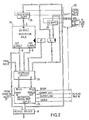
- FIG. 3 A typical multiple-processor system configuration incorporating a plurality of substantially identical processing units in accordance with the invention is shown in Fig 3, illustrating the manner in which the processing units can be interconnected to perform complex signal processing problems requiring computing power greater than that which can be achieved using a single unit.
- the configuration starts at the top of the tree with a first processing unit PU1 whose master interface arrangement is connected by means of a data and address bus set to a host minicomputer (not shown) which controls the overall operation of the system via the top unit PU1.
- the host mini-computer need access only the status register 14 of PU1 in order to initiate and monitor its operation, although in practice it may also provide input and output of data to and from : the read/write memory of PU1,
- the slave interface arrangement of PU1 is in turn connected by a data and address bus network to the master interface arrangements of each of four slave processing units PU2 to PU5, and to an input/output (I/O) interface unit 60.
- PU1 may communicate with the I/O interface unit to load data into its own internal read/write memory 35, transfer data between the I/O interface unit and any one or all of its slave units CP2 to CPU, transfer data from its own read/write memory to that of any one or all of its slaves, or transfer data between any combination of its slaves via the data and address bus network.
- Writing of data into or reading of data from any of the slaves can only be done while the particular slave or idle.
- the same data and address bus network is used by PU1 to control and monitor the opereration of the slave units PU2 to PU5 by addressing their status registers.
- the slave unit PU5 is itself connected to an I/O interface unit 61, and its own set of three slaves PU6 to PU8, and the same considerations regarding control, monitoring and inter-communications apply.
- the third of these slaves PU8, has its slave interface unit connected to an external memory 63 effectively providing the system with an increased memory workspace.
- the size of this memory may be as large as the 16-bit address word capability of its slave interface arrangement will allow, ie 64K words.
- this memory space may alternatively be provided by a part of the externally accessible read/write memory area provided in the example by the read/write memory 35.
- This part of the internal read/write memory may then be accessed frcm outside via the master interface arrangement, for the purpose of writing control instructions to, and for monitoring the status of,the processing unit.
- the control section will also be able to access this part of the internal read/write memory for the purpose of reading control instructions previously written into it from outside, and writing into it data relating to the operating status of the processing unit for mcnitoring purposes.
- communications to and between processing units for these control and monitor purposcs may be effected by a separate control bus arrangement.
- Each processing unit will then have a separate interface arrangement solely for use in transmitting control instructions to, and receiving data relating to the operating status of, any slave processing units to which it is connected; and for receiving control instructions from and transmitting data relating to its operating status to, its controller, eg its master processing unit.
Abstract
Description
- This invention relates to digital data processing apparatus.
- The invention is particularly though not exclusively concerned with digital data processing apparatus suitable for special purpose signal processing applications in which the amount of computing power is substantially more than can be obtained from a single bit-slice central processing unit (CFU).
- It is accepted that considerable savings in the cost and size of high power special purpose signal processors could be achieved if it were possible to effectively use current highly integrated components such as bit-slice CFUs. The reason for this is that these more highly integrated components are considerably cheaper per gate than the medium and large scale discrete integrated circuit combinations from which special purpose hardware signal processors are usually constructed, even allowing a substantial factor for inefficiency in using those gates. On the other hand, a special purpose signal processor is almost inevitably more efficient in dealing with signal processing problems than a general purpose computer, because the latter incurs speed penalties in the serial nature of its operations and fairly high hardware overheads because of its generality (eg the need to be able to store and load programs).
- However, difficulties do arise in the use of highly integrated components such as bit-slice CPU devices in any application where the amount of computing power is substantially more than can be obtained from a single CPU device. The main difficulty is in the definition of an architecture in which a number of such devices can co-operate to produce the necessary computing power without high overheads or complex operating systems. There are also associated practical difficulties of programming a complex multiple processor system and in maintaining the system when constructed.
- It is an object of the present invention to provide means whereby at least some of the above-mentioned disadvantages may be overcome or at least substantially reduced.
- According to the present invention, a data processing unit comprises:
- a control section responsive to a control instruction to switch the processing unit from an idle mode to an execution mode, the control section being operative during the execution mode to initiate and control the sequence of execution of a program stored therein and to automatically switch the processor unit to the idle mode when execution of the program is completed;
- a memory section including an area of read/write memory;
- a computation section for performing calculations in accordance with instructions from the program and capable of accessing the read/write memory area during execution of the program;
- and interface means through which the processing unit can access an external memory when in its execution mode, through which at least part of the read/write memory area of processor unit can be accessed when in its idle mode, and. through which an instruction for switching the processing unit from its idle to its execution mode can be received.
- Thus, data on which the processing unit is to perform its computations in accordance with the program stored in its control section may be loaded into the read/write memory area from outside via the interface means when the processing unit is idle prior to initiation by the start instruction. In the course of execution of the program, this data may be read from the read/write memory area by the control section, and calculations performed on it before the "answer" is written back into the read/write memory area. In the course of executing the program, the processing unit may also access an external memory via its interface means either to write data into it or to read data from it. When the processor unit has completed execution of the program, and is switched to its idle mode, the internal read/write memory may then be accessed from outside, via the external bus system, eg to recover the "answer" .Alternatively, the processing unit may write the data into an external memory before switching to its idle mode.
- Because a processing unit in accordance with the. invention can both access an external memory when in its execution mode, and have its read/write memory area accessed when in its idle mode, the interface units of two such processing units may be connected together so that one of them, when in its execution mode, can access the internal read/write memory area of the other when in its idle mode.
- The interface means may conveniently comprise a master interface unit for connecting the processing unit to an address bus through which the processing unit can receive address words designating locations in its internal read/write memory area, and to a data bus through which it can receive or transmit data to be written into or read from the memory locations designated by the address words; and a slave interface unit for connecting the processing unit to an address bus through which the processing unit can transmit memory addresses to an external memory area and to a data bus through which data to be written into or read from the external memory can be transmitted or received. Thus, the slave interface.unit of a first processing unit may be connected to the master interface unit of a second processing unit by means of data and address buses in such a way that the first processing unit when in execution mode can access the internal read/write memory of the second processing unit when the latter is idle. Similarly the slave interface unit of the second processor unit may also be connected to the master interface unit of a third processor unit such that the second processor unit when in its execution mode can access the internal read/write memory of the third processing unit when the latter is idle. Thus any number of processing units may be connected together in a chain configuration.
- Preferably, however, the external memory address capacity of the processing unit via its slave interface unit is substantially greater than the internal read/write memory address capacity that is accessible from outside: via its master interface unit, thereby enabling a number of processing units to be connected to the slave interface unit of a single processing unit.
- Preferably a part of said externally accessible internal read/write memory area is accessible also from the control section and is preferably provided by a separate memory device.
- This part of the internal read/write memory area provides means whereby control data for controlling the operation of the processor can be written into the processing unit from outside, and which can also be read by the control section to derive the start instruction and initiate execution of a program. Furthermore, it enables the processing unit to be directly controlled by another processing unit of the same kind via their respective interface units.
- Thus, if the slave interface unit of a first processing unit is connected to the master interface unit of a.second processing unit, the first processing unit can access, for the purpose of writing control data into the part of the internal read/write memory area of the second processing unit which is accessible also to the control section thereof. The first processing unit can thus control the second processing unit, and similarly any other processing units whose master interface units are connected to its slave interface unit.
- Preferably said part of the internal read write/ memory area which is accessible to the control section, is accessible both during the idle and the execution mode of the processing unit, and the control section includes means for writing into it data indicating a change in the activity status, idle or executing,of the processing unit. This enables the activity status of a first unit to be monitored by a second processing unit which has access to the internal read/write memory area. Furthermore it enables the second processing unit to write new control data into the first processing unit whether the latter is in its idle or execution mode. This facility may be used to effect switching of the first processing unit between its idle and its execution modes eg to allow the second processing unit to access the read/write memory area of the first processing unit when the latter is in the middle of a program execution.
- It will be apparent that the said part of the internal memory area which is accessible both to the control section and from outside via the(master) interface unit need only comprise a 1bit memory word, one value (eg '0') indicating the idle mode and the other (eg '1') indicating the execution mode. This one bit may be written or. read from outside for control and monitor purposes respectively; or written or read from inside by the control section on the one hand to provide an indication of the processor units activity status for external monitoring purposes, and on the other to enable the control section to respond to a change in the bit value to switch between modes.
- Preferably however, the control section is capable of controlling the execution of a plurality of programmes the sequential instructions of which are stored in a programmable read only memory (PROM) each having a different starting address in the PROM. In this case, the part of the internal read/write memory which is accessible both to the control section and from outside via the (master) interface unit will include, in addition to the above single status bit, address word bits into which the PROM start address for any one of the stored programs can be written from outside, and which can be read by the control section for program selection.
- Although a processing unit in accordance with the invention can be used on its own to perform data processing operations, and in particular signal processing operations, the purpose of the invention is to provide a modular processing unit which may be connected to cooperate with one or more other processing units of the same kind in carrying out complex data processing operations requiring computing power greater than that which can be achieved using a single processor unit. In designing a multiple processor system for such applications using a'number of processing units in accordance with the invention, each processing unit may be programmed to carry out a particular function, which function may include the designation of parts of that function to one or more other processing units and the control of those processing units in performing their particular functions. In addition, any of the processing units in the system may be given access, by means of its (slave) interface means, to external memory or input/output devices for example, to provide resources not available from the combination of several processors. The processing unit can access these other devices in the same way as it accesses the internal memories of other processing units.
- The invention will now be described in greater detail, by way of example only, with reference to the accompanying drawings, of which:
- Figure 1 is a block schematic diagram of a processor unit in accordance with the present invention:
- Figure 2 is a block schematic diagram of part of the processor unit of Figure 1, and
- Figure 3 is a block schematic diagram of processor system incorporating a plurality of processor units of the kind shown in Figure 1.
- Referring now to Figure 1 of the drawings the processor unit is divided for convenience into three sections separated in the drawing by broken lines. These sections comprise a
control section 1, containing a microcode memory in which one or more micro-programs which determine the function or functions of the processor unit are stored; amemory section 2 containing an area of read/ write memory for storing variable data and an area of programmable read only memory (PROM) in which fixed data tables, such as sine and coscine look-up tables, can be stored; and acomputation section 3 in which the mathematical data, memory address, and loop counting computations are performed in accordance with instructions from the microprogram. - The processor unit is also provided with two interface arrangements for connection to respective sets of data and address buses. The first of these interface arrangements, which will hereinafter be referred to as the slave interface arrangement (44,45) can be used to connect the processing unit to one or more other processing units of the same kind, to enable it to access the memory sections of, and to monitor and control the operation of those other (slave) processing units. This slave interface arrangement may also enable the processing unit to be connected to external memories or I/O latches.
- The second of the interface arrangements, which will hereinafter be referred to as the master interface arrangement (42,43), enables the processing unit to be monitored and controlled, and have part of its internal memory section accessed from outside, eg from another (master) processor unit of the same kind. This is achieved by connecting the master interface arrangement of the processing unit to the slave interface arrangement of this other (master) processing unit.
- Thus, a number of processor units may be connected together in master/slave relationships to form a 'tree' structure by interconnecting the master interface arrangements of some of the processing units with the slave interface arrangements of others as illustrated schematically in Figure 3. As indicated earlier, a number of processing units may be connected as slaves to a common master, but a slave processing unit will normally be connected to only one master processing unit. Furthermore, a processing unit which is connected as a slave to a master processing unit may also be connected as a master to one or more slave units.
- The data and address bus set which interconnects the slave interface arrangement of a master processing unit with the master interface arrangement of each of its slave processing units enables it to monitor the operation of the slave to determine whether it is idle or whether it is executing a program, these being the only two modes of which a processing unit is capable. The same data and address bus set also enables the master processing unit to independently switch any one of its slave processing units from its idle to its execute mode, ie to start the slave unit, or to switch it from its execute to its idle mode, ie to stop the slave unit. When switching from idle to execute, the master may also select which of the slave's microprograms is to be executed. When the slave is in its idle condition, typically before it commences execution of a microprogramme or when it has completed execution of a microprogram on a particular block of data, the master may access the slave's internal memory section, either to write data into, or to read data from it. The data read from (or written into) the slave's memory section may be transferred to (or from) the master's own internal memory section, the internal memory section of another one or more of its slaves, or from an external memory or 1/0 latch to which the master's slave interface arrangement is connected.
- A typical sequence of operation would begin with a master in execution mode and its slaves idle. In this situation the master may write data into its slaves' memory sections, select appropriate programs within the slaves microcode memories, and then switch them to execution mode. The master may continue in execution mode and then monitor the status of its slaves until they have completed executicn of their respective programs on the data which was supplied to them, and again become idle. The master may then access the slaves' memory sections either to copy the results of slaves' computations into its own memory section, or to transfer intermediate data from one slave to another. While the slaves are in execution mode, they may themselves become masters controlling their own slaves at the next level down in the tree structure.
- The top processing unit of the tree structure will normally be connected to a host minicomputer which will thus have overall control of the whole multiple-processor system, and be able to supply input data to, and read output data from, the system via this top processing unit. Additionally input/output of data may be achieved by means of I/O latches connected at appropriate locations within the tree structure.
- .Thus a processing unit may either be used on its own, or a complex multiple processor system suitable for special purpose signal processing applications may be constructed from a number of identical processing units each adapted to perform a specific function or functions determined by its particular microprogram(s).
- A more detailed description of an individual processing unit in accordance with the invention will now be given with reference to Figures 1 and 2 of the accompanying drawings. For the purposes of this description it will be assumed that the processing unit is connected as one of a number of slaves to one other processing unit, and is connected as a master to a number of its own slave unit.
- The
control section 1 of the processing unit is built around a microcode memory in the form of a programmable read only memory 5 (PROM) of 1K, 72 bit wide micro-instruction words. Each micro-instruction word represents one step in a microprogram, of which up to 16 may be stored in the PROM, and is largely horizontally coded enabling the various parts of the processing unit to be operated in parallel as will be described below. - Under normal sequential program execution a 10-bit word latched in an
address register 6 and designating the address of a micro-instruction word in thePROM 5 is incremented by 1 each cycle so that the micro-instruction words of successive PROM addresses are executed in sequence, Incrementing of the 10-bit PROM address word is effected by an increment counter 7 which,in successive cycles,adds 1 to the numerical value of the address word of the preceding cycle held in theaddress register 6, and feeds the new address word back into it. - The processing unit is however capable of non- sequential program execution, in which a part of the micro-instruction word can be used to instruct the processing either to 'jump', 'call', 'return' or 'stop'. The 'jump' instruction overrides the increment counter 7 and causes a new 10-bit PROM address word, contained in the same 72-bit micro-instruction word as the 'jump' instruction itself, to be written into the
address register 6 so that the program continues normal sequential execution from the new address (at least until a further non- sequential instruction appears). The program may thus be made to 'jump' from and to any micro-instruction word stored in thePROM 5. - The 'call' instruction is used in conjunction with the 'return' instruction, and is similar to the'jump' instruction in that it causes the program to jump to a new micro-instruction word designated by a 10-bit PROM address word contained in the same micro-instruction word as that which executes the call instruction.The 'call' instruction, however, is always followed at some later stage in the program sequence by a 'return' instruction which causes the program to return to the micro-instruction word succeeding that which contained the original 'call' instruction. Thus, when a 'call' instruction is executed, the 'return' address is taken from the increment counter 7 and is stored in a stack 8 (last-in-first-out buffer) which will allow the nesting of return addresses up to 4 deep. Thus up to three additional 'call' and 'return' instructions may be executed between the first occuring 'call' instruction and its associated 'return' instruction.
- Finally, the fourth program instruction which may be used to alter the normal sequential operation of the program is the 'stop' instruction which simply changes the operating mode or status of the processor unit from running to idle, following which its
memory section 2 may be accessed from outside as discussed earlier. - Excution of each of the four sequence-control instructions described above may be conditional upon the value of.a 1-
bit flag register 16, the conditionality being determined by one bit in the micro-instruction word. - The
control section 1 of the processing unit also includes control logic circutry 9, and aclock control unit 10. - The
clock control unit 10 is controlledviaaclock line 12, by the clock control unit of its master processor unit, and the clock control units of its slave units are controlled by thecontrol unit 10 viaclock line 13. Theclock control unit 10 determines the cycle time of the processing unit via the control logic circuit 9. - The control logic circuitry 9 also performs several other functions. It is used to override any one of the four sequence control instructions when such instructions are conditional upon the value of the 1-
bit flag register 16 and when the flag register bit is set at '0'. It also provides thecontrol section 1 with access to a status register 14 which effectively forms part of thememory section 2 of the processing unit, and which is accessible also from outside via the master interface arrangement. The status register 14 provides the means whereby the operation of the processing unit can be controlled and monitored from outside eg by its master processing unit, and contains 6 bits, S1 to S6 as follows:


- Before initiation of a program, ie while the processing unit is idle and bit S1 reads '0', the 4-bit PROM address of the first micro-instruction word of the program is written by the master processing unit into
bits S3 5. to S6 of the status register 14 (the PROM may thus contain up to 16 microprograms having start addresses 1 to 16 respectively) and sets bit S1 to '1' to initiate execution of the program. The control logic circuitry will then respond to the change in the status bit S1 from '0' to '1' to begin execution of the program reading its first PROM instruction address from bits S3 to S6 into theaddress register 6. The master unit may then poll the status bit S1 until it is cleared to '0' by the control logic circuitry 9 upon execution of a 'stop' instruction in the microprogram. - The master may also stop execution of the program at any time by clearing
bit S1 to '0', eg to enable it to access
thememory section 3 of the processor unit as will be described later. - Bit S2 enables the master to control a distribution mode of transfer either from the master to all slaves which have their S2 bits set at '1', or from one slave to any of the other slaves which have their S2 bits set at '1' as will also be discussed later.
- The internal operation of the
control section 1 is determined by 17 bits (P1 to P17) of each micro-instruction word as follows. The first bit, P1, determines the interpretation of bits P2 to P17 as either a data word or as a sequence control instruction.
- If P1 in the micro-instruction word is '1' then P2 to P15 consists of a sequence control instruction which controls the processor operation as follows:


- Alternatively, if P1 is '0' in the micro-instruction word, then P2 to P17 consists of a 16-bit data constant word which is latched into
register 17 to provide a constant for thecomputation section 3. - The remaining bits of the micro-instruction word, bits P18 to P72 are latched into a
register 20 and used to control various parts of the memory and computation sections of the processor unit via internal control lines (not shown). - The
computation section 3 of the processor unit is controlled by bits P18 to P68 of the micro-instruction word and includes two computational units designated CPU-A and CPU-B in Figure 1. CPU-A provides the main computational unit in which most of the mathematical data calculations are performed, while CPU-B is used only for address calculations and loop counting. Both CPUs are constructed from identical commercially available 4 x 4-bit (ie operating on 16-bit words) CPU slices fabricated using large scale integration (LSI) microprocessor technology. The CPUs described here and shown in Figure 2 by way of example are type Am 2901 manufactured by Advanced Micro Devices Inc., of Sunnyvale, California, USA. - The computation section also includes a
multiplication unit 22 for performing multiplications, and ascale accumulation unit 23 which enables a check to be maintained on the data being transferred into thememory section 2. This gives warning of close-to-overflow conditions, enabling preventive scaling to be done when the data is next accessed. A number of registers D,R,Y,Z, and W are also provided for routing data between various parts of thecompution section 1 and thememory section 3. - Figure 2 shows the main computation unit, CPU-A, in greater detail, and it includes a
file 24 of 16 general purpose 16-bit registers and two special purpose registers Q and ø the latter of which simply provides the operand zero. - The register file has two outputs a and b through which the contents of any two registers of the file designated a reg and b reg may be read, and one input d through which data may be read into the register (b reg) associated with output b. The two 4-bit addresses which specify these two registers a reg, b reg are contained in the micro-instruction word.
- CPU-A also includes an arithmetic/
logical unit 25 which takes two operands x,y, selected by an operandselect unit 26 from various sources determined by bits of the micro-instruction word, and performs on them add, subtract and logical operations again determined by the micro-instruction word, to produce a function result f. The sources from which the operandselect unit 26 may select the two operands x,y are the two output registers a reg, b reg of theregister file 24, register 0, register Q, and the external register D through which all input data enters CFU-A. - In addition to the output function f, the arithmetic/
logical unit 25 also makes available four status bits designated SIGN, CARRY-OUT, OVERFLOW and ZERO for storage in theflag register 16 of thecontrol section 1. The SIGN status bit indicates the sign (+ or - in two's complement notation) of the output function value f; the CARRY-OUT bit is the carry bit resulting from an addition or subtraction operation; the OVERFLOW bit is the bit produced in the event of an overflow condition resulting from an arithmetic operation, and the ZERO bit indicates a zero value for the OUTPUT function f. - The arithmetic/
logical unit 25 is also associated with a carry-inselect circuit 27 which is used to select a carry-in bit, eg the CARRY-OUT or OVERFLOW status bit, from theflag register 16 when appropriate for add and subtract operations thus enabling multi-word arithmetic operations to be performed. - Also included in CPU-A are two
shift networks shift control unit 30. Theshift network 28 is for performing 1-bit left or right shifts in the data word (output function f)being entered into the selected input register b reg of the register file, and theshift network 29 is for performing 1-bit left or right shifts in the data word stored in register Q. Theshift control unit 30 determines which bits are to be shifted in, and makes the bits shifted out available for storage in theflag register 16. - The output word from the CPU-A is selected by an output
select unit 31 from either the output function f of thearithmetic logic unit 25, or the first output register a reg of theregister file 24. The output function f from thearithmetic logic unit 25 may also be wri-tten into the input register b reg of theregister file 24, or the register Q, or both. - The operation of the various parts of CPU-A described above are controlled by a total of 20 bits, P18 to P37, from the micro-instruction word. The first 8 of these bits determine the two register file addresses as follows:


- The next three bits control the selection of the two operands x and y for the arithmetic/
logical unit 25 in accordance with one of the following eight combinations:
- The carry-in bit (c) to the arithmetic/logical unit is selected by the next bit:

logical unit 25 as follows:
x denotes the bit-complement of x, xor is the exclusive-or operation, and xor gives the bit-complement result of xor. - The next three bits of the micro-instruction word control the shift operations of the two
shift networks 
- As mentioned above, the shift-out bits are made available for storage in the
flag register 16, while the shift-in bit (the same bit for the f shift associated with the input d to register b reg and the register Q) is determined as follows:
- The sign of f shift-in bit is derived from the SIGN status bit produced by the arithmetic/
logical unit 25. - The second computational unit, CPU-B in Figure 1 is substantially identical to CPU-A shown in Fig 2, but only a subset of the functions are used. Its 16 general purpose registers in its register file are all available, but its register Q is ignored, as are the shift networks and the carry-in-select, and the arithmetic/logical unit is restricted to add and subtract functions only.
- CPU-B takes its input from the register Z which in turn takes as its input the output word from CFU-A, either directly or via a patch field which may be wired specially to provide a 16-bit permutation of the data. Its output word is used for memory addressing in the same instruction cycle as the address is calculated.
- The operation of CPU-B is controlled by 12 bits of the micro-instruction word, P38 to P49. The first 8 bits provide the two register file addresses, i reg, j reg


- The next bit P48, determines which of two functions is to be performed by the arithmetic/logical unit on the two operands, and bit P49 determines the CPU-B output word (always the output function g of the arithmetic/logical unit) and the destination of the output function g.


- The
multiplication unit 22 takes two 16-bit signed input words in two's complement notation from the registers Y and W respectively, and calculates a 32-bit signal product. A 16-bit result is selected from the bit product as follow. Two standard selectiorsare provided: the least significant 16 bits (bits 0 to 15) and the most significant 16 bits (bits 16 to 31), Two additional selections may be made using apatch field 32 specially wired as required. The facility is also provided for automatic rounding of the 16-bit result by adding a '1' in the appropriate bit position (eg bit 15 for the most significant 16 bits result). - The selected 16 bit result from the multiplication unit is written into register R and may then be transferred in a subsequent instruction cycle to register D for processing in CPU-A.
- The operation of the
multiplication unit 22 is controlled by 4 bits, P50 to P53, of the micro-instruction word as follows:


- The
scale accumulation unit 23 is provided to maintain a check on the most significant bits of data being written from the register Y to thememory section 2. The register Y may receive data either from CPU-A or from an internal data bus 33 (shown as a solid bus line in Fig 1) which also provides a source of data for the register D and thescale accumulation unit 23. The data on the internal bus may itself come either from theregister 17, which provides a constant for the computation section, or from thememory section 2 of the processor unit. - The purpose of the
scale accumulation unit 23 is to warn of close-to-overflow conditions enabling preventive scaling to be effected when the data is next accessed. The unit contains two 6-bit mask register (not shown) in which two different threshold values derived from the low-order 12 bits of the 16-bit data word on theinternal data bus 33 taken from theconstant register 17, are stored. The threshold value stored in the first mask register corresponds to thehigh order 6 bits (bits 15 to 10) of the data word being transferred from the register Y to thememory section 2, while that stored in the second mask register corresponds to bits 14 to 9. The two 6-bit data word values are each compared with the appropriate 6 bit threshold value to produce respective status bits indicating whether the values of the data word bits are above or below their threshold values. The two status bits are made available for storage in theflag register 16 and can be used to indicate whether the data word value lies above the higher threshold value, below the lower threshold value or between the two threshold values. - The unit operates in two modes, one for signed data and one for unsigned data. In the unsigned mode, the operation for each mask register is as follows: the 6 bits of the mask are ANDed with the appropriate 6 bits of the data word to produce a 6-bit result, and these 6 bits are then ORed together and with the corresponding existing status bit to give a new status bit. Thus the status bits are updated although the mask register values remain unchanged. In the signed mode, the bits of the data are first XORed with the sign bit and then operation continues as for the unsigned mode.
- The operation mode, signed or unsigned, is determined by an initialisation instruction contained in the micro-instruction word. At initialisation, the two status bits are cleared and the two mask registers load.ed from the
internal data bus 33. Subsequent updating of the status bits in the selected mode is effected by an 'update enable' instruction from the micro-instruction word. The instructions controllinE thescale accumulation unit 23 are contained in bits P54, P55 of the micro-instruction word as follows:
- The next 13 bits, P56-P68, of the micro-instruction word control the routing of data and various status bits between various parts of the register. In particular they control the source and destination of data and status bits which are written into or read out of a number of registers, namely registers D,Y,Z,W and the flag register. They also control the source and destination of data entered onto the
internal data bus 33. Data may be entered onto the internal bus either from theconstant register 17, the processor units internal memory or from an external memory via a register I. - The
flag register 16, and registers D,Y,Z and W are controlled by clock bits and select bits from the micro-instruction word, the clock bits determining whether a register retains its current value, or has new data clocked into it and the select bits determine which data is entered. - The micro-instruction word controls the above registers and internal data bus as follows:


- The
memory section 2 of the processor unit includes an internal read/write memory 35 of 4K words (address range 0 to 4095) for storing variable data, and aPROM 36 also of 4K words (address range 4096 to 8191) for storing data constants and tables, eg sine and cosine values. This section of the processor unit also includes the above-mentioned master interface arrangement, comprising a master data bus receiver/transmitter 42 and a masteraddress bus buffer 43, and the slave interface arrangement comprising a slave data bus receiver/transmitter 44 and a slaveaddress bus buffer 45. - When the processor unit controls one or more slave units, its slave data bus receiver transmitter and its slave address bus buffer are connected respectively by means of a 16-bit
slave data bus 46 and a 16-bitslave address bus 47, to the master data bus receiver/transmitter and the master address bus buffer of each slave. Similarly, when the processor unit is itself a slave unit (it may also be a master controlling its own slave units), its master data bus receiver/transmitter 42 and its masteraddress bus buffer 43 are connected respectively, by means of a 16-bitmaster data bus 48 and a 16-bitmaster address bus 49, to the slave data bus receiver/transmitter and the slave address bus buffer of its master. - The
internal memories latch register 38 by the output word of CPU-B. The output word of CPU-B may also be used to address the internal read/writememories 35 of any slave units (or other external memories to which it is connected) via the slaveaddress bus buffer 45 andslave address bus 47. Data read from either of theinternal memories internal data bus 33. Data being written into the read/write membry 35 (data cannot be whritten into the PROM 36) derives either from the register Y or from outside, eg from the master processing unit or another external membry via themaster data bus 48 and master data bus receiver/transmitter 42. Data from either of these sources is transmitted to the internal read/write memory via a multiplexer 39 andlatch register 40. - The memory address operation is controlled by a single bit, P69, of the micro-instruction word as follows:

- Thus a read operation is always performed, although the data read may or may not be selected for entry onto the
internal data bus 33 according to micro-instruction word bits P63,P64. When the write operation is enabled, this is done after a read operation so that in a read and write instruction, the data read is the old contents of the memory address. - In communications between a master and its slaves, the top 4 bits of the 16-bit
slave address bus 47 are used to designate a particular slave (there may therefore be up to 16 slaves connected to one master) and the appropriate slave unit recognises these 4 bits in anaddress decode unit 50 associated with its masteraddress bus buffer 43. The remaininglow order 12 bits of theslave address bus 47 determine the address in the slave's internal read/write memory 35 (the master cannot access a slave's PROM 36). Thus, the internal read/write memories of up to 16 slave units appear as a single external address space of up to 64K words (16 x 4K words read/write memory). - Data may either be written into or read from the selected address in a slave's read/write memory, via the
slave data bus 46, but this may only be done when the slave is idle, ie when bit S1 of its status register 14 is '0'. A slave's status register 14 may however be accessed at any time for monitor and control purposes. When accessing a. slave's status register the same 16-bit slave data andslave address buses low order 6 bits of the slave data bus (corresponding to the 6 bits of the status register) are relevant. - A distribute function is provided for writing the same data unit into several slave's read/write memories simultaneously (at the same address in each). When the distribute function is specified by the micro-instruction word of the master processor unit (discussed below) all slaves having their status register S2 bits set at '1' will accept data regardless of the top 4 bits on the master's slave address bus 47 (which is connected to the
master address buses 49 of its slaves). - Control of the master/slave communications is determined by bits P70 to P72 of the micro-instruction word as follows:

- Each of these communications functions actually takes two operating cycles to complete.
- In a master-to-slave write operation, the data, taken from the master's register Y, and the address, taken from CPU-B, are sent in
cycle 1 to the slave a.cross the mastersslave data bus 46 andslave address bus 47 respectively, and enter the slave via the slave's master databus receivers transmitter 42 and masteraddress bus buffer 43. Incycle 2 the slave uses the data and address to perform the write into its read/write memory 35 or status register 14 as appropriate. - In a master/slave read operation, the address from CPU-B of the master is sent to the slave's master
address bus buffer 43 across the master'sslave address bus 47 incycle 1. Incycle 2 the slave uses the address to read the data from its internal read/write memory 35, enters it on theinternal data bus 33 and transfers it to the master via its master data bus receiver/transmitter 42 andmaster data bus 48. The data arrives at the master's register I, via its slave data bus receiver/transmitter 44, early enough incycle 2 to be selected for entry onto the master'sinternal data bus 33 according to bits P63,P64 of its micro-instruction word. - A slave's status register 14 may similarly be read by a master using the same data and address buses.
- It will be seen that a potential clash in use of the master-to-
slave data bus 46 when a read instruction to a slave is immediately followed by a write instruction. This clash is resolved by giving the outgoing write data precedence over the incoming read data from the slave. Thus, the read data is lost, resulting in the master's register I containing the write data which is then entered.onto the internal data bus as for a normal read operation. - Since the internal and external (communications) memory functions can be carried out simultaneously, it is possible for block transfers of data (ie groups of data words) between a master and slave(s) to be performed at the rate of one data word per instruction cycle.
- For block transfer of data from master to slave(s) a data word (N) is read from an address (u) in the read/
write memory 35 of the master specified by the output word of its CPU-B, and routed to its register Y in the first cycle. In the second cycle a new address (u+1) is generated by the master's CPU-B and used to read out another data word (N+1) from the master'smemory 35 which is transferred to the master's register Y as before. Also during the second cycle, the data word N from the register Y is transmitted to the slave(s) together with the new address word (u+1) and is written into the read/write memory 35 of the slave(s) at an address word (u+1). Thus, the destination in the slave(s) is offset by one from the master's source address. - For block transfer of data from slave to master, the slave's address is sent to the slave in one cycle, the data from that address returns to the master's register I then Y in the next cycle, and is written into the master's memory in the third cycle. Again, as these 3 cycle operations overlap, the net result is that the destination address in the master is offset by two from slave's source address.
- Block transfer of data from one slave to other slaves may also be effected using the read and distribution functions. Data is read from a read/write address in the slave specified by the top 4-bits on its
master address bus 49 in one cycle, and written into the same address in the read/write memories of all slaves which have their status register 52-bits set at '1 in the following cycle. The destination address is offset by one from the source address. - Thus each processing unit is responsive on receipt of a single starting instruction entered into its status register 14 to perform the execution of a stored microprogram selected by the starting instruction. The activity status, idle or executing can be continuously monitored from outside to ascertain when the unit has completed execution of the program, following which results of its computations can be recovered from it. While executing the program, the processing unit may control and monitor, and access and transfer data between the internal read/write
memories 35 of, its slave processing units. Thus, a processing unit, in execution of a program, may delegate functions to each of its slaves by transferring data to their read/write memories, initiating their program execution on that data, and then recovering the results of those computations when completed. - A typical multiple-processor system configuration incorporating a plurality of substantially identical processing units in accordance with the invention is shown in Fig 3, illustrating the manner in which the processing units can be interconnected to perform complex signal processing problems requiring computing power greater than that which can be achieved using a single unit.
- The configuration starts at the top of the tree with a first processing unit PU1 whose master interface arrangement is connected by means of a data and address bus set to a host minicomputer (not shown) which controls the overall operation of the system via the top unit PU1. The host mini-computer need access only the status register 14 of PU1 in order to initiate and monitor its operation, although in practice it may also provide input and output of data to and from : the read/write memory of PU1,
- The slave interface arrangement of PU1 is in turn connected by a data and address bus network to the master interface arrangements of each of four slave processing units PU2 to PU5, and to an input/output (I/O)
interface unit 60. When in its execution mode, PU1 may communicate with the I/O interface unit to load data into its own internal read/write memory 35, transfer data between the I/O interface unit and any one or all of its slave units CP2 to CPU, transfer data from its own read/write memory to that of any one or all of its slaves, or transfer data between any combination of its slaves via the data and address bus network. Writing of data into or reading of data from any of the slaves can only be done while the particular slave oridle. The same data and address bus network is used by PU1 to control and monitor the opereration of the slave units PU2 to PU5 by addressing their status registers.
- In the same manner as PU1 is connected to slaves PU2 to PU5, and to the I/
O interface unit 60, the slave unit PU5 is itself connected to an I/O interface unit 61, and its own set of three slaves PU6 to PU8, and the same considerations regarding control, monitoring and inter-communications apply. The third of these slaves PU8, has its slave interface unit connected to anexternal memory 63 effectively providing the system with an increased memory workspace. The size of this memory may be as large as the 16-bit address word capability of its slave interface arrangement will allow, ie 64K words. - While it has been found convenient to use a separate memory device, ie the status register 14, to provide the means whereby the processing unit can be controlled and monitored from outside, this memory space may alternatively be provided by a part of the externally accessible read/write memory area provided in the example by the read/
write memory 35. This part of the internal read/write memory may then be accessed frcm outside via the master interface arrangement, for the purpose of writing control instructions to, and for monitoring the status of,the processing unit. In such an arrangement, the control section will also be able to access this part of the internal read/write memory for the purpose of reading control instructions previously written into it from outside, and writing into it data relating to the operating status of the processing unit for mcnitoring purposes. - Furthermore, communications to and between processing units for these control and monitor purposcs may be effected by a separate control bus arrangement. Each processing unit will then have a separate interface arrangement solely for use in transmitting control instructions to, and receiving data relating to the operating status of, any slave processing units to which it is connected; and for receiving control instructions from and transmitting data relating to its operating status to, its controller, eg its master processing unit.
Claims (15)
Applications Claiming Priority (2)
| Application Number | Priority Date | Filing Date | Title |
|---|---|---|---|
| GB7905022 | 1979-02-13 | ||
| GB7905022 | 1979-02-13 |
Publications (2)
| Publication Number | Publication Date |
|---|---|
| EP0016523A1 true EP0016523A1 (en) | 1980-10-01 |
| EP0016523B1 EP0016523B1 (en) | 1984-09-26 |
Family
ID=10503162
Family Applications (1)
| Application Number | Title | Priority Date | Filing Date |
|---|---|---|---|
| EP80300355A Expired EP0016523B1 (en) | 1979-02-13 | 1980-02-06 | Data processing unit and data processing system comprising a plurality of such data processing units |
Country Status (4)
| Country | Link |
|---|---|
| US (1) | US4376973A (en) |
| EP (1) | EP0016523B1 (en) |
| CA (1) | CA1135868A (en) |
| DE (1) | DE3069249D1 (en) |
Cited By (2)
| Publication number | Priority date | Publication date | Assignee | Title |
|---|---|---|---|---|
| EP0057511A1 (en) * | 1981-01-13 | 1982-08-11 | Nec Corporation | Information processing unit |
| EP0226096A2 (en) * | 1985-12-13 | 1987-06-24 | ELSAG BAILEY S.p.A. | Multiple-hierarchical-level multiprocessor system |
Families Citing this family (22)
| Publication number | Priority date | Publication date | Assignee | Title |
|---|---|---|---|---|
| US4736319A (en) * | 1985-05-15 | 1988-04-05 | International Business Machines Corp. | Interrupt mechanism for multiprocessing system having a plurality of interrupt lines in both a global bus and cell buses |
| JPH067380B2 (en) * | 1985-08-30 | 1994-01-26 | 株式会社日立製作所 | Multiprocessor system |
| US5036453A (en) * | 1985-12-12 | 1991-07-30 | Texas Instruments Incorporated | Master/slave sequencing processor |
| AU597980B2 (en) * | 1986-05-30 | 1990-06-14 | Honeywell Bull Inc. | Apparatus and method for interprocessor communication |
| US5140680A (en) * | 1988-04-13 | 1992-08-18 | Rockwell International Corporation | Method and apparatus for self-timed digital data transfer and bus arbitration |
| US4912633A (en) * | 1988-10-24 | 1990-03-27 | Ncr Corporation | Hierarchical multiple bus computer architecture |
| CH677047A5 (en) * | 1988-12-16 | 1991-03-28 | Asea Brown Boveri | |
| US5408627A (en) * | 1990-07-30 | 1995-04-18 | Building Technology Associates | Configurable multiport memory interface |
| IT1268611B1 (en) * | 1994-09-30 | 1997-03-06 | Finmeccanica Spa | COPROCESSOR FOR CHARACTER RECOGNITION |
| JP3123413B2 (en) * | 1995-11-07 | 2001-01-09 | 株式会社日立製作所 | Computer system |
| AU6495299A (en) * | 1998-09-18 | 2000-04-10 | Computron | Multiple operating system controller for a computer |
| JP2001224003A (en) * | 2000-02-10 | 2001-08-17 | Canon Inc | Terminal and its control method |
| EP1442359A4 (en) * | 2001-10-01 | 2007-12-26 | Benjamin Cooper | General purpose fixed instruction set (fis) bit-slice feedback processor unit/computer system |
| US7222251B2 (en) * | 2003-02-05 | 2007-05-22 | Infineon Technologies Ag | Microprocessor idle mode management system |
| US7826379B2 (en) * | 2005-02-07 | 2010-11-02 | International Business Machines Corporation | All-to-all sequenced fault detection system |
| US7437595B2 (en) * | 2005-02-07 | 2008-10-14 | International Business Machines Corporation | Row fault detection system |
| US7506196B2 (en) * | 2005-02-07 | 2009-03-17 | International Business Machines Corporation | System and method for detecting a faulty object in a system |
| US7529963B2 (en) * | 2005-02-07 | 2009-05-05 | International Business Machines Corporation | Cell boundary fault detection system |
| US7451342B2 (en) * | 2005-02-07 | 2008-11-11 | International Business Machines Corporation | Bisectional fault detection system |
| US7506197B2 (en) * | 2005-02-07 | 2009-03-17 | International Business Machines Corporation | Multi-directional fault detection system |
| US8495411B2 (en) * | 2005-02-07 | 2013-07-23 | International Business Machines Corporation | All row, planar fault detection system |
| CN100361118C (en) * | 2005-03-01 | 2008-01-09 | 华为技术有限公司 | Multiple-CPU system and its control method |
Citations (7)
| Publication number | Priority date | Publication date | Assignee | Title |
|---|---|---|---|---|
| US3219980A (en) * | 1960-06-30 | 1965-11-23 | Ibm | Computer multiplexing apparatus |
| DD101040A1 (en) * | 1972-12-28 | 1973-10-12 | ||
| US3962685A (en) * | 1974-06-03 | 1976-06-08 | General Electric Company | Data processing system having pyramidal hierarchy control flow |
| FR2329019A1 (en) * | 1975-10-24 | 1977-05-20 | Elsag | Real time modular micro processor - regulates data exchange from exchange parameters in programmable data system |
| US4064486A (en) * | 1975-05-29 | 1977-12-20 | Burroughs Corporation | Data communications loop synchronizer |
| US4096566A (en) * | 1974-12-27 | 1978-06-20 | International Business Machines Corporation | Modular signal processor having a hierarchical structure |
| AT354783B (en) * | 1978-02-07 | 1980-01-25 | Bruno Dr Buchberger | PROGRAMMABLE CIRCUIT FOR DATA PROCESSING |
Family Cites Families (12)
| Publication number | Priority date | Publication date | Assignee | Title |
|---|---|---|---|---|
| US3348210A (en) * | 1964-12-07 | 1967-10-17 | Bell Telephone Labor Inc | Digital computer employing plural processors |
| US3573736A (en) * | 1968-01-15 | 1971-04-06 | Ibm | Interruption and interlock arrangement |
| US3528062A (en) * | 1968-07-05 | 1970-09-08 | Ibm | Program interlock arrangement,including task suspension and new task assignment |
| US4558411A (en) | 1969-05-19 | 1985-12-10 | Burroughs Corp. | Polymorphic programmable units employing plural levels of sub-instruction sets |
| US4099241A (en) * | 1973-10-30 | 1978-07-04 | Telefonaktiebolaget L M Ericsson | Apparatus for facilitating a cooperation between an executive computer and a reserve computer |
| US4123794A (en) * | 1974-02-15 | 1978-10-31 | Tokyo Shibaura Electric Co., Limited | Multi-computer system |
| US3961312A (en) * | 1974-07-15 | 1976-06-01 | International Business Machines Corporation | Cycle interleaving during burst mode operation |
| US3962682A (en) * | 1974-10-30 | 1976-06-08 | Motorola, Inc. | Split low order internal address bus for microprocessor |
| US3941989A (en) * | 1974-12-13 | 1976-03-02 | Mos Technology, Inc. | Reducing power consumption in calculators |
| IT1047329B (en) * | 1975-09-30 | 1980-09-10 | C Olivetto E C S P A Ing | REMOTE IGNITION AND INITIALIZATION DEVICE OF A TERMINAL |
| DE2641741C2 (en) * | 1976-09-16 | 1986-01-16 | Siemens AG, 1000 Berlin und 8000 München | Computing system made up of several individual computers connected and interacting with one another via a manifold system and a control computer |
| US4149242A (en) * | 1977-05-06 | 1979-04-10 | Bell Telephone Laboratories, Incorporated | Data interface apparatus for multiple sequential processors |
-
1980
- 1980-02-06 EP EP80300355A patent/EP0016523B1/en not_active Expired
- 1980-02-06 DE DE8080300355T patent/DE3069249D1/en not_active Expired
- 1980-02-08 US US06/119,726 patent/US4376973A/en not_active Expired - Lifetime
- 1980-02-13 CA CA000345571A patent/CA1135868A/en not_active Expired
Patent Citations (7)
| Publication number | Priority date | Publication date | Assignee | Title |
|---|---|---|---|---|
| US3219980A (en) * | 1960-06-30 | 1965-11-23 | Ibm | Computer multiplexing apparatus |
| DD101040A1 (en) * | 1972-12-28 | 1973-10-12 | ||
| US3962685A (en) * | 1974-06-03 | 1976-06-08 | General Electric Company | Data processing system having pyramidal hierarchy control flow |
| US4096566A (en) * | 1974-12-27 | 1978-06-20 | International Business Machines Corporation | Modular signal processor having a hierarchical structure |
| US4064486A (en) * | 1975-05-29 | 1977-12-20 | Burroughs Corporation | Data communications loop synchronizer |
| FR2329019A1 (en) * | 1975-10-24 | 1977-05-20 | Elsag | Real time modular micro processor - regulates data exchange from exchange parameters in programmable data system |
| AT354783B (en) * | 1978-02-07 | 1980-01-25 | Bruno Dr Buchberger | PROGRAMMABLE CIRCUIT FOR DATA PROCESSING |
Non-Patent Citations (1)
| Title |
|---|
| LOBEL, MULLER, SCHMID "Lexikon der atenverarbeitung", 4th edition, 1969, VERLAG MODERNE INDUSTRIE, Munchen, page 364 * |
Cited By (3)
| Publication number | Priority date | Publication date | Assignee | Title |
|---|---|---|---|---|
| EP0057511A1 (en) * | 1981-01-13 | 1982-08-11 | Nec Corporation | Information processing unit |
| EP0226096A2 (en) * | 1985-12-13 | 1987-06-24 | ELSAG BAILEY S.p.A. | Multiple-hierarchical-level multiprocessor system |
| EP0226096A3 (en) * | 1985-12-13 | 1988-08-03 | Elettronica San Giorgio- Elsag S.P.A. | Multiple-hierarchical-level multiprocessor system |
Also Published As
| Publication number | Publication date |
|---|---|
| US4376973A (en) | 1983-03-15 |
| CA1135868A (en) | 1982-11-16 |
| DE3069249D1 (en) | 1984-10-31 |
| EP0016523B1 (en) | 1984-09-26 |
Similar Documents
| Publication | Publication Date | Title |
|---|---|---|
| EP0016523B1 (en) | Data processing unit and data processing system comprising a plurality of such data processing units | |
| CN110688157B (en) | Computing device and computing method | |
| JP3573755B2 (en) | Image processing processor | |
| US4314349A (en) | Processing element for parallel array processors | |
| US5099417A (en) | Data processing device with improved direct memory access | |
| US4891751A (en) | Massively parallel vector processing computer | |
| US5815723A (en) | Picket autonomy on a SIMD machine | |
| US5204938A (en) | Method of implementing a neural network on a digital computer | |
| US4131941A (en) | Linked microprogrammed plural processor system | |
| US4484303A (en) | Programmable controller | |
| US4912636A (en) | Data processing device with multiple on chip memory buses | |
| US3760369A (en) | Distributed microprogram control in an information handling system | |
| US3585605A (en) | Associative memory data processor | |
| US4229801A (en) | Floating point processor having concurrent exponent/mantissa operation | |
| JPH02300983A (en) | Fast arithmetic processing for central processing unit | |
| JPS6311697B2 (en) | ||
| GB1585284A (en) | Cpu/parallel processor interface with microcode extension | |
| Kartashev et al. | A multicomputer system with dynamic architecture | |
| JPS63278136A (en) | Arithmetic circuit | |
| CA1181865A (en) | Microprogrammed control of extended integer instructions through use of a data type field in a central processor unit | |
| US4792894A (en) | Arithmetic computation modifier based upon data dependent operations for SIMD architectures | |
| US5983328A (en) | Data processing device with time-multiplexed memory bus | |
| US5907864A (en) | Data processing device with time-multiplexed memory bus | |
| US4224668A (en) | Control store address generation logic for a data processing system | |
| JPS6226050B2 (en) |
Legal Events
| Date | Code | Title | Description |
|---|---|---|---|
| PUAI | Public reference made under article 153(3) epc to a published international application that has entered the european phase |
Free format text: ORIGINAL CODE: 0009012 |
|
| AK | Designated contracting states |
Designated state(s): DE FR GB NL |
|
| 17P | Request for examination filed |
Effective date: 19810317 |
|
| GRAA | (expected) grant |
Free format text: ORIGINAL CODE: 0009210 |
|
| AK | Designated contracting states |
Designated state(s): DE FR GB NL |
|
| REF | Corresponds to: |
Ref document number: 3069249 Country of ref document: DE Date of ref document: 19841031 |
|
| ET | Fr: translation filed | ||
| PGFP | Annual fee paid to national office [announced via postgrant information from national office to epo] |
Ref country code: NL Payment date: 19850228 Year of fee payment: 6 |
|
| PLBE | No opposition filed within time limit |
Free format text: ORIGINAL CODE: 0009261 |
|
| STAA | Information on the status of an ep patent application or granted ep patent |
Free format text: STATUS: NO OPPOSITION FILED WITHIN TIME LIMIT |
|
| PG25 | Lapsed in a contracting state [announced via postgrant information from national office to epo] |
Ref country code: DE Effective date: 19851101 |
|
| 26N | No opposition filed | ||
| PG25 | Lapsed in a contracting state [announced via postgrant information from national office to epo] |
Ref country code: NL Effective date: 19860901 |
|
| GBPC | Gb: european patent ceased through non-payment of renewal fee | ||
| NLV4 | Nl: lapsed or anulled due to non-payment of the annual fee | ||
| PG25 | Lapsed in a contracting state [announced via postgrant information from national office to epo] |
Ref country code: FR Free format text: LAPSE BECAUSE OF NON-PAYMENT OF DUE FEES Effective date: 19861031 |
|
| REG | Reference to a national code |
Ref country code: FR Ref legal event code: ST |
|
| PG25 | Lapsed in a contracting state [announced via postgrant information from national office to epo] |
Ref country code: GB Effective date: 19881118 |