DE10196442B4 - Electronic component comprising a dielectric film of at least one bis (4-mercaptophenyl) sulfide derivative - Google Patents
Electronic component comprising a dielectric film of at least one bis (4-mercaptophenyl) sulfide derivative Download PDFInfo
- Publication number
- DE10196442B4 DE10196442B4 DE10196442T DE10196442T DE10196442B4 DE 10196442 B4 DE10196442 B4 DE 10196442B4 DE 10196442 T DE10196442 T DE 10196442T DE 10196442 T DE10196442 T DE 10196442T DE 10196442 B4 DE10196442 B4 DE 10196442B4
- Authority
- DE
- Germany
- Prior art keywords
- monomer
- electronic component
- bis
- capacitor
- dielectric film
- Prior art date
- Legal status (The legal status is an assumption and is not a legal conclusion. Google has not performed a legal analysis and makes no representation as to the accuracy of the status listed.)
- Expired - Fee Related
Links
Images


Classifications
-
- C—CHEMISTRY; METALLURGY
- C07—ORGANIC CHEMISTRY
- C07C—ACYCLIC OR CARBOCYCLIC COMPOUNDS
- C07C323/00—Thiols, sulfides, hydropolysulfides or polysulfides substituted by halogen, oxygen or nitrogen atoms, or by sulfur atoms not being part of thio groups
- C07C323/10—Thiols, sulfides, hydropolysulfides or polysulfides substituted by halogen, oxygen or nitrogen atoms, or by sulfur atoms not being part of thio groups containing thio groups and singly-bound oxygen atoms bound to the same carbon skeleton
- C07C323/18—Thiols, sulfides, hydropolysulfides or polysulfides substituted by halogen, oxygen or nitrogen atoms, or by sulfur atoms not being part of thio groups containing thio groups and singly-bound oxygen atoms bound to the same carbon skeleton having the sulfur atom of at least one of the thio groups bound to a carbon atom of a six-membered aromatic ring of the carbon skeleton
- C07C323/19—Thiols, sulfides, hydropolysulfides or polysulfides substituted by halogen, oxygen or nitrogen atoms, or by sulfur atoms not being part of thio groups containing thio groups and singly-bound oxygen atoms bound to the same carbon skeleton having the sulfur atom of at least one of the thio groups bound to a carbon atom of a six-membered aromatic ring of the carbon skeleton with singly-bound oxygen atoms bound to acyclic carbon atoms of the carbon skeleton
-
- H—ELECTRICITY
- H01—ELECTRIC ELEMENTS
- H01C—RESISTORS
- H01C7/00—Non-adjustable resistors formed as one or more layers or coatings; Non-adjustable resistors made from powdered conducting material or powdered semi-conducting material with or without insulating material
- H01C7/003—Thick film resistors
- H01C7/005—Polymer thick films
-
- C—CHEMISTRY; METALLURGY
- C07—ORGANIC CHEMISTRY
- C07C—ACYCLIC OR CARBOCYCLIC COMPOUNDS
- C07C323/00—Thiols, sulfides, hydropolysulfides or polysulfides substituted by halogen, oxygen or nitrogen atoms, or by sulfur atoms not being part of thio groups
- C07C323/10—Thiols, sulfides, hydropolysulfides or polysulfides substituted by halogen, oxygen or nitrogen atoms, or by sulfur atoms not being part of thio groups containing thio groups and singly-bound oxygen atoms bound to the same carbon skeleton
- C07C323/11—Thiols, sulfides, hydropolysulfides or polysulfides substituted by halogen, oxygen or nitrogen atoms, or by sulfur atoms not being part of thio groups containing thio groups and singly-bound oxygen atoms bound to the same carbon skeleton having the sulfur atoms of the thio groups bound to acyclic carbon atoms of the carbon skeleton
- C07C323/12—Thiols, sulfides, hydropolysulfides or polysulfides substituted by halogen, oxygen or nitrogen atoms, or by sulfur atoms not being part of thio groups containing thio groups and singly-bound oxygen atoms bound to the same carbon skeleton having the sulfur atoms of the thio groups bound to acyclic carbon atoms of the carbon skeleton the carbon skeleton being acyclic and saturated
-
- C—CHEMISTRY; METALLURGY
- C08—ORGANIC MACROMOLECULAR COMPOUNDS; THEIR PREPARATION OR CHEMICAL WORKING-UP; COMPOSITIONS BASED THEREON
- C08F—MACROMOLECULAR COMPOUNDS OBTAINED BY REACTIONS ONLY INVOLVING CARBON-TO-CARBON UNSATURATED BONDS
- C08F22/00—Homopolymers and copolymers of compounds having one or more unsaturated aliphatic radicals each having only one carbon-to-carbon double bond, and at least one being terminated by a carboxyl radical and containing at least one other carboxyl radical in the molecule; Salts, anhydrides, esters, amides, imides or nitriles thereof
- C08F22/10—Esters
- C08F22/12—Esters of phenols or saturated alcohols
- C08F22/24—Esters containing sulfur
-
- H—ELECTRICITY
- H01—ELECTRIC ELEMENTS
- H01B—CABLES; CONDUCTORS; INSULATORS; SELECTION OF MATERIALS FOR THEIR CONDUCTIVE, INSULATING OR DIELECTRIC PROPERTIES
- H01B3/00—Insulators or insulating bodies characterised by the insulating materials; Selection of materials for their insulating or dielectric properties
- H01B3/18—Insulators or insulating bodies characterised by the insulating materials; Selection of materials for their insulating or dielectric properties mainly consisting of organic substances
- H01B3/30—Insulators or insulating bodies characterised by the insulating materials; Selection of materials for their insulating or dielectric properties mainly consisting of organic substances plastics; resins; waxes
- H01B3/301—Macromolecular compounds obtained by reactions forming a linkage containing sulfur with or without nitrogen, oxygen or carbon in the main chain of the macromolecule, not provided for in group H01B3/302
-
- H—ELECTRICITY
- H01—ELECTRIC ELEMENTS
- H01B—CABLES; CONDUCTORS; INSULATORS; SELECTION OF MATERIALS FOR THEIR CONDUCTIVE, INSULATING OR DIELECTRIC PROPERTIES
- H01B3/00—Insulators or insulating bodies characterised by the insulating materials; Selection of materials for their insulating or dielectric properties
- H01B3/18—Insulators or insulating bodies characterised by the insulating materials; Selection of materials for their insulating or dielectric properties mainly consisting of organic substances
- H01B3/30—Insulators or insulating bodies characterised by the insulating materials; Selection of materials for their insulating or dielectric properties mainly consisting of organic substances plastics; resins; waxes
- H01B3/44—Insulators or insulating bodies characterised by the insulating materials; Selection of materials for their insulating or dielectric properties mainly consisting of organic substances plastics; resins; waxes vinyl resins; acrylic resins
- H01B3/442—Insulators or insulating bodies characterised by the insulating materials; Selection of materials for their insulating or dielectric properties mainly consisting of organic substances plastics; resins; waxes vinyl resins; acrylic resins from aromatic vinyl compounds
-
- H—ELECTRICITY
- H01—ELECTRIC ELEMENTS
- H01C—RESISTORS
- H01C17/00—Apparatus or processes specially adapted for manufacturing resistors
- H01C17/06—Apparatus or processes specially adapted for manufacturing resistors adapted for coating resistive material on a base
- H01C17/065—Apparatus or processes specially adapted for manufacturing resistors adapted for coating resistive material on a base by thick film techniques, e.g. serigraphy
- H01C17/06506—Precursor compositions therefor, e.g. pastes, inks, glass frits
- H01C17/06573—Precursor compositions therefor, e.g. pastes, inks, glass frits characterised by the permanent binder
- H01C17/06586—Precursor compositions therefor, e.g. pastes, inks, glass frits characterised by the permanent binder composed of organic material
-
- H—ELECTRICITY
- H01—ELECTRIC ELEMENTS
- H01G—CAPACITORS; CAPACITORS, RECTIFIERS, DETECTORS, SWITCHING DEVICES OR LIGHT-SENSITIVE DEVICES, OF THE ELECTROLYTIC TYPE
- H01G4/00—Fixed capacitors; Processes of their manufacture
- H01G4/002—Details
- H01G4/018—Dielectrics
- H01G4/06—Solid dielectrics
- H01G4/14—Organic dielectrics
- H01G4/18—Organic dielectrics of synthetic material, e.g. derivatives of cellulose
Abstract
Elektronische Komponente, umfassend einen dielektrischen Film, der durch Ausbilden eines dünnen Filmes, welcher wenigstens einen Typ von Monomer enthält, und Polymerisieren des Monomers in dem dünnen Film, gebildet wird, wobei das Monomer eines oder eine Vielzahl von Monomeren umfasst, welche durch die allgemeine Formel 1 
die allgemeine Formel 4 
die chemische Formel 5 ![]()
the general formula 4
the chemical formula 5 ![]()

Description
Die vorliegende Erfindung betrifft eine elektronische Komponente mit meinem dielektrischen Film aus wenigstens einem Bis(4-mercaptophenyl)-sulfidderivat.The present invention relates to an electronic component comprising my dielectric film of at least one bis (4-mercaptophenyl) sulfide derivative.
Die
Die
Die
Herkömmlicherweise wurde ein Harzfilm als dielektrischer Film in einem Kondensator oder dergleichen verwendet. Ein solcher dielektrischer Film wird durch Bestrahlen eines auf einem Substrat abgeschiedenen Monomers mit Elektronenstrahlen oder Ultraviolettstrahlen zur Polymerisierung des Monomers ausgebildet, wie in
Elektronische Komponenten, welche die aus den oben beschriebenen Monomeren gebildeten dielektrischen Filme verwenden, weisen jedoch ein Problem dahingehend auf, dass die Eigenschaften bzw. Charakteristika nicht ausreichend sind. Insbesondere weisen elektronische Komponenten, welche die aus den oben beschriebenen Monomeren gebildeten dielektrischen Filme verwenden, das Problem auf, dass die Charakteristika unter hoher Feuchtigkeit und hoher Temperatur nicht ausreichend sind.Electronic components using the dielectric films formed from the above-described monomers, however, have a problem that the characteristics are not sufficient. In particular, electronic components using the dielectric films formed from the above-described monomers have the problem that the characteristics under high humidity and high temperature are insufficient.
Um das Problem zu lösen, ist es eine Aufgabe der vorliegenden Erfindung, eine elektronische Komponente, umfassend einen dielektrischen Film mit ausgezeichneten Eigenschaften bzw. Charakteristika unter hoher Feuchtigkeit und hoher Temperatur, bereitzustellen.In order to solve the problem, it is an object of the present invention to provide an electronic component comprising a dielectric film having excellent characteristics under high humidity and high temperature.
Gegenstand der vorliegenden Erfindung ist eine elektronische Komponente gemäß Anspruch 1. Bevorzugte Ausführungsformen ergeben sich aus den Unteransprüchen 2 bis 4.The present invention is an electronic component according to
Bei der elektronischen Komponente der vorliegenden Erfindung wird bevorzugt, dass das Monomer eines oder eine Vielzahl von Monomeren umfasst, welche durch die allgemeinen Formeln 1 und 4 und die chemischen Formeln 5 und 6 dargestellt sind. 


Diese Ausführungsform kann eine elektronische Komponente, welche besonders ausgezeichnete Eigenschaften unter hoher Feuchtigkeit und hoher Temperatur aufweist, liefern.This embodiment can provide an electronic component having particularly excellent properties under high humidity and high temperature.
Bei der elektronischen Komponente der vorliegenden Erfindung kann der dünne Film des Weiteren ein Additiv umfassen. Als das Additiv kann beispielsweise ein Antioxidationsmittel verwendet werden. Diese Ausführungsform kann die Oxidierung des dielektrischen Films verhindern.In the electronic component of the present invention, the thin film may further comprise an additive. As the additive, for example, an antioxidant can be used. This embodiment can prevent the oxidation of the dielectric film.
Das Bis(4-mercaptophenyl)sulfidderivat wird als ein Monomer zur Bildung eines dielektrischen Filmes, der in einer elektronischen Komponente verwendet wird, bevorzugt.The bis (4-mercaptophenyl) sulfide derivative is preferred as a monomer for forming a dielectric film used in an electronic component.
Bei dem Bis(4-mercaptophenyl)sulfidderivat kann R Wasserstoff und n 2 sein. Diese Ausführungsform kann ein besonders bevorzugtes Monomer zur Bildung eines in einer elektronischen Komponente verwendeten dielektrischen Filmes liefern.In the bis (4-mercaptophenyl) sulfide derivative, R may be hydrogen and n is 2. This embodiment can provide a particularly preferred monomer for forming a dielectric film used in an electronic component.
Ein Verfahren zur Herstellung eines Bis(4-mercaptophenyl)sulfidderivats umfasst eine erste Stufe der Umsetzung von Bis(4-mercaptophenyl)sulfid, dargestellt durch die chemische Formel 2 unten, mit einem ω-Halogenalkylalkohol mit nicht mehr als 4 Kohlenstoffatomen, wobei eine organische Verbindung, dar gestellt durch die allgemeine Formel 3 unten, hergestellt wird und eine zweite Stufe der Umsetzung eines Alkylesteracrylats oder eines Alkylestermethacrylats mit der organischen Verbindung, dargestellt durch die allgemeine Formel 3, wobei ein Bis(4-mercaptophenyl)-sulfidderivat der allgemeinen Formel 1 erzeugt wird. 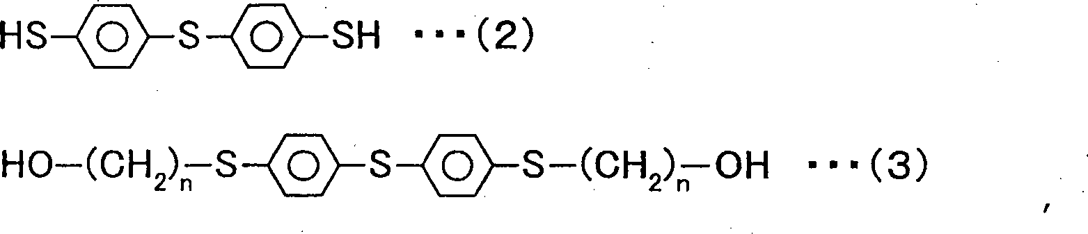
So kann das durch die allgemeine Formel 1 dargestellte Monomer leicht hergestellt werden.Thus, the monomer represented by the
Bei dem Verfahren kann der ω-Halogenalkylalkohol in der ersten Stufe 2-Halogenethanol sein und Methylacrylat kann mit der durch die allgemeine Formel 3 dargestellte Verbindung in der zweiten Stufe umgesetzt werden. Gemäß dieser Ausführungsform kann das Bis(4-mercaptophenyl)-sulfidderivat, das besonders als ein Monomer zur Bildung eines in einer elektronischen Komponente verwendeten dielektrischen Filmes bevorzugt ist, leicht hergestellt werden.In the process, the ω-haloalkyl alcohol in the first stage may be 2-haloethanol, and methyl acrylate may be reacted with the compound represented by the general formula 3 in the second stage. According to this embodiment, the bis (4-mercaptophenyl) sulfide derivative particularly preferred as a monomer for forming a dielectric film used in an electronic component can be easily produced.
Bei dem Verfahren kann die erste Stufe in Gegenwart eines Alkalimetallcarbonats durchgeführt werden, das ein basischer Katalysator ist. Des Weiteren kann die zweite Stufe in Gegenwart von Alkoxytitan oder einer Organozinnverbindung, die ein Umesterungskatalysator ist, durchgeführt werden. Gemäß dieser Ausführungsform kann das Bis(4-mercaptophenyl)sulfidderivat wirksam hergestellt werden.In the process, the first stage may be carried out in the presence of an alkali metal carbonate which is a basic catalyst. Further, the second step may be carried out in the presence of alkoxy titanium or an organotin compound which is a transesterification catalyst. According to this embodiment, the bis (4-mercaptophenyl) sulfide derivative can be efficiently produced.
Des Weiteren ist eine elektronische Komponente der vorliegenden Erfindung mit einem dielektrischen Film ausgestattet, wobei der dielektrische Film durch Ausbilden eines dünnen Filmes, welcher wenigstens eine Art von Monomer enthält, und Polymerisieren des Monomeres in dem dünnen Film, gebildet wird und das Monomer weist eine Molekülstruktur auf, in welcher Schwefel und ein aromatischer Ring kovalent gebunden sind oder eine Molekülstruktur, in welcher Schwefel und ein aromatischer Ring über eine Alkylengruppe gebunden sind. Gemäß der elektronischen Komponente der vorliegenden Erfindung kann eine elektronische Komponente mit zufrieden stellenden Eigenschaften unter hoher Feuchtigkeit und hoher Temperatur erhalten werden.Further, an electronic component of the present invention is provided with a dielectric film wherein the dielectric film is formed by forming a thin film containing at least one kind of monomer and polymerizing the monomer in the thin film, and the monomer has a molecular structure in which sulfur and an aromatic ring are covalently bonded or a molecular structure in which sulfur and an aromatic ring are bonded via an alkylene group are. According to the electronic component of the present invention, an electronic component having satisfactory properties under high humidity and high temperature can be obtained.
Die elektronische Komponente der vorliegenden Erfindung kann des Weiteren ein Paar von Elektroden umfassen, die einander gegenüber liegen, wobei wenigstens ein Teil des dielektrischen Films dazwischen angeordnet ist. Diese Ausführungsform kann eine elektronische Komponente, wie einen Kondensator, liefern, die bzw. der ausgezeichnete Eigenschaften sogar unter hoher Feuchtigkeit und hoher Temperatur aufweist.The electronic component of the present invention may further comprise a pair of electrodes facing each other with at least a part of the dielectric film interposed therebetween. This embodiment can provide an electronic component such as a capacitor, which has excellent properties even under high humidity and high temperature.
Kurze Beschreibung der Zeichnungen:Brief description of the drawings:
Nachfolgend werden Ausführungsformen der vorliegenden Erfindung unter Bezugnahme auf die begleitenden Zeichnungen beschrieben. In der nachfolgenden Beschreibung tragen gleiche Elemente gleiche Bezugsziffern, so dass eine Doppelbeschreibung vermieden werden kann.Hereinafter, embodiments of the present invention will be described with reference to the accompanying drawings. In the following description, like elements have the same reference numerals, so that a duplicate description can be avoided.
Ausführungsform 1
Bei Ausführungsform 1 werden Bis(4-mercaptophenyl)sulfidderivate beschrieben.In
Die Bis(4-mercaptophenyl)sulfidderivate der vorliegenden Erfindung sind durch die allgemeine Formel 1 unten dargestellt. 
Die Bis(4-mercaptophenyl)sulfidderivate, welche durch die allgemeine Formel 1 dargestellt sind, können durch das in Ausführungsform 2 beschriebene Verfahren hergestellt werden.The bis (4-mercaptophenyl) sulfide derivatives represented by the
Die Bis(4-mercaptophenyl)sulfidderivate, welche durch die allgemeine Formel 1 dargestellt sind, können als ein Monomer zur Ausbildung dielektrischer Filme (Harzfilme) verwendet werden, die in elektronischen Komponenten verwendet werden. Wird ein dielektrischer Film unter Verwendung dieses Monomeres gebildet, wird zunächst ein dünner Film, welcher dieses Monomer enthält, gebildet und der dünne Film wird mit Elektronenstrahlen oder Ultraviolettstrahlen bestrahlt. Wird dieses Monomer verwendet, können dielektrische Filme, die für elektronische Komponenten geeignet sind, gebildet werden. Insbesondere haben, wenn ein Monomer eines Bis(4-mercaptophenyl)sulfidderivates, bei dem R Wasserstoff und n in der allgemeinen Formel 1 gleich 2 ist, zur Bildung dielektrischer Filme für Kondensatoren verwendet werden, die Kondensatoren ausgezeichnete Eigenschaften bzw. Charakteristika sogar unter hoher Feuchtigkeit und hoher Temperatur.The bis (4-mercaptophenyl) sulfide derivatives represented by the
Gemäß einem weiteren Aspekt betrifft die vorliegende Erfindung die Verwendung einer organischen Verbindung, welche durch die allgemeine Formel 1 dargestellt ist, als Monomer eines Harzes.In another aspect, the present invention relates to the use of an organic compound represented by the
Ausführungsform 2Embodiment 2
In Ausführungsform 2 wird ein Verfahren zur Herstellung der Bis(4-mercaptophenyl)sulfidderivate, die durch die allgemeine Formel 1 dargestellt und in Ausführungsform 1 beschrieben sind, beschrieben.In Embodiment 2, a process for producing the bis (4-mercaptophenyl) sulfide derivatives represented by the
Zunächst wird eine durch die allgemeine Formel 3 unten dargestellte organische Verbindung durch Umsetzung von Bis(4-mercaptophenyl)sulfid, dargestellt durch die chemische Formel 2 unten, mit ω-Halogenalkylalkohol unter Verwendung einer Base als Katalysator bei 60°C bis 120°C während 4 bis 8 Stunden (erstes Verfahren) hergestellt. 
Das durch die chemische Formel 2 dargestellte Bis(4-mercaptophenyl)sulfid ist im Handel von Sumitomo Seika Chemicals Co., Ltd. unter dem Produktnamen MPS erhältlich.The bis (4-mercaptophenyl) sulfide represented by the chemical formula 2 is commercially available from Sumitomo Seika Chemicals Co., Ltd. available under the product name MPS.
Der in dem ersten Verfahren verwendete ω-Halogenalkylalkohol ist ein Alkohol mit einer geraden Kohlenstoffkette mit 1 bis 4 Kohlenstoffen und einer Hydroxylgruppe an einem endständigen Kohlenstoff der Kohlenstoffkette und einem Halogen am anderen endständigen Kohlenstoff der Kohlenstoffkette. Insbesondere können beispielsweise 2-Chlorethanol, 3-Chlor-1-propanol, 4-Chlor-1-butanol, 2-Bromethanol, 3-Brom-1-propanol, 2-Iodethanol und dergleichen verwendet werden. Die Anzahl der Kohlenstoffatome des ω-Halogenalkylalkohols entspricht n der Bis(4-mercaptophenyl)sulfidderivate der allgemeinen Formel 1. Beispielsweise ist, wenn 2-Chlorethanol verwendet wird, n in der allgemeinen Formel 1 gleich 2.The ω-haloalkyl alcohol used in the first process is an alcohol having a straight carbon chain of 1 to 4 carbons and a hydroxyl group on one terminal carbon of the carbon chain and a halogen on the other terminal carbon of the carbon chain. In particular, for example, 2-chloroethanol, 3-chloro-1-propanol, 4-chloro-1-butanol, 2-bromoethanol, 3-bromo-1-propanol, 2-iodoethanol and the like can be used. The number of carbon atoms of the ω-haloalkyl alcohol corresponds to n of the bis (4-mercaptophenyl) sulfide derivatives of the
Als basischer Katalysator, welcher im ersten Verfahren verwendet wird, sind Alkalimetallcarbonate, wie Na2CO3 und K2CO3, Erdalkalimetallcarbonate, wie CaCO3 und MgCO3 und Alkalimetalloxide geeignet. Unter diesen sind die Alkalimetallcarbonate bevorzugt. Als Lösungsmittel für den basischen Katalysator sind Ketone, wie Methylethylketon, Methylisobutylketon, Ether, wie Tetrahydrofuran und Dioxan, geeignet.As the basic catalyst used in the first method, alkali metal carbonates such as Na 2 CO 3 and K 2 CO 3 , alkaline earth metal carbonates such as CaCO 3 and MgCO 3, and alkali metal oxides are suitable. Among them, the alkali metal carbonates are preferable. Suitable solvents for the basic catalyst are ketones, such as methyl ethyl ketone, methyl isobutyl ketone, ethers, such as tetrahydrofuran and dioxane.
Nach dem ersten Verfahren können die Bis(4-mercaptophenyl)sulfidderivate der allgemeinen Formel 1 hergestellt werden, indem Alkylesteracrylat oder Alkylestermethacrylat und die durch die allgemeine Formel 3 dargestellte organische Verbindung in Gegenwart eines Umesterungskatalysators 6 bis 10 Stunden am Rückfluss gekocht werden (zweites Verfahren).According to the first method, the bis (4-mercaptophenyl) sulfide derivatives of
Bei dem zweiten Verfahren können Bis(4-mercaptophenyl)sulfidderivate mit R gleich Wasserstoff erhalten werden, wenn ein Alkylesteracrylat (dargestellt durch die allgemeine Formel CH2=CHCOOR', worin beispielsweise Methylgruppen, Ethylgruppen, Propylgruppen, Butylgruppen oder dergleichen für R' als eine Alkylgruppe verwendet werden), vorzugsweise Methacrylat verwendet wird. Alternativ dazu können Bis(4-mercaptophenyl)sulfidderivate mit einer Methylgruppe als R erhalten werden, wenn Alkylestermethacrylat (dargestellt durch die allgemeine Formel CH2=C(CH3)COOR'', worin beispielsweise Methylgruppen, Ethylgruppen, Propylgruppen, Butylgruppen und dergleichen für R' als eine Alkylgruppe verwendet werden können), vorzugsweise Methylmethacrylat verwendet wird.In the second method, bis (4-mercaptophenyl) sulfide derivatives having R equal to hydrogen can be obtained when an alkyl ester acrylate (represented by the general formula CH 2 = CHCOOR ', wherein, for example, methyl groups, ethyl groups, propyl groups, butyl groups or the like for R' as a Alkyl group are used), preferably methacrylate is used. Alternatively, bis (4-mercaptophenyl) sulfide derivatives having a methyl group as R may be obtained when alkyl ester methacrylate (represented by the general formula CH 2 = C (CH 3 ) COOR '' wherein, for example, methyl groups, ethyl groups, propyl groups, butyl groups and the like R 'can be used as an alkyl group), preferably methyl methacrylate is used.
Als Umesterungskatalysator, der in dem zweiten Verfahren verwendet wird, sind Alkoxytitan, wie Tetrabutyltitanat, Organozinnverbindungen, wie Dibutylzinnoxid, Dioctylzinnoxid, Dibutylzinndiacetat, Dibutylzinndilaurat, geeignet. Unter diesen wird Tetrabutyltitanat oder Dibutylzinnoxid bevorzugt. Als Menge an Alkylesteracrylat (oder Alkylestermethacrylat), die zugegeben werden muss, sind 3 bis 10 Gewichtsteile pro Gewichtsteile (Masse) organische Verbindung der allgemeinen Formel 3 bevorzugt. As the transesterification catalyst used in the second method, alkoxytitanium such as tetrabutyl titanate, organotin compounds such as dibutyltin oxide, dioctyltin oxide, dibutyltin diacetate, dibutyltin dilaurate are suitable. Among them, preferred is tetrabutyl titanate or dibutyltin oxide. As the amount of the alkyl ester acrylate (or alkyl ester methacrylate) to be added, 3 to 10 parts by weight (by weight) of the organic compound of the general formula 3 are preferable.
Bei dem oben beschriebenen Herstellungsverfahren wird bevorzugt, dass der ω-Halogenalkylalkohol im ersten Verfahren 2-Halogenethanol ist und Methylacrylat mit der durch die allgemeine Formel 3 dargestellten Verbindung im zweiten Verfahren umgesetzt wird.In the production method described above, it is preferable that the ω-haloalkyl alcohol in the first method is 2-haloethanol and methyl acrylate is reacted with the compound represented by the general formula 3 in the second method.
Das Herstellungsverfahren der Ausführungsform 2 kann die Herstellung der Bis(4-mercaptophenyl)sulfidderivate der allgemeinen Formel, die in Ausführungsform 1 beschrieben sind, erleichtern.The production method of the embodiment 2 can facilitate the preparation of the bis (4-mercaptophenyl) sulfide derivatives of the general formula described in
Ausführungsform 3Embodiment 3
In Ausführungsform 3 wird ein Beispiel eines Kondensators als eine elektronische Komponente der vorliegenden Erfindung beschrieben.
Unter Bezugnahme auf
Als Träger
Für den unteren Elektrodenfilm
Der dielektrische Film
Ein dünner Film
In dem Fall, in dem der dünne Film
In dem Fall, in dem der dünne Film
Als in dem dünnen Film 

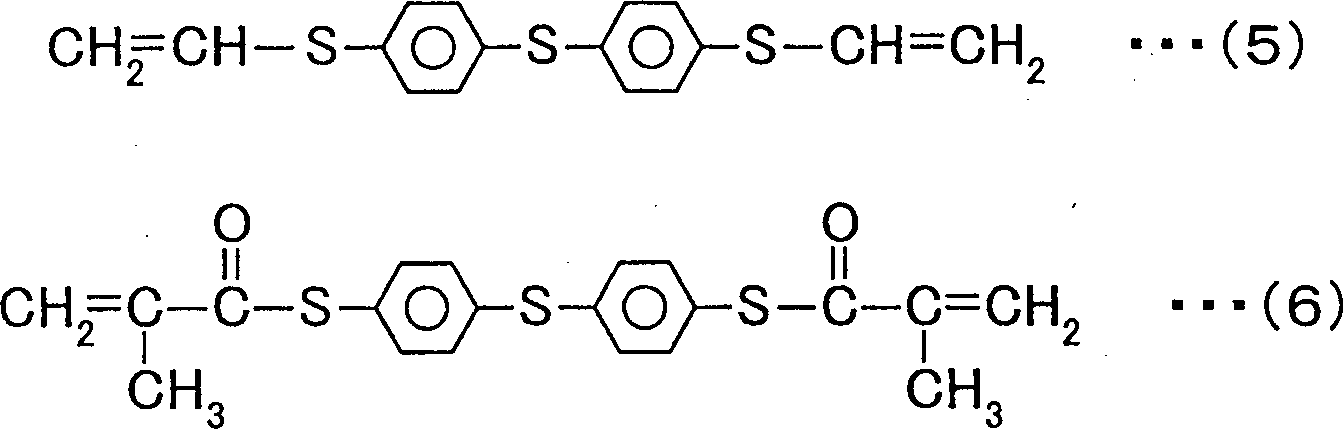
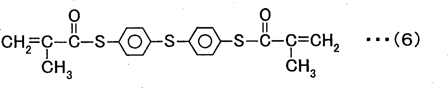
Die Monomere der allgemeinen Formel 1 können durch das in Ausführungsform 2 beschriebene Verfahren hergestellt werden. Die Monomere der allgemeinen Formel 4 können durch ein Verfahren hergestellt werden, wie es unten beschrieben wird. Die Monomere der chemischen Formeln 5 und 6 sind im Handel von Sumitomo Seika Chemicals unter den Produktnamen MPV bzw. MPSMA erhältlich.The monomers of
Für die Monomere der allgemeinen Formel 1 wird es besonders bevorzugt, dass R Wasserstoff und n gleich 2 ist. Der dünne Film
Nachfolgend wird ein Verfahren zur Herstellung der Monomere der allgemeinen Formel 4 beschrieben. Zunächst wird ein Zwischenprodukt, dargestellt durch die chemische Formel 7 unten, durch Umsetzen von p-Xyloldichlorid mit 2-Mercaptoethanol in gleicher Weise wie im ersten Verfahren zur Herstellung der Monomere der allgemeinen Formel 1 hergestellt.Hereinafter, a process for producing the monomers of the general formula 4 will be described. First, an intermediate represented by Chemical Formula 7 below is prepared by reacting p-xylene dichloride with 2-mercaptoethanol in the same manner as in the first process for producing the monomers of
![]()
![]()
Danach wird dieses Zwischenprodukt mit Methylacrylat oder Methylmethacrylat in gleicher Weise wie im zweiten Verfahren zur Herstellung des Monomers der allgemeinen Formel 1 umgesetzt und demzufolge kann das Monomer der allgemeinen Formel 4 leicht synthetisiert werden.Thereafter, this intermediate is reacted with methyl acrylate or methyl methacrylate in the same manner as in the second process for producing the monomer of the
Nachfolgend wird ein Verfahren zur Herstellung des Kondensators
Unter Bezugnahme auf
Danach wird, wie in
Dann wird in dem dünnen Film eine Polymerisationreaktion des Monomers verursacht und demzufolge wird der dielektrische Film
Danach kann, wie in
Bei dem Kondensator gemäß Ausführungsform 3 wird der dielektrische Film
Ausführungsform 4Embodiment 4
In Ausführungsform 4 wird ein weiterer Kondensator als eine elektronische Komponente der vorliegenden Erfindung beschrieben.
Bezugnehmend auf die
Der dielektrische Film
Der Kondensator
Bei dem Kondensator
BeispieleExamples
Nachfolgend wird die vorliegende Erfindung spezieller mit Hilfe von Beispielen beschrieben.Hereinafter, the present invention will be described more specifically by way of examples.
Beispiel 1example 1
In Beispiel 1 wird ein Beispiel zur Herstellung eines Monomers, das ein durch die allgemeine Formel 1 dargestelltes Bis(4-mercaptophenyl)sulfidderivat ist, wobei R Wasserstoff und n gleich 2 ist, beschrieben werden. Auch wird ein Beispiel der Herstellung eines Monomers, das ein durch die allgemeine Formel 1 dargestelltes Bis(4-mercaptophenyl)sulfidderivat ist, wobei R eine Methylgruppe und n gleich 4 ist, beschrieben.In Example 1, an example of producing a monomer which is a bis (4-mercaptophenyl) sulfide derivative represented by the
Zunächst werden 25,0 g (0,10 mol) des durch die chemische Formel 2 dargestellten Bis(4-mercaptophenyl)sulfids, 16,1 g (0,20 mol) 2-Chlorethanol, 27,6 g (0,20 mol) Kaliumcarbonat und 300 ml Methylisobutylketon in einen 1 l-Kolben gebracht und bei kontinuierlichem Rühren 6 Stunden am Rückfluss gehalten. Nach Beendigung der Reaktion wurden 50 ml einer. 5-prozentigen Salzsäurelösung nach und nach der erhaltenen Lösung unter Rühren zugegeben. Danach wurden 300 ml Toluol zugefügt. Die so erhaltene Lösung wurde wiederholt mit destilliertem Wasser gewaschen, bis der pH-Wert von 7 erreicht war. Dann wurde die gewaschene Lösung mit wasserfreiem Natriumsulfat getrocknet und das Lösungsmittel wurde durch Destillation entfernt. So wurde das durch die chemische Formel 8 unten dargestellte Zwischenprodukt in einer Menge von 32 g erhalten.First, 25.0 g (0.10 mol) of bis (4-mercaptophenyl) sulfide represented by Chemical Formula 2, 16.1 g (0.20 mol) of 2-chloroethanol, 27.6 g (0.20 mol ) Potassium carbonate and 300 ml of methyl isobutyl ketone are placed in a 1 liter flask and refluxed with continuous stirring for 6 hours. After completion of the reaction, 50 ml of a. 5% hydrochloric acid solution gradually added to the resulting solution with stirring. Thereafter, 300 ml of toluene was added. The resulting solution was washed repeatedly with distilled water until the pH of 7 was reached. Then, the washed solution was dried with anhydrous sodium sulfate, and the solvent was removed by distillation. Thus, the intermediate represented by Chemical Formula 8 below was obtained in an amount of 32 g.
![]()
![]()
Dann wurden 320 g Methylacrylat, 0,32 g Tetrabutyltitanat (1/100 Gewichtsteile bezüglich des Zwischenproduktes) und 0,16 g p-Methoxyphenol (5/1000 Gewichtsteile bezüglich des Zwischenproduktes) als Polymerisationsinhibitor zu 32 g des Zwischenproduktes, das durch die chemische Formel 8 dargestellt ist, zugegeben und dann 10 Stunden unter Rückfluss gehalten, wonach das Methylacrylat durch Destillation entfernt wurde. Das so erhaltene Reaktionsprodukt wurde in 300 ml Toluol aufgelöst und dann wurde diese Lösung nacheinander zunächst mit 20 ml 5-%iger Natriumhydroxidlösung und dann mit 50 ml 5-%iger Salzsäurelösung gewaschen. Des Weiteren wurde die Lösung mit destilliertem Wasser gewaschen, bis der pH-Wert von 7 erreicht war und dann mit wasserfreiem Natriumsulfat getrocknet. Dieser Lösung wurden 0,16 g p-Methoxyphenol zugegeben und danach wurde das Lösungsmittel durch Destillation entfernt. So wurde ein Halb-Feststoff mit einem Schmelzpunkt von 20°C erhalten. Der Halb-Feststoff wurde durch Infrarotspektroskopieanalyse und Gelpermeationschromatographie gemessen.Then, 320 g of methyl acrylate, 0.32 g of tetrabutyl titanate (1/100 part by weight relative to the intermediate) and 0.16 g of p-methoxyphenol (5/1000 parts by weight relative to the intermediate) as a polymerization inhibitor were added to 32 g of the intermediate represented by the chemical formula 8, and then refluxed for 10 hours, after which the methyl acrylate was removed by distillation. The reaction product thus obtained was dissolved in 300 ml of toluene, and then this solution was successively first with 20 ml of 5% sodium hydroxide solution and then with 50 ml of 5% hydrochloric acid solution washed. Further, the solution was washed with distilled water until the pH reached 7 and then dried with anhydrous sodium sulfate. To this solution was added 0.16 g of p-methoxyphenol, after which the solvent was removed by distillation. Thus, a semi-solid having a melting point of 20 ° C was obtained. The semi-solid was measured by infrared spectroscopic analysis and gel permeation chromatography.

Nun wird ein Beispiel der Herstellung von Bis(4-methacryloyloxybutylenthiophenyl)sulfid beschrieben werden, das ist eine durch die allgemeine Formel 1 dargestellte organische Verbindung, wobei R eine Methylgruppe und n gleich 4 ist.Now, an example of the production of bis (4-methacryloyloxybutylenthiophenyl) sulfide will be described, which is an organic compound represented by the
In diesem Falle kann das gleiche Verfahren wie das zur Herstellung des Bis(4-acryloyloxyethylenthiophenyl)sulfids, dargestellt durch die chemische Formel 9, verwendet werden, mit der Ausnahme, dass ein verschiedenes Ausgangsmaterial verwendet wird. Genauer gesagt wurde 2-Chlorethanol durch 4-Chlor-1-butanol und Methylacrylat durch Methylmethacrylat ersetzt. So wurde Bis(4-methacryloyloxybutylenthiophenyl)sulfid, dargestellt durch die chemische Formel 10, erhalten.In this case, the same method as that for producing the bis (4-acryloyloxyethylenthiophenyl) sulfide represented by the chemical formula 9 can be used, except that a different starting material is used. More specifically, 2-chloroethanol was replaced by 4-chloro-1-butanol and methyl acrylate by methyl methacrylate. Thus, bis (4-methacryloyloxybutylenthiophenyl) sulfide represented by

Beispiel 2Example 2
In Beispiel 2 wird ein Beispiel der Herstellung eines Monomers, das durch die allgemeine Formel 4 dargestellt ist, wobei R eine Methylgruppe ist, beschrieben werden.In Example 2, an example of the preparation of a monomer represented by the general formula 4 wherein R is a methyl group will be described.
Zunächst werden 17,5 g (0,10 mol) p-Xyloldichlorid, 15,6 g (0,20 mol) 2-Mercaptoethanol, 27,6 g (0,20 mol) Kaliumcarbonat und 300 ml Methylisobutylketon in einem 1 l-Kolben vorgelegt und unter kontinuierlichem Rühren unter Rückfluss 6 Stunden umgesetzt. Nach Beendigung der Umsetzung wurde die erhaltene Lösung in gleicher Weise wie in Beispiel 1 behandelt und demgemäß wurde das Zwischenprodukt, dargestellt durch die chemische Formel 7 unten, in einer Menge von 23 g erhalten.First, 17.5 g (0.10 mol) of p-xylene dichloride, 15.6 g (0.20 mol) of 2-mercaptoethanol, 27.6 g (0.20 mol) of potassium carbonate and 300 ml of methyl isobutyl ketone in a 1 l Put the flask and reacted with continuous stirring under reflux for 6 hours. After completion of the reaction, the resulting solution was treated in the same manner as in Example 1, and accordingly, the intermediate represented by Chemical Formula 7 below was obtained in an amount of 23 g.
![]()
![]()
Dann wurden 230 g Methylacrylat, 0,23 g Tetrabutyltitanat (1/100 Gewichtsteile bezüglich des Zwischenproduktes) und 0,12 g p-Methoxyphenol (5/1000 Gewichtsteile bezüglich des Zwischenproduktes) als Polymerisationsinhibitor zu 23 g des Zwischenproduktes, das durch die chemische Formel 7 dargestellt ist, zugegeben und dann 10 Stunden unter Rückfluss gehalten und Methylacrylat wurde durch Destillation entfernt. Das so erhaltene Reaktionsprodukt wurde in gleicher Weise wie in Beispiel 1 behandelt und so wurde eine transparente hellgelbe Flüssigkeit erhalten. Diese Flüssigkeit wurde durch Infrarotspektroskopieanalyse und GPC vermessen.Then, 230 g of methyl acrylate, 0.23 g of tetrabutyl titanate (1/100 part by weight with respect to the intermediate) and 0.12 g of p-methoxyphenol (5/1000 parts by weight relative to the intermediate) as a polymerization inhibitor were added to 23 g of the intermediate represented by the chemical formula 7 and then refluxed for 10 hours, and methyl acrylate was removed by distillation. The reaction product thus obtained was treated in the same manner as in Example 1 to obtain a transparent pale yellow liquid. This liquid was measured by infrared spectroscopic analysis and GPC.

Das Monomer der allgemeinen Formel 1 mit R gleich Wasserstoff kann durch das gleiche Verfahren, das oben beschrieben ist, hergestellt werden, mit der Ausnahme, dass Methylacrylat anstelle von Methylmethacrylat mit dem durch die chemische Formel 7 dargestellten Zwischenprodukt umgesetzt wird.The monomer of
Beispiel 3Example 3
In Beispiel 3 wird ein Beispiel der Herstellung des in
Zunächst wurde ein PET-Substrat
Danach wurde der dünne Film
Danach wurde der dünne Film mit beschleunigten Elektronen bei –15 kV bei einer Dichte von 50 μA/cm2 2 Sekunden lang bestrahlt, um das Monomer in dem dünnen Film zu polymerisieren und so wurde der dielektrische Film
Danach wurde der obere Elektrodenfilm
In Beispiel 3 wurden fünf verschiedene Kondensatoren hergestellt, indem das Monomer der chemischen Formel 9, das Monomer der chemischen Formel 4, das Monomer der chemischen Formel 11, enthaltend 3 Gew.-% IRGANOX 1520L als Antioxidationsmittel, das Monomer der chemischen Formel 5 und das Monomer der chemischen Formel 6 verwendet wurden. Demzufolge wurden Arbeitsproben 1 bis 5 erhalten.In Example 3, five different capacitors were prepared by using the monomer of Chemical Formula 9, the monomer of Chemical Formula 4, the monomer of
Des Weiteren wurden als Vergleichsbeispiele zwei Typen von Kondensatoren (Vergleichsbeispiele 1 und 2) hergestellt, unter Verwendung von Monomeren, die durch die chemischen Formeln A und B dargestellt sind.Further, as comparative examples, two types of capacitors (Comparative Examples 1 and 2) were prepared by using monomers represented by the chemical formulas A and B.

Hinsichtlich der oben beschriebenen sieben Typen von Kondensatoren wurde (i) eine Feuchtigkeitsabsorption-Kapazitätänderungsverhältnis und (ii) ein Hochtemperaturbelastung-Kapazitätänderungsverhältnis gemessen. Für die Kondensatoren, welche mit den Monomeren der chemischen Formeln 9, A und B hergestellt worden waren, wurden die Änderungen in der Dicke beim Eintauchen der Kondensatoren in heißes Wasser untersucht. Das Bewertungsverfahren wird später beschrieben werden. Tabelle 1 zeigt die Bewertungsergebnisse. Tabelle 1
Wie aus Tabelle 1 gesehen werden kann, zeigen die Kondensatoren der Arbeitsproben 1 bis 5 bessere Charakteristika als jene der Kondensatoren der Vergleichsproben 1 und 2 bei Bewertung sowohl des Feuchtigkeitsabsorption-Kapazitätänderungsverhältnisses als auch des Hochtemperaturbelastung-Kapazitätänderungsverhältnisses. Genauer gesagt wurden Kondensatoren mit ausgezeichneten Charakteristika sogar bei hoher Feuchtigkeit und hoher Temperatur durch Ausbilden dielektrischer Filme der Kondensatoren mit Monomeren erhalten, welche eine Molekülstruktur, in der Schwefel und ein aromatischer Ring kovalent gebunden sind oder eine Molekülstruktur, in der Schwefel und ein aromatischer Ring über eine Alkylengruppe verbunden sind, aufweisen.As can be seen from Table 1, the capacitors of
Nachfolgend wird das Bewertungsverfahren der in Tabelle 1 gezeigten Charakteristika genauer beschrieben werden.
- (i) Das Feuchtigkeitsabsorptionskapazität-Änderungsverhältnis wurde auf folgende Weise bewertet. Zunächst wurde ein Kondensator in einer 105°
C Atmosphäre 10 Stunden getrocknet und die Anfangskapazität C11 wurde gemessen. Die Kapazität wurde gemessen, während eine Sinuswelle mit einerFrequenz von 1 kHz und eineSpannung von 1 Vrms auf den Kondensator angelegt wurde. Danach wurde der Kondensator in einer Atmosphäre bei einer Temperatur von 60°C und einer relativen Feuchtigkeit von 95% 100 Stunden gelagert. Dann wurde die Kapazität C12 nach der Lagerung (die Kapazität, wenn der Kondensator Feuchtigkeit absorbierte) und den gleichen Bedingungen wie für die Anfangskapazität gemessen. Das Feuchtigkeitsabsorption-Kapazitätänderungsverhältnis ist ein Wert, der durch (C12 – C11)/C11 × 100(%) dargestellt ist. Je kleiner das Feuchtigkeitsabsorption-Kapazitätänderungsverhältnis ist, desto höher ist die Kapazitätsstabilität in einer feuchten Atmosphäre und solche Kondensatoren mit einem kleinen Änderungsverhältnis werden als Produkt bevorzugt. Daher ist es besonders wichtig, dass das Feuchtigkeitsabsorption-Kapazitätänderungsverhältnis so klein wie möglich ist. - (ii) Das Hochtemperaturbelastung-Kapazitätänderungsverhältnis wurde auf folgende Weise bewertet. Zunächst wurde ein Kondensator in einer 105°
C Atmosphäre 10 Stunden getrocknet und die Anfangskapazität C21 wurde gemessen. Die Kapazität wurde gemessen, während eine Sinuswelle mit einerFrequenz 1 kHz und eineSpannung von 1 Vrms an den Kondensator angelegt wurden. Danach wurde der Kondensator 50.000 Stunden in einer Atmosphäre bei einer Temperatur von 105°C gelagert, während eine Spannung von 16 V angewendet wurde. Dann wurde die Kapazität C22 nach der Lagerung unter den gleichen Bedingungen wie für die Anfangskapazität gemessen. Das Hochtemperaturbelastung-Kapazitätänderungsverhältnis ist ein Wert, der durch (C22 – C21)/C21 × 100(%) dargestellt ist. Ein Kondensator mit einem kleinen absoluten Wert des Hochtemperaturbelastung-Kapazitätänderungsverhältnisses wird weniger wahrscheinlich bei hohen Temperaturen oxidiert und ein solcher Kondensator ist ein bevorzugtes Produkt. Insbesondere wurde in den vergangenen Jahren die Hochtemperaturresistenz elektronischer Komponenten wichtig, da CPUs bei hoher Geschwindigkeit betrieben werden. Daher ist die Niedrigkeit des absoluten Wertes des Hochtemperaturbelastung-Kapazitätänderungsverhältnisses eine wichtige Anzeige bei der Bewertung von Kondensatoren. - (iii) Die Änderung der Dicke beim Eintauchen der Kondensatoren in heißes Wasser wurde auf folgende Weise gemessen. Zunächst wurde die Dicke eines Kondensators gemessen. Dann wurde der Kondensator in heißes Wasser von 90°C für 3,5 Stunden eingetaucht. Danach wurde der Kondensator aus dem heißen Wasser herausgenommen und die Dicke wurde erneut gemessen. Danach wurden die Dicken vor und nach dem Eintauchen in heißes Wasser verglichen. Je größer die Änderung der Dicke ist, desto mehr Feuchtigkeit absorbiert der dielektrische Film und die Haftung bzw. Adhäsion zwischen dem dielektrischen Film und dem Elektrodenfilm aus Metall wird herabgesetzt. Daher weist ein Kondensator mit einer geringen Änderung der Dicke eine höhere Haftung zwischen dem dielektrischen Film und dem Elektrodenfilm auf, so dass ein solcher Kondensator ein bevorzugtes Produkt ist.
- (i) The moisture absorption capacity change ratio was evaluated in the following manner. First, a capacitor was dried in a 105 ° C atmosphere for 10 hours, and the initial capacity C 11 was measured. The capacitance was measured while applying a sine wave at a frequency of 1 kHz and a voltage of 1 Vrms to the capacitor. Thereafter, the condenser was stored in an atmosphere at a temperature of 60 ° C and a relative humidity of 95% for 100 hours. Then, the capacity C 12 after storage (the capacity when the capacitor absorbed moisture) and the same conditions as for the initial capacity was measured. The moisture absorption capacity change ratio is a value represented by (C 12 -C 11 ) / C 11 × 100 (%). The smaller the moisture absorption-capacity change ratio, the higher the capacity stability in a humid atmosphere, and those having a small change ratio are preferable as a product. Therefore, it is especially important that the moisture absorption capacity change ratio is as small as possible.
- (ii) The high-temperature load-capacity change ratio was evaluated in the following manner. First, a capacitor was dried in a 105 ° C atmosphere for 10 hours, and the initial capacity C 21 was measured. The capacitance was measured while applying a sine wave with a frequency of 1 kHz and a voltage of 1 Vrms to the capacitor. Thereafter, the capacitor was stored for 50,000 hours in an atmosphere at a temperature of 105 ° C while applying a voltage of 16V. Then, the capacity C 22 after storage was measured under the same conditions as for the initial capacity. The high-temperature load capacity change ratio is a value represented by (C 22 -C 21 ) / C 21 × 100 (%). A capacitor having a small absolute value of the high temperature load-capacity change ratio is less likely to be oxidized at high temperatures and such a capacitor is a preferred product. In particular, the high-temperature resistance of electronic components has become important in recent years because CPUs are operated at high speed. Therefore, the low of the absolute value of the high-temperature load-capacity change ratio is an important indication in the evaluation of capacitors.
- (iii) The change in the thickness when immersing the capacitors in hot water was measured in the following manner. First, the thickness of a capacitor was measured. Then, the condenser was immersed in hot water of 90 ° C for 3.5 hours. Thereafter, the condenser was taken out of the hot water and the thickness was measured again. Thereafter, the thicknesses before and after immersion in hot water were compared. The larger the change in the thickness, the more moisture the dielectric film absorbs, and the adhesion between the dielectric film and the metal electrode film is lowered. Therefore, a capacitor having a small change in thickness has a higher adhesion between the dielectric film and the electrode film, so that such a capacitor is a preferable product.
Des Weiteren wurde der (dielektrische) Verlusttangens (tanδ) hinsichtlich jeder Probe bewertet und die Ergebnisse waren so, dass die Kondensatoren der Arbeitsproben 1 bis 5 Charakteristika zeigten, die gleich jenen der Vergleichsproben 1 und 2 sind, oder sogar bessere Charakteristika. Der (dielektrische) Verlusttangens (tanδ) wurde gemessen, während eine Sinuswelle mit einer Frequenz von 1 kHz und eine Spannung von 1 Vrms auf den Kondensator angewendet wurde. Je kleiner der (dielektrische) Verlusttangens ist, desto kleiner ist die durch den Kondensator selbst verbrauchte Energie, so dass ein solcher Kondensator mit einem kleinen (dielektrischen) Verlusttangens ein bevorzugtes Produkt ist.Further, the (dielectric) loss tangent (tanδ) was evaluated with respect to each sample, and the results were such that the capacitors of
Bei den oben beschriebenen Ausführungsformen und Beispielen wurde der Fall beschrieben, in dem die elektronische Komponente der vorliegenden Erfindung ein Kondensator ist. Jedoch ist die elektronische Komponente der vorliegenden Erfindung nicht darauf beschränkt und jede elektronische Komponente kann verwendet werden, solange der in den obigen Ausführungsformen beschriebene dielektrische Film vorgesehen ist. Genauer gesagt kann die vorliegende Erfindung beispielsweise für Spulen, Resistoren, kapazitive Zellen, Trägerelemente anderer elektronischer Komponenten oder dergleichen verwendet werden.In the above-described embodiments and examples, the case where the electronic component of the present invention is a capacitor has been described. However, the electronic component of the present invention is not limited thereto, and any electronic component may be used as long as the dielectric film described in the above embodiments is provided. More specifically, the present invention can be used, for example, for coils, resistors, capacitive cells, support members of other electronic components, or the like.
Die Ausführungsformen der vorliegenden Erfindung wurden oben im Wege von Beispielen beschrieben. Jedoch ist die vorliegenden Erfindung nicht auf die oben beschriebenen Ausführungsformen beschränkt und kann auf weitere Ausführungsformen, die auf dem technischen Gedanken der vorliegenden Erfindung basieren, angewendet werden.The embodiments of the present invention have been described above by way of examples. However, the present invention is not limited to the above-described embodiments, and may be applied to other embodiments based on the technical idea of the present invention.
Gewerbliche AnwendbarkeitIndustrial Applicability
Wie oben beschrieben worden ist, liefert die vorliegende Erfindung elektronische Komponenten, umfassend einen dielektrischen Film, enthaltend Bis(4-mercaptophenyl)sulfidderivate, dargestellt durch die allgemeine Formel 1. Die Bis(4-mercaptophenyl)sulfidderivate, dargestellt durch die allgemeine Formel 1, sind für elektronische Komponenten, wie Kondensatoren, Spulen, Resistoren, kapazitive Zellen, Trägerelemente anderer elektronischer Komponenten oder dergleichen nützlich. Wird ein dielektrischer Film unter Verwendung der Bis(4-mercaptophenyl)sulfidderivate gebildet und in einer elektronischen Komponente verwendet, kann die elektronische Komponente ausgezeichnete Charakteristika, sogar bei hoher Feuchtigkeit und hoher Temperatur, aufweisen.As described above, the present invention provides electronic components comprising a dielectric film containing bis (4-mercaptophenyl) sulfide derivatives represented by the
Das angegebene Verfahren zur Herstellung von Bis(4-mercaptophenyl)sulfidderivaten macht es möglich, die Bis(4-mercaptophenyl)sulfidderivate, dargestellt durch die allgemeine Formel 1, leicht herzustellen.The specified method for producing bis (4-mercaptophenyl) sulfide derivatives makes it possible to easily prepare the bis (4-mercaptophenyl) sulfide derivatives represented by the
Darüber hinaus kann gemäß der elektronischen Komponente der vorliegenden Erfindung eine elektronische Komponente mit ausgezeichneten Eigenschaften, sogar bei hoher Feuchtigkeit und hoher Temperatur, erhalten werden. Insbesondere kann ein hochqualitativer Kondensator mit reduzierten Änderungen der Charakteristika infolge der Umwelt, durch Anwenden der vorliegenden Erfindung für den Kondensator erhalten werden.Moreover, according to the electronic component of the present invention, an electronic component having excellent properties even at high humidity and high temperature can be obtained. In particular, a high quality capacitor with reduced changes in characteristics due to the environment can be obtained by applying the present invention to the capacitor.
Claims (4)


Applications Claiming Priority (5)
| Application Number | Priority Date | Filing Date | Title |
|---|---|---|---|
| JP2000-222712 | 2000-07-24 | ||
| JP2000-222713 | 2000-07-24 | ||
| JP2000222713A JP3441425B2 (en) | 2000-07-24 | 2000-07-24 | Capacitor |
| JP2000222712A JP2002037770A (en) | 2000-07-24 | 2000-07-24 | Bis(4-mercaptophenyl)sulfide derivative and method for producing the same |
| PCT/JP2001/006315 WO2002008180A1 (en) | 2000-07-24 | 2001-07-23 | Bis(4-mercaptophenyl) sulfide derivatives, process for the preparation thereof and electronic components |
Publications (2)
| Publication Number | Publication Date |
|---|---|
| DE10196442T1 DE10196442T1 (en) | 2003-07-10 |
| DE10196442B4 true DE10196442B4 (en) | 2011-03-31 |
Family
ID=26596572
Family Applications (1)
| Application Number | Title | Priority Date | Filing Date |
|---|---|---|---|
| DE10196442T Expired - Fee Related DE10196442B4 (en) | 2000-07-24 | 2001-07-23 | Electronic component comprising a dielectric film of at least one bis (4-mercaptophenyl) sulfide derivative |
Country Status (8)
| Country | Link |
|---|---|
| US (1) | US7006344B2 (en) |
| KR (1) | KR100556214B1 (en) |
| CN (1) | CN1214005C (en) |
| DE (1) | DE10196442B4 (en) |
| GB (1) | GB2388840B (en) |
| MY (1) | MY141740A (en) |
| TW (1) | TWI245034B (en) |
| WO (1) | WO2002008180A1 (en) |
Families Citing this family (10)
| Publication number | Priority date | Publication date | Assignee | Title |
|---|---|---|---|---|
| WO2008101806A2 (en) * | 2007-02-20 | 2008-08-28 | Basf Se | High refractive index monomers, compositions and uses thereof |
| CN102385985A (en) * | 2011-08-05 | 2012-03-21 | 贵州大学 | Metal thin film capacitor and preparation method thereof |
| SG11201507619PA (en) | 2013-03-15 | 2015-10-29 | Ct For Drug Res And Dev | Cytotoxic and anti-mitotic compounds, and methods of using the same |
| CN106255513B (en) | 2013-12-27 | 2022-01-14 | 酵活有限公司 | Sulfonamide-containing linking systems for drug conjugates |
| CA2960899C (en) | 2014-09-17 | 2021-08-17 | Zymeworks Inc. | Cytotoxic and anti-mitotic compounds, and methods of using the same |
| JP6005313B1 (en) * | 2016-02-10 | 2016-10-12 | 古河電気工業株式会社 | Conductive adhesive film and dicing die bonding film using the same |
| JP6005312B1 (en) | 2016-02-10 | 2016-10-12 | 古河電気工業株式会社 | Conductive adhesive film and dicing die bonding film using the same |
| JP5989928B1 (en) | 2016-02-10 | 2016-09-07 | 古河電気工業株式会社 | Conductive adhesive film and dicing die bonding film using the same |
| JP5972489B1 (en) | 2016-02-10 | 2016-08-17 | 古河電気工業株式会社 | Conductive adhesive film and dicing die bonding film using the same |
| JP5972490B1 (en) | 2016-02-10 | 2016-08-17 | 古河電気工業株式会社 | Conductive adhesive composition, and conductive adhesive film and dicing / die bonding film using the same |
Citations (6)
| Publication number | Priority date | Publication date | Assignee | Title |
|---|---|---|---|---|
| US2636022A (en) * | 1950-09-14 | 1953-04-21 | Sprague Electric Co | Dielectric compositions |
| US5125138A (en) * | 1983-12-19 | 1992-06-30 | Spectrum Control, Inc. | Miniaturized monolithic multi-layer capacitor and apparatus and method for making same |
| DE69103246T2 (en) * | 1990-10-24 | 1995-01-12 | Mitsubishi Petrochemical Co | Resin for highly refractive lenses. |
| JPH08183816A (en) * | 1994-11-01 | 1996-07-16 | Sumitomo Seika Chem Co Ltd | Curable resin composition |
| JPH1039111A (en) * | 1996-07-22 | 1998-02-13 | Nippon Sheet Glass Co Ltd | Planer microlens |
| EP0795765B1 (en) * | 1996-03-13 | 2002-09-25 | Tokuyama Corporation | Photopolymerizable composition and transparent cured product thereof |
Family Cites Families (26)
| Publication number | Priority date | Publication date | Assignee | Title |
|---|---|---|---|---|
| US4046744A (en) * | 1976-07-28 | 1977-09-06 | Rohm And Haas Company | Thermosetting coatings based on ketoxime-blocked isocyanates and oxazolidines |
| JPS57187327A (en) | 1981-05-13 | 1982-11-18 | Toray Ind Inc | Poly-p-phenylene sulfide film |
| EP0147696B1 (en) | 1983-12-19 | 1991-07-10 | SPECTRUM CONTROL, INC. (a Pennsylvania corporation) | Miniaturized monolithic multi-layer capacitor and apparatus and method for making |
| JPS61272917A (en) * | 1985-05-29 | 1986-12-03 | 東レ株式会社 | Capacitor |
| JPS6331929A (en) | 1986-07-25 | 1988-02-10 | Toshiba Corp | Intermittent feeder for parts |
| US5013823A (en) * | 1988-12-02 | 1991-05-07 | Kureha Kagaku Kogyo K.K. | Poly(arylene sulfide) sheet and production process thereof |
| JPH02247212A (en) | 1989-03-20 | 1990-10-03 | Showa Denko Kk | Curable composition |
| JPH02258819A (en) | 1989-03-31 | 1990-10-19 | Showa Denko Kk | New polymerizable monomer |
| JPH06151652A (en) | 1992-11-16 | 1994-05-31 | Nitto Denko Corp | Semiconductor device |
| JPH06291346A (en) | 1993-04-02 | 1994-10-18 | Toray Ind Inc | Photoelectromotive force device |
| US5859145A (en) * | 1993-07-13 | 1999-01-12 | Chevron Chemical Company | Compositions having ethylenic backbone and benzylic, allylic, or ether-containing side-chains, oxygen scavenging compositions containing same, and process for making these compositions by esterification or transesterification of a polymer melt |
| EP0952466A3 (en) * | 1994-10-18 | 2000-05-03 | Mitsubishi Rayon Co., Ltd. | Lens sheet |
| JPH08157320A (en) | 1994-12-06 | 1996-06-18 | Mitsui Toatsu Chem Inc | Dental material and dental resin composition |
| JP3509468B2 (en) | 1996-05-31 | 2004-03-22 | 三菱化学株式会社 | Transparent conductive sheet |
| JP3482815B2 (en) | 1996-05-31 | 2004-01-06 | 三菱化学株式会社 | Transparent conductive sheet |
| JPH10151676A (en) | 1996-11-25 | 1998-06-09 | Mitsubishi Chem Corp | Cutting of photo-set crosslinked resin sheet |
| JP3391677B2 (en) | 1997-11-18 | 2003-03-31 | 松下電器産業株式会社 | Laminates and capacitors |
| JPH11322897A (en) | 1998-05-20 | 1999-11-26 | Nippon Kayaku Co Ltd | Photocationically polymerizable epoxy resin-based solid composition and article |
| JP2000218738A (en) | 1999-02-01 | 2000-08-08 | Toray Ind Inc | Biaxially oriented polyphenylene sulfide laminated film and capacitor using the same |
| JP3785012B2 (en) | 1999-03-24 | 2006-06-14 | 富士通株式会社 | Photosensitive high dielectric composition, photosensitive high dielectric film pattern forming method comprising the composition, and capacitor built-in multilayer circuit board manufactured using the composition |
| JP2001064364A (en) | 1999-08-26 | 2001-03-13 | Hitachi Chem Co Ltd | Epoxy resin molding material for sealing and electronic part device |
| JP2001064363A (en) | 1999-08-26 | 2001-03-13 | Hitachi Chem Co Ltd | Epoxy resin molding material for sealing and electronic part device |
| JP2001310911A (en) * | 2000-04-28 | 2001-11-06 | Sumitomo Seika Chem Co Ltd | Dielectric substance forming material and dielectric film |
| JP2002020508A (en) | 2000-07-04 | 2002-01-23 | Toray Ind Inc | Polyphenylene sulfide film and capacitor |
| JP2002037770A (en) | 2000-07-24 | 2002-02-06 | Matsushita Electric Ind Co Ltd | Bis(4-mercaptophenyl)sulfide derivative and method for producing the same |
| US6541591B2 (en) * | 2000-12-21 | 2003-04-01 | 3M Innovative Properties Company | High refractive index microreplication resin from naphthyloxyalkylmethacrylates or naphthyloxyacrylates polymers |
-
2001
- 2001-07-20 TW TW090117780A patent/TWI245034B/en not_active IP Right Cessation
- 2001-07-23 US US10/332,548 patent/US7006344B2/en not_active Expired - Lifetime
- 2001-07-23 CN CNB018159621A patent/CN1214005C/en not_active Expired - Fee Related
- 2001-07-23 GB GB0303935A patent/GB2388840B/en not_active Expired - Fee Related
- 2001-07-23 KR KR1020037001024A patent/KR100556214B1/en not_active IP Right Cessation
- 2001-07-23 DE DE10196442T patent/DE10196442B4/en not_active Expired - Fee Related
- 2001-07-23 WO PCT/JP2001/006315 patent/WO2002008180A1/en active IP Right Grant
- 2001-07-24 MY MYPI20013497A patent/MY141740A/en unknown
Patent Citations (6)
| Publication number | Priority date | Publication date | Assignee | Title |
|---|---|---|---|---|
| US2636022A (en) * | 1950-09-14 | 1953-04-21 | Sprague Electric Co | Dielectric compositions |
| US5125138A (en) * | 1983-12-19 | 1992-06-30 | Spectrum Control, Inc. | Miniaturized monolithic multi-layer capacitor and apparatus and method for making same |
| DE69103246T2 (en) * | 1990-10-24 | 1995-01-12 | Mitsubishi Petrochemical Co | Resin for highly refractive lenses. |
| JPH08183816A (en) * | 1994-11-01 | 1996-07-16 | Sumitomo Seika Chem Co Ltd | Curable resin composition |
| EP0795765B1 (en) * | 1996-03-13 | 2002-09-25 | Tokuyama Corporation | Photopolymerizable composition and transparent cured product thereof |
| JPH1039111A (en) * | 1996-07-22 | 1998-02-13 | Nippon Sheet Glass Co Ltd | Planer microlens |
Non-Patent Citations (4)
| Title |
|---|
| (PAJ) JP 08183816 A |
| HCAPLUS-Abstract & JP 10039111 A * |
| JP 10039111 (HCAPLUS-Abstract) |
| PAJ & JP 08183816 A * |
Also Published As
| Publication number | Publication date |
|---|---|
| DE10196442T1 (en) | 2003-07-10 |
| GB2388840B (en) | 2004-09-08 |
| KR20030029634A (en) | 2003-04-14 |
| TWI245034B (en) | 2005-12-11 |
| CN1461296A (en) | 2003-12-10 |
| US7006344B2 (en) | 2006-02-28 |
| CN1214005C (en) | 2005-08-10 |
| US20030189808A1 (en) | 2003-10-09 |
| KR100556214B1 (en) | 2006-03-03 |
| GB0303935D0 (en) | 2003-03-26 |
| WO2002008180A1 (en) | 2002-01-31 |
| GB2388840A (en) | 2003-11-26 |
| MY141740A (en) | 2010-06-15 |
Similar Documents
| Publication | Publication Date | Title |
|---|---|---|
| DE3027574C2 (en) | Process for coating various surfaces and suitable means | |
| EP0065285B1 (en) | Photopolymerisable composition and copying material made therefrom | |
| EP0054700B1 (en) | Composition polymwrisable by irradiation, and radiation sensible recording material produced therefrom | |
| EP0031305B1 (en) | Compositions containing acrylate and their polymerisation | |
| DE10196442B4 (en) | Electronic component comprising a dielectric film of at least one bis (4-mercaptophenyl) sulfide derivative | |
| DE3621474C1 (en) | Process for forming a film structure of a fluorinated, aliphatic compound on a solid support surface | |
| DE10229218A1 (en) | Alkylenedioxythiophene dimers and trimers | |
| DE2917151C2 (en) | Electrostatographic or electrophotographic recording material | |
| CH639294A5 (en) | METHOD FOR PRODUCING A CLEAR CONDUCTIVE LAYER ON A SUBSTRATE. | |
| DE2635929A1 (en) | PHOTOPOLYMERIZABLE EPOXY RESINS | |
| EP0760372B9 (en) | Water containing solutions of acryl-functional organosilanes | |
| DE2519401C3 (en) | Coating compound polymerizable by current radiation | |
| EP0069069B1 (en) | Polymerisable compositions and polymerisation products resulting therefrom | |
| DE3106570C2 (en) | Acryloyloxy- or methacryloyloxy-terminated polyesters | |
| EP1338617A2 (en) | Transparant layers of Polythiophene having high conductivity | |
| DE2044233B2 (en) | Photopolymerizable compounds | |
| EP0554798A2 (en) | Coating for plastic foils | |
| EP1352918B1 (en) | Alkylenedioxythiophenes and poly(alkylenedioxythiophene)s with side groups containing urethane groups | |
| EP0281808A2 (en) | Radiation cross-linkable polymer system for application as photoresist and dielectric for micro wiring | |
| DE2407301C3 (en) | Curable coating composition and method for its preparation | |
| DE2450381C3 (en) | Radiation-sensitive material and its use | |
| DE3114647A1 (en) | RADIATION-HARDENABLE PREPARATION | |
| DE1106181B (en) | Process for producing a copying layer for planographic printing plates from epoxy resins | |
| AT511707B1 (en) | PHOTO PAINT | |
| CH645395A5 (en) | Composite coating materials |
Legal Events
| Date | Code | Title | Description |
|---|---|---|---|
| 8110 | Request for examination paragraph 44 | ||
| 8127 | New person/name/address of the applicant |
Owner name: PANASONIC CORP., KADOMA, OSAKA, JP |
|
| R020 | Patent grant now final | ||
| R020 | Patent grant now final |
Effective date: 20110817 |
|
| R119 | Application deemed withdrawn, or ip right lapsed, due to non-payment of renewal fee | ||
| R119 | Application deemed withdrawn, or ip right lapsed, due to non-payment of renewal fee |
Effective date: 20150203 |