CN102316680A - The method of wiring substrate and manufacturing wiring substrate - Google Patents
The method of wiring substrate and manufacturing wiring substrate Download PDFInfo
- Publication number
- CN102316680A CN102316680A CN2011101979171A CN201110197917A CN102316680A CN 102316680 A CN102316680 A CN 102316680A CN 2011101979171 A CN2011101979171 A CN 2011101979171A CN 201110197917 A CN201110197917 A CN 201110197917A CN 102316680 A CN102316680 A CN 102316680A
- Authority
- CN
- China
- Prior art keywords
- electrode pad
- insulating barrier
- adjustment layer
- periphery
- wiring substrate
- Prior art date
- Legal status (The legal status is an assumption and is not a legal conclusion. Google has not performed a legal analysis and makes no representation as to the accuracy of the status listed.)
- Pending
Links
Images


Classifications
-
- H—ELECTRICITY
- H05—ELECTRIC TECHNIQUES NOT OTHERWISE PROVIDED FOR
- H05K—PRINTED CIRCUITS; CASINGS OR CONSTRUCTIONAL DETAILS OF ELECTRIC APPARATUS; MANUFACTURE OF ASSEMBLAGES OF ELECTRICAL COMPONENTS
- H05K3/00—Apparatus or processes for manufacturing printed circuits
- H05K3/10—Apparatus or processes for manufacturing printed circuits in which conductive material is applied to the insulating support in such a manner as to form the desired conductive pattern
- H05K3/20—Apparatus or processes for manufacturing printed circuits in which conductive material is applied to the insulating support in such a manner as to form the desired conductive pattern by affixing prefabricated conductor pattern
- H05K3/205—Apparatus or processes for manufacturing printed circuits in which conductive material is applied to the insulating support in such a manner as to form the desired conductive pattern by affixing prefabricated conductor pattern using a pattern electroplated or electroformed on a metallic carrier
-
- H—ELECTRICITY
- H05—ELECTRIC TECHNIQUES NOT OTHERWISE PROVIDED FOR
- H05K—PRINTED CIRCUITS; CASINGS OR CONSTRUCTIONAL DETAILS OF ELECTRIC APPARATUS; MANUFACTURE OF ASSEMBLAGES OF ELECTRICAL COMPONENTS
- H05K3/00—Apparatus or processes for manufacturing printed circuits
- H05K3/40—Forming printed elements for providing electric connections to or between printed circuits
-
- H—ELECTRICITY
- H01—ELECTRIC ELEMENTS
- H01L—SEMICONDUCTOR DEVICES NOT COVERED BY CLASS H10
- H01L21/00—Processes or apparatus adapted for the manufacture or treatment of semiconductor or solid state devices or of parts thereof
- H01L21/02—Manufacture or treatment of semiconductor devices or of parts thereof
- H01L21/04—Manufacture or treatment of semiconductor devices or of parts thereof the devices having at least one potential-jump barrier or surface barrier, e.g. PN junction, depletion layer or carrier concentration layer
- H01L21/48—Manufacture or treatment of parts, e.g. containers, prior to assembly of the devices, using processes not provided for in a single one of the subgroups H01L21/06 - H01L21/326
- H01L21/4814—Conductive parts
- H01L21/4846—Leads on or in insulating or insulated substrates, e.g. metallisation
- H01L21/4857—Multilayer substrates
-
- H—ELECTRICITY
- H01—ELECTRIC ELEMENTS
- H01L—SEMICONDUCTOR DEVICES NOT COVERED BY CLASS H10
- H01L21/00—Processes or apparatus adapted for the manufacture or treatment of semiconductor or solid state devices or of parts thereof
- H01L21/67—Apparatus specially adapted for handling semiconductor or electric solid state devices during manufacture or treatment thereof; Apparatus specially adapted for handling wafers during manufacture or treatment of semiconductor or electric solid state devices or components ; Apparatus not specifically provided for elsewhere
- H01L21/683—Apparatus specially adapted for handling semiconductor or electric solid state devices during manufacture or treatment thereof; Apparatus specially adapted for handling wafers during manufacture or treatment of semiconductor or electric solid state devices or components ; Apparatus not specifically provided for elsewhere for supporting or gripping
- H01L21/6835—Apparatus specially adapted for handling semiconductor or electric solid state devices during manufacture or treatment thereof; Apparatus specially adapted for handling wafers during manufacture or treatment of semiconductor or electric solid state devices or components ; Apparatus not specifically provided for elsewhere for supporting or gripping using temporarily an auxiliary support
-
- H—ELECTRICITY
- H01—ELECTRIC ELEMENTS
- H01L—SEMICONDUCTOR DEVICES NOT COVERED BY CLASS H10
- H01L23/00—Details of semiconductor or other solid state devices
- H01L23/12—Mountings, e.g. non-detachable insulating substrates
-
- H—ELECTRICITY
- H05—ELECTRIC TECHNIQUES NOT OTHERWISE PROVIDED FOR
- H05K—PRINTED CIRCUITS; CASINGS OR CONSTRUCTIONAL DETAILS OF ELECTRIC APPARATUS; MANUFACTURE OF ASSEMBLAGES OF ELECTRICAL COMPONENTS
- H05K1/00—Printed circuits
- H05K1/02—Details
- H05K1/11—Printed elements for providing electric connections to or between printed circuits
- H05K1/111—Pads for surface mounting, e.g. lay-out
- H05K1/112—Pads for surface mounting, e.g. lay-out directly combined with via connections
- H05K1/113—Via provided in pad; Pad over filled via
-
- H—ELECTRICITY
- H01—ELECTRIC ELEMENTS
- H01L—SEMICONDUCTOR DEVICES NOT COVERED BY CLASS H10
- H01L2221/00—Processes or apparatus adapted for the manufacture or treatment of semiconductor or solid state devices or of parts thereof covered by H01L21/00
- H01L2221/67—Apparatus for handling semiconductor or electric solid state devices during manufacture or treatment thereof; Apparatus for handling wafers during manufacture or treatment of semiconductor or electric solid state devices or components; Apparatus not specifically provided for elsewhere
- H01L2221/683—Apparatus for handling semiconductor or electric solid state devices during manufacture or treatment thereof; Apparatus for handling wafers during manufacture or treatment of semiconductor or electric solid state devices or components; Apparatus not specifically provided for elsewhere for supporting or gripping
- H01L2221/68304—Apparatus for handling semiconductor or electric solid state devices during manufacture or treatment thereof; Apparatus for handling wafers during manufacture or treatment of semiconductor or electric solid state devices or components; Apparatus not specifically provided for elsewhere for supporting or gripping using temporarily an auxiliary support
- H01L2221/68345—Apparatus for handling semiconductor or electric solid state devices during manufacture or treatment thereof; Apparatus for handling wafers during manufacture or treatment of semiconductor or electric solid state devices or components; Apparatus not specifically provided for elsewhere for supporting or gripping using temporarily an auxiliary support used as a support during the manufacture of self supporting substrates
-
- H—ELECTRICITY
- H01—ELECTRIC ELEMENTS
- H01L—SEMICONDUCTOR DEVICES NOT COVERED BY CLASS H10
- H01L2224/00—Indexing scheme for arrangements for connecting or disconnecting semiconductor or solid-state bodies and methods related thereto as covered by H01L24/00
- H01L2224/80—Methods for connecting semiconductor or other solid state bodies using means for bonding being attached to, or being formed on, the surface to be connected
- H01L2224/81—Methods for connecting semiconductor or other solid state bodies using means for bonding being attached to, or being formed on, the surface to be connected using a bump connector
- H01L2224/8119—Arrangement of the bump connectors prior to mounting
- H01L2224/81192—Arrangement of the bump connectors prior to mounting wherein the bump connectors are disposed only on another item or body to be connected to the semiconductor or solid-state body
-
- H—ELECTRICITY
- H01—ELECTRIC ELEMENTS
- H01L—SEMICONDUCTOR DEVICES NOT COVERED BY CLASS H10
- H01L2224/00—Indexing scheme for arrangements for connecting or disconnecting semiconductor or solid-state bodies and methods related thereto as covered by H01L24/00
- H01L2224/80—Methods for connecting semiconductor or other solid state bodies using means for bonding being attached to, or being formed on, the surface to be connected
- H01L2224/81—Methods for connecting semiconductor or other solid state bodies using means for bonding being attached to, or being formed on, the surface to be connected using a bump connector
- H01L2224/818—Bonding techniques
- H01L2224/81801—Soldering or alloying
-
- H—ELECTRICITY
- H01—ELECTRIC ELEMENTS
- H01L—SEMICONDUCTOR DEVICES NOT COVERED BY CLASS H10
- H01L24/00—Arrangements for connecting or disconnecting semiconductor or solid-state bodies; Methods or apparatus related thereto
- H01L24/80—Methods for connecting semiconductor or other solid state bodies using means for bonding being attached to, or being formed on, the surface to be connected
- H01L24/81—Methods for connecting semiconductor or other solid state bodies using means for bonding being attached to, or being formed on, the surface to be connected using a bump connector
-
- H—ELECTRICITY
- H01—ELECTRIC ELEMENTS
- H01L—SEMICONDUCTOR DEVICES NOT COVERED BY CLASS H10
- H01L2924/00—Indexing scheme for arrangements or methods for connecting or disconnecting semiconductor or solid-state bodies as covered by H01L24/00
- H01L2924/10—Details of semiconductor or other solid state devices to be connected
- H01L2924/11—Device type
- H01L2924/14—Integrated circuits
-
- H—ELECTRICITY
- H01—ELECTRIC ELEMENTS
- H01L—SEMICONDUCTOR DEVICES NOT COVERED BY CLASS H10
- H01L2924/00—Indexing scheme for arrangements or methods for connecting or disconnecting semiconductor or solid-state bodies as covered by H01L24/00
- H01L2924/15—Details of package parts other than the semiconductor or other solid state devices to be connected
- H01L2924/151—Die mounting substrate
- H01L2924/1517—Multilayer substrate
- H01L2924/15172—Fan-out arrangement of the internal vias
- H01L2924/15174—Fan-out arrangement of the internal vias in different layers of the multilayer substrate
-
- H—ELECTRICITY
- H05—ELECTRIC TECHNIQUES NOT OTHERWISE PROVIDED FOR
- H05K—PRINTED CIRCUITS; CASINGS OR CONSTRUCTIONAL DETAILS OF ELECTRIC APPARATUS; MANUFACTURE OF ASSEMBLAGES OF ELECTRICAL COMPONENTS
- H05K2201/00—Indexing scheme relating to printed circuits covered by H05K1/00
- H05K2201/09—Shape and layout
- H05K2201/09209—Shape and layout details of conductors
- H05K2201/09654—Shape and layout details of conductors covering at least two types of conductors provided for in H05K2201/09218 - H05K2201/095
- H05K2201/09736—Varying thickness of a single conductor; Conductors in the same plane having different thicknesses
-
- H—ELECTRICITY
- H05—ELECTRIC TECHNIQUES NOT OTHERWISE PROVIDED FOR
- H05K—PRINTED CIRCUITS; CASINGS OR CONSTRUCTIONAL DETAILS OF ELECTRIC APPARATUS; MANUFACTURE OF ASSEMBLAGES OF ELECTRICAL COMPONENTS
- H05K2201/00—Indexing scheme relating to printed circuits covered by H05K1/00
- H05K2201/09—Shape and layout
- H05K2201/09818—Shape or layout details not covered by a single group of H05K2201/09009 - H05K2201/09809
- H05K2201/09827—Tapered, e.g. tapered hole, via or groove
-
- H—ELECTRICITY
- H05—ELECTRIC TECHNIQUES NOT OTHERWISE PROVIDED FOR
- H05K—PRINTED CIRCUITS; CASINGS OR CONSTRUCTIONAL DETAILS OF ELECTRIC APPARATUS; MANUFACTURE OF ASSEMBLAGES OF ELECTRICAL COMPONENTS
- H05K3/00—Apparatus or processes for manufacturing printed circuits
- H05K3/22—Secondary treatment of printed circuits
- H05K3/24—Reinforcing the conductive pattern
- H05K3/244—Finish plating of conductors, especially of copper conductors, e.g. for pads or lands
-
- Y—GENERAL TAGGING OF NEW TECHNOLOGICAL DEVELOPMENTS; GENERAL TAGGING OF CROSS-SECTIONAL TECHNOLOGIES SPANNING OVER SEVERAL SECTIONS OF THE IPC; TECHNICAL SUBJECTS COVERED BY FORMER USPC CROSS-REFERENCE ART COLLECTIONS [XRACs] AND DIGESTS
- Y10—TECHNICAL SUBJECTS COVERED BY FORMER USPC
- Y10T—TECHNICAL SUBJECTS COVERED BY FORMER US CLASSIFICATION
- Y10T29/00—Metal working
- Y10T29/49—Method of mechanical manufacture
- Y10T29/49002—Electrical device making
- Y10T29/49117—Conductor or circuit manufacturing
- Y10T29/49124—On flat or curved insulated base, e.g., printed circuit, etc.
Abstract
A kind of wiring substrate, its prevent between insulating barrier and the electrode pad at the interface near layering appears, said electrode pad is formed in the recess of said insulating barrier.Form the adjustment layer in the opening of the etchant resist on being formed at support, to adjust the shape of said electrode pad.The inclined surface that said adjustment layer comprises the flat surfaces that is arranged essentially parallel to said support and extends, arrives the sidewall of said opening from the edge of said flat surfaces towards said support.The pad main body of said electrode pad is formed on the said adjustment layer with the insulating barrier that comprises distribution.Said support of etching and adjustment layer are to expose said pad main body.
Description
Technical field
The method that the present invention relates to a kind of wiring substrate and make wiring substrate.
Background technology
Wiring substrate comprises a surface that is equipped with insulating barrier.Said insulating barrier comprises an opening.In this opening, form an electrode pad (electrode pad).For example, japanese patent application publication No. 2007-13092 has described a kind of wiring substrate that is formed at the electrode pad in the opening that has, and said opening has square cross section, and extends from the surface of insulating barrier.Said opening has the degree of depth, and the thickness of said electrode pad is littler than the degree of depth of said opening.In said wiring substrate, the position on the surface of said insulating barrier is outside from the surface of said electrode pad.Thereby, when the binding post of LSI (large scale integrated circuit) is welded in and is connected on the said electrode pad, avoided scolder to flow to adjacent electrode.Suppressed short circuit like this.
The manufacturing approach of wiring substrate is following.At first, on support, form soldering-resistance layer (solder resist).Said soldering-resistance layer comprises the opening that is used for forming electrode pad.Then, in said opening, form the adjustment layer, to adjust the height of said electrode pad.The cross section of said adjustment layer is square and has thickness.The thickness of said adjustment layer is less than the degree of depth of the opening on the said soldering-resistance layer.On said support, form the insulating barrier that covers said electrode pad.Position corresponding with said electrode pad in said insulating barrier forms path (via).On said insulating barrier, form the pattern distribution corresponding with said path.Then, on the surface of said insulating barrier, form the soldering-resistance layer that covers said pattern distribution.And then, in said soldering-resistance layer, form an opening, expose the part of said pattern distribution.Carrying out Wet-type etching removes said support and said adjustment layer.The surface of exposing said electrode pad like this, the surface that obtains an insulating barrier (soldering-resistance layer) is positioned at the surface wiring substrate outwardly from electrode pad.
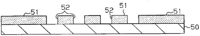
In the electrode pad of Japanese publication 2007-13092, remove support 60 and adjustment layer 61 with Wet-type etching, shown in Fig. 7 (a).Can etch away the periphery of electrode pad 62 like this, just, lead to the interface of insulating barrier 63, shown in Fig. 7 (b).In this case, between the periphery of electrode pad 62 and insulating barrier 63, form groove.The result is that electrode pad 62 is prone to from said groove layering with insulating barrier 63 or splits.
The purpose of this invention is to provide a kind of wiring substrate and manufacturing approach thereof, prevent that layering from appearring in the near interface between insulating barrier and electrode pad.
Summary of the invention
One aspect of the present invention provides the method that a kind of manufacturing has the wiring substrate of electrode pad.This method is included in and forms etchant resist on the support.This etchant resist is included in the opening that forms with the corresponding position of the formation part of the electrode pad of said wiring substrate.Said method further comprises, in the opening of said the above etchant resist of support, forms the adjustment layer.This adjustment layer comprises first flat surfaces that is arranged essentially parallel to said support, and first inclined surface that extends towards the sidewall of said opening from the edge of said first flat surfaces.Said method also is included in said adjustment layer and goes up the said electrode pad of formation.This electrode pad comprises periphery and middle body; Said periphery comprises corresponding second inclined surface of first inclined surface with said adjustment layer; Said middle body comprises and corresponding second flat surfaces of first flat surfaces of said adjustment layer that said middle body is recessed from said periphery.And then said method is included in and forms insulating barrier on the said support and on this insulating barrier, form wiring layer.This wiring layer is electrically coupled to said electrode pad.In addition, said method comprises and removes said support and said adjustment layer.
According to the method for above-mentioned manufacturing wiring substrate, when the said adjustment of etching layer, even want the periphery of the said electrode pad of etching, the distal end of said outstanding periphery becomes circle (rounded).Suppressed the etching at the interface between said electrode pad and said insulating barrier like this.Therefore, suppressed the said layering that occurs at the interface.
The further aspect of the present invention is a kind of wiring substrate of the electrode pad that comprises insulating barrier and come out from this insulating layer exposing.Said electrode pad comprises middle body, and this middle body comprises flat surfaces and periphery, and said middle body is recessed from said periphery.On said insulating barrier, arrange wiring layer, this wiring layer is electrically coupled to said electrode pad.
Others of the present invention and advantage combine accompanying drawing can become obvious from the description that hereinafter illustrates the principle of the invention.
Description of drawings
Next combine accompanying drawing to will be better appreciated by the present invention and purpose and advantage to the description of currently preferred embodiment through reference, wherein:
Fig. 1 shows the cross sectional view of wiring substrate according to an embodiment of the invention;
Fig. 2 is electrode pad and the cross section zoomed-in view on every side thereof that is presented in the wiring substrate of Fig. 1;
Fig. 3 (a) is the cross sectional view that shows the process of the wiring substrate that is used for shop drawings 1 to Fig. 3 (c) and 3 (e), and Fig. 3 (d) and 3 (f) are respectively the zoomed-in views of Fig. 3 (c) and 3 (e);
Fig. 4 (a) is the cross sectional view that shows the process of the wiring substrate that is used for shop drawings 1 to 4 (f);
Fig. 5 (a) to Fig. 5 (c) be the cross sectional view that shows overlay coating in another embodiment;
Fig. 6 (a) shows in another embodiment to 6 (c), is used to make the cross sectional view with process of the wiring substrate of formed overlay coating on the adjustment layer; And
Fig. 7 (a) and 7 (b) are the cross sectional view that shows the wiring substrate of prior art.
Embodiment
Refer now to Fig. 1 to Fig. 4 and describe one embodiment of the present of invention.
Fig. 1 has shown wiring substrate 10, comprises range upon range of first, second and the 3rd insulating barrier 20,30 and 40.In insulating barrier 20,30 and 40, form distribution 21,31 and 41 respectively. Insulating barrier 20,30 and 40 for example is to be formed by epoxy resin, and distribution 21,31 and 41 is to be formed such as copper by metal.
In first insulating barrier 20, form via hole 20a.Each first distribution 21 forms path 21a and Wiring pattern 21b, and path 21a is formed among each via hole 20a, and Wiring pattern 21b is connected to path 21a.Each second distribution 31 forms path 31a and Wiring pattern 31b with the mode identical with first distribution 21, and path 31a is formed among each via hole 30a of second insulating barrier 30, and Wiring pattern 31b is connected to path 31a.And then each the 3rd distribution 41 forms path 41a and Wiring pattern 41b, and path 41a is formed among each via hole 40a of the 3rd insulating barrier 40, and Wiring pattern 41b is connected to path 41a.
First insulating barrier 20 comprises recess 22, and it is corresponding to first distribution 21.Each recess 22 is circular, and diameter for example is 50 to 500 μ m.The cross sectional view of Fig. 1 to Fig. 4 is along the planar interception at the center that extends through recess 22.
As shown in Figure 2, in each recess 22 of first insulating barrier 20, form electrode pad 23.Electrode pad 23 comprises pad main body 24 and the lip-deep overlay coating 25 that is formed at pad main body 24.Pad main body 24 is to be made of copper.Overlay coating 25 comprises the nickel dam 25a that directly is formed on the pad main body 24, and is formed at the gold layer 25b on the nickel dam 25a.The thickness of pad main body 24 for example is 5 to 25 μ m.The thickness of nickel dam 25a for example is 0.005 to 0.5 μ m.Overlay coating 25 is not limited to nickel dam 25a and the such double-layer structure of gold layer 25b.For example; Overlay coating 25 can have the double-decker that comprises palladium layer 25c and gold layer 25b shown in Fig. 5 (a); The three-decker that comprises nickel dam 25a, palladium layer 25c and gold layer 25b shown in Fig. 5 (b), the perhaps single layer structure that comprises tin layer 25d shown in Fig. 5 (c).
The sidewall of the recess 22 that the electrode pad 23 that comprises flat 26 and ledge 27 and first insulating barrier 20 are interior contacts.Therefore, compare with the electrode pad that includes only flat, ledge 27 has increased the contact area with first insulating barrier 20.Improve the tackness between the electrode pad 23 and first insulating barrier 20 like this, suppressed the situation such as split at the interface between the electrode pad 23 and first insulating barrier 20.
What Fig. 2 showed is the soldered ball 28 that is connected to electrode pad 23.Electrode pad 23 is connected to semiconductor element pad (not shown) through soldered ball 28.
Described like preceding text, the periphery of electrode pad 23 has defined ledge 27.Therefore, soldered ball 28 is taken in by middle body (flat 26) easily, and said middle body is recessed from said periphery (ledge 27).And soldered ball 28 is being supported with ledge 27 by the flat 26 of electrode pad 23.Therefore, compare with the electrode pad that has only flat, the contact area between soldered ball 28 and the electrode pad 23 has increased.And the gap between the wall portion of soldered ball 28, electrode pad 23 and recess 22 reduces.Correspondingly, be applied to 28 last times of soldered ball as stress, the area (contact point) that electrode pad 23 usefulness of present embodiment are bigger supports soldered ball 28.So firmly support soldered ball 28.
In the present embodiment, the surface of electrode pad 23 is neither level and smooth curved surface, neither tabular surface, comprise the second flat surfaces 26a and the second inclined surface 27a.In addition, the interface between the second flat surfaces 26a and the second inclined surface 27a forms the bight.When electrode pad comprised level and smooth curved surface or tabular surface, stress can be applied to along the surface of said electrode pad on the soldered ball, may form crackle along said surface.Can propagate stress or crackle along the surface of said electrode pad like this.But in the present embodiment, the surface of electrode pad 23 is not a tabular surface.Therefore, for example, be applied to 28 last times of soldered ball as stress along the second inclined surface 27a, the near interface of stress between the second flat surfaces 26a and the second inclined surface 27a stops to propagate.
As shown in Figure 1, on the 3rd insulating barrier 40, form soldering-resistance layer 42.Soldering-resistance layer 42 comprises and the 3rd distribution 41 corresponding openings 43.Come out in the Wiring pattern 41b part of the 3rd distribution 41 like this.The 3rd distribution 41 electrically connects on the electrode of printed base plate.Like this semiconductor element is electrically connected through wiring substrate 10 with printed base plate and be in the same place.
With reference now to Fig. 3 and Fig. 4, the method for making wiring substrate 10 is described.
With reference to figure 3 (a), make wiring substrate 10, at first prepare support 50.Can be with sheet metal or tinsel as support 50.In the present embodiment, use Copper Foil.Then, with reference to figure 3 (b), on support 50, form etchant resist 51 (resist).For example, can use dry film as etchant resist 51.Etchant resist 51 is included in the formed opening 52 in the corresponding position of formation part with electrode pad 23.
With reference to figure 3 (c), in the opening 52 of etchant resist 51, form adjustment layer 53, be used for adjusting the shape of electrode pad 23.Adjustment layer 53 is through electroplating formation, electroplate with copper facing be plated to that the opening 52 of support 50 through etchant resist 51 come out that part of on.Therefore, adjustment layer 53 is formed by copper.Electroplate inorganic constituentss such as using copper sulphate, sulfuric acid and chlorine as electroplate liquid, and use organic principles such as equal paint (leveler), polymer and brightener as additive.The thickness of each adjustment layer 53 for example is 10 to 15 μ m, and is corresponding, as shown in Figure 2 to the distance L 1 of the second flat surfaces 26a (electrode pad 23) with the top (first insulating barrier 20) from recess 22.The thickness of each adjustment layer 53 is less than the degree of depth of each opening 52.
Composition through the adjustment plating bath obtains the smooth coating in the central portion office of each opening 52.Correspondingly; In the present embodiment; As shown in Figure 3; Formed each adjustment layer 53 comprise the first flat surfaces 53a (first flat surfaces) of the lower surface that is arranged essentially parallel to corresponding opening 52 and from the edge of the first flat surfaces 53a towards support 50 extend, up to the first inclined surface 53b (first inclined surface) of the wall portion of opening 52.Therefore, the first flat surfaces 53a of adjustment layer 53 is corresponding to the second flat surfaces 26a of electrode pad 23.In addition, the first inclined surface 53b of adjustment layer 53 is corresponding to the second inclined surface 27a of electrode pad 23.In the example shown in Fig. 3 (d), the cross section of adjustment layer 53 is hexagons.But when plating is when carrying out at short notice, the first inclined surface 53b is near support 50.Therefore, the cross section of adjustment layer 53 can be trapezoidal.By this way, between the wall portion of first inclined surface 53b that adjusts layer 53 and opening 52, form the groove 54 that cross section is substantially V-arrangement.
With reference to figure 3 (e), on the surface of each adjustment layer 53, form the pad main body 24 of electrode pad 23.In the present embodiment, with reference to figure 3 (f), on the surface of each adjustment layer 53, forming thickness is the nickel dam 55 of 0.05 to 10 μ m.Implementing copper facing then is the pad main body 24 of 5 to 25 μ m to form thickness.Shown in Fig. 3 (f), nickel dam 55 forms and shaping along the surface of adjustment layer 53, and therefore formed pad main body 24 comprises flat surfaces 24a (second flat surfaces) and inclined surface 24b (second inclined surface).
Then, with reference to figure 4 (a), removed etchant resist 51.And then pad main body 24 is carried out surface roughening with support 50 and is handled the surface roughness of acquisition 0.5 to 2 μ m.Carry out surface roughening and handle, make in the ensuing PROCESS FOR TREATMENT shown in Fig. 4 (b), first insulating barrier 20 adheres on support 50 and the pad main body 24 easily.Can carry out anisotropic etching (for example, Wet-type etching) and carry out said roughened.
In the technology shown in Fig. 4 (b), carry out lamination process and on the surface of support 50, form first insulating barrier 20, cover pad main body 24.More specifically, at support 50 laminated resin moldings.Heat-treat when pushing said resin molding.Then, said resin molding is solidified to form first insulating barrier 20.With reference to figure 4 (c), for example,, form via hole 20a with corresponding that part of of laser beam irradiation first insulating barrier 20 and pad main body 24, and exposed pad main body 24.Then,, in each via hole 20a, for example become technology, form first distribution 21 through carrying out false add with reference to figure 4 (d).
With reference to figure 4 (e), form second insulating barrier 30 and second distribution 31 in the same way.Form the 3rd insulating barrier 40 and the 3rd distribution 41 then in the same way.Obtain Wiring construction element like this.The surface coverage of the 3rd insulating barrier 40 has soldering-resistance layer 42, with the 3rd distribution 41 corresponding formation openings 43.A kind of first to the 3rd insulating barrier 20,30 and 40 and the formation method of the Wiring construction element of distribution 21,31 and 41 of comprising except false add becomes technology, can be used picture to subtract into various types of distributions such as technology (sub-tractive process) and form technologies.
With reference to figure 4 (f), for example, remove support 50 and adjustment layer 53 with Wet-type etching.Then, etching nickel dam 55 is with exposed pad main body 24.When the pad main body only comprised flat surfaces, the sidewall of each recess 22 in first insulating barrier 20 at right angles contacted with the surface of corresponding bonding pad main body substantially.In the present embodiment, the periphery of pad main body 24 is defined by inclined surface 24b.Therefore, the sidewall of each recess 22 in first insulating barrier 20 contacts with the surface of corresponding bonding pad main body 24 in obtuse angle.The result is, etching solution can not remain in each pad main body 24 periphery near.And then, or even when etching away pad main body 24, the distal end of inclined surface 24b can be only circular.Suppressed the corrosion at the interface between the pad main body 24 and first insulating barrier 20 by this way.
At last, under the state that pad main body 24 comes out, with reference to shown in Figure 2, carry out chemical plating (electroless plating), butt welding disc main body 24 carries out surface treatment, forms nickel dam 25a and gold layer 25b in order.Said surface treatment is not limited to and forms the overlay coating 25 that comprises nickel dam 25a and gold layer 25b.For example, can carry out chemical plating forms on the surface of pad main body 24 and comprises nickel dam, palladium layer and gold layer this overlay coating of three layers (Fig. 5 (b)).Can also carry out chemical plating, formation comprises palladium layer and gold layer this two layers of surface coating (Fig. 5 (a)) on the surface of pad main body 24.In addition, can also carry out chemical plating, on the surface of pad main body 24, form the overlay coating (Fig. 5 (c)) that includes only tin.Can carry out organic solderability preservative (OSB) technology and on the surface of pad main body 24, form the oxidation-resistant film that forms by organic principle.Form electrode pad 23 like this.Make wiring substrate 10 by this way.
The advantage of present embodiment is described now.
(1) when making wiring substrate 10; Adjustment layer 53 comprises the first flat surfaces 53a that is arranged essentially parallel to support 50, and extend towards the surface of support 50 from the edge of the first flat surfaces 53a, the first inclined surface 53b of the wall portion of the respective openings 52 up to etchant resist 51.The result is, the pad main body 24 that is formed on the adjustment layer 53 comprises the flat surfaces 24a of the surperficial corresponding middle body that is arranged on and adjusts layer 53, and be arranged on periphery, from the outstanding outwardly inclined surface 24b of said middle body.Correspondingly, when etching support 50 and adjustment layer 53,, comprise that the distal end of the outstanding periphery of inclined surface 24b can be only circular even want the part of etching pad main body 24.Suppressed the corrosion at the interface between the pad main body 24 and first insulating barrier 20 like this.And then, because can corroding electrode pad 23 and first insulating barrier 20 between the interface, suppressed to occur layering at the interface said.
(2) in wiring substrate 10, electrode pad 23 is arranged in each recess 22, and recess 22 is formed in the surface of first insulating barrier 20.Electrode pad 23 comprises flat 26 with second flat surfaces 26a and the ledge 27 with second inclined surface 27a.Owing to comprise that the electrode pad 23 of flat 26 and ledge 27 contacts with first insulating barrier 20, to compare with the electrode pad that only comprises flat, ledge 27 has increased the contact area with first insulating barrier 20.Improve the tackness between the electrode pad 23 and first insulating barrier 20 like this, suppressed the cracking at the interface between the electrode pad 23 and first insulating barrier 20.
(3) electrode pad 23 that comprises flat 26 and ledge 27 is connected on the soldered ball 28.Therefore, soldered ball 28 is received to the middle body of electrode pad 23 easily, only comprises that with electrode pad flat compares, and the contact area between soldered ball 28 and the electrode pad 23 increases.Improved the stability of soldered ball 28 like this, electrode pad 23 further stably supports soldered ball 28.
It will be apparent for a person skilled in the art that under the situation that does not depart from category of the present invention the present invention can be presented as many other concrete forms.Particularly it is to be understood that the present invention can be presented as following form.
In the above-described embodiments, in the technology shown in Fig. 3 (e), pad main body 24 is after the surface of adjustment layer 53 forms nickel dam 55, to form.In addition, remove in the technology, after removing support 50, adjustment layer 53 and nickel dam 55, on pad main body 24, form overlay coating 25 at support shown in Figure 4.In a further embodiment, in the technology that is used to form electrode pad 23 shown in Fig. 3 (e), pad main body 24 is on adjustment layer 53, to form after the position formation overlay coating 25 corresponding to nickel dam 55.In addition, remove in the technology, only remove support 50 and adjustment layer 53 at the support of Fig. 4 (f).In this case, formed overlay coating 25.Therefore, do not need again will after the technology of Fig. 4 (f), on pad main body 24, to form overlay coating 25 as in the above-described embodiments.Reduced manufacturing step like this.The overlay coating 25 that is formed on the adjustment layer 53 can be for example to comprise the three laminar surface coating of gold layer 25b (0.005 to 0.5 μ m), palladium layer 25c (0.005 to 0.5 μ m) and nickel dam 25a (0.5 to 10 μ m), shown in Fig. 6 (a).Overlay coating 25 can also be the double-deck overlay coating that comprises gold layer 25b (0.005 to 0.5 μ m) and nickel dam 25a (0.5 to 10 μ m), shown in Fig. 6 (b).Interchangeable is that overlay coating 25 can be the double-deck overlay coating that comprises gold layer 25b (0.005 to 0.5 μ m) and palladium layer 25c (0.005 to 0.5 μ m), shown in Fig. 6 (c).
In the above embodiments, electrode pad 23 comprises flat 26 and ledge 27.In addition, as shown in Figure 2, the second inclined surface 27a of ledge 27 is smooth.But the shape of ledge 27 is unrestricted.For example, the surface of ledge 27 can be circular, rather than smooth.In this case, preferably form the bight in the interface between the flat surfaces of the surface of ledge and flat.The advantage (4) that has the foregoing description like this.
In the wiring substrate 10 of the foregoing description, electrode pad 23 is to be connected on the semiconductor element electrode pad through soldered ball 28.But electrode pad 23 can be connected on the semiconductor element through metal wire.
In the wiring substrate 10 of the foregoing description, electrode pad 23 is to be connected to semiconductor element through soldered ball 28, and printed base plate is connected to the 3rd insulating barrier 40 of wiring substrate 10.But said printed base plate can be connected on the electrode pad 23, and semiconductor element can be connected on the 3rd distribution 41, just, and the soldering-resistance layer 42 that comes out from opening 43 that part of.
In the manufacturing approach of the foregoing description, after forming pad main body 24, after removing etchant resist 51, form first insulating barrier 20.But, can not remove etchant resist 51 and form first insulating barrier 20.In this case, electrode pad 23 is formed on the wiring substrate of manufacturing, is arranged in the corresponding opening 52 in the surface of etchant resist 51.
In the above-described embodiments, use the material of epoxy resin, with the material of the pad main body of copper conduct in each electrode pad and the material of distribution as insulating barrier.But, can use other as the material of polyimide resin and so on as insulating barrier, the material of said pad main body and distribution is not limited to copper, can change.In addition, thickness of the size of the size of formed recess, electrode pad, each layer and Wiring pattern are unrestricted in said insulating barrier.The number of range upon range of insulating barrier is also unrestricted.In addition, during manufacture, said support is not limited to copper with the used material of adjustment layer, can change.In addition, only need said adjustment layer be formed and comprise flat surfaces and inclined surface.The etchant resist and the plating bath that are used to form said adjustment layer are unrestricted, and the technology that is used to form said adjustment layer is unrestricted.For example, after forming complete, smooth adjustment layer, periphery that can the said adjustment layer of etching is to form said inclined surface.In addition, can form said adjustment layer except that other technology electroplating.In this case, said technology is not limited to aforesaid description.
All examples that this paper put down in writing and conditional statement are intended to instruction; For principle of the present invention and the design that helps reader understanding inventor that the technology in-depth is proposed; Be to be understood that the example that do not receive to enumerate especially for the present invention and the restriction of condition here, and in the specification these examples tissue with show that Pros and Cons of the present invention is irrelevant.Though described embodiments of the invention in detail, should be understood that, under the situation that does not depart from spirit of the present invention and category, can carry out various changes, displacement and replacement to it.
Claims (10)
1. method that is used to make the wiring substrate that comprises electrode pad, this method comprises:
On support, form etchant resist, wherein this etchant resist comprises opening, and this opening is forming the corresponding position of part with the electrode pad of said wiring substrate;
In the opening of said the above etchant resist of support, form the adjustment layer; Wherein said adjustment layer comprises first flat surfaces that is arranged essentially parallel to said support, and first inclined surface that extends towards the sidewall of said opening from the edge of said first flat surfaces;
On said adjustment layer, form said electrode pad; Wherein said electrode pad comprises periphery and middle body; Said periphery comprises corresponding second inclined surface of first inclined surface with said adjustment layer; Said middle body comprises and corresponding second flat surfaces of first flat surfaces of said adjustment layer that said middle body is recessed from said periphery;
On said support, form insulating barrier;
On said insulating barrier, form wiring layer, wherein said wiring layer electrically connects on said electrode pad; And
Remove said support and said adjustment layer.
2. method according to claim 1 also is included in and removes after said support and the said adjustment layer, on said electrode pad, forms overlay coating.
3. method according to claim 1, the said electrode pad of wherein said formation are included in said adjustment layer and go up the formation overlay coating, and on said overlay coating, form the electrode pad main body.
4. method according to claim 1 also is included in after the said electrode pad of formation, on said electrode pad, carries out roughening technology.
5. method according to claim 1, wherein said adjustment layer forms through plating.
6. method according to claim 1, wherein said periphery comprises smooth basically distal end.
7. wiring substrate comprises:
Insulating barrier;
From the electrode pad that said insulating layer exposing is come out, wherein said electrode pad comprises middle body and periphery, and said middle body comprises flat surfaces, and said middle body is recessed from said periphery; And
Be arranged on the said insulating barrier and electrically connect the wiring layer on said electrode pad.
8. wiring substrate according to claim 7, wherein said electrode pad comprise the pad main body and are formed at the overlay coating on the said pad main body.
9. wiring substrate according to claim 7, wherein said periphery comprises smooth basically distal end.
10. wiring substrate comprises:
Insulating barrier with recess, wherein said recess comprises the lower surface with opening;
Electrode pad; It forms on the lower surface of the recess of said insulating barrier to cover said opening; Wherein said electrode pad comprises middle body and periphery; Said middle body comprises the flat surfaces that is arranged essentially parallel to said insulating barrier, and said periphery comprises the inclined surface that extends from the sidewall of the said opening of edge court of said middle body, and said middle body is recessed from said periphery; And
Be formed at the wiring layer on the said insulating barrier, wherein said wiring layer is electrically coupled to said electrode pad through the opening in the said lower surface.
Applications Claiming Priority (2)
| Application Number | Priority Date | Filing Date | Title |
|---|---|---|---|
| JP2010155785A JP5502624B2 (en) | 2010-07-08 | 2010-07-08 | Wiring board manufacturing method and wiring board |
| JP2010-155785 | 2010-07-08 |
Publications (1)
| Publication Number | Publication Date |
|---|---|
| CN102316680A true CN102316680A (en) | 2012-01-11 |
Family
ID=45429376
Family Applications (1)
| Application Number | Title | Priority Date | Filing Date |
|---|---|---|---|
| CN2011101979171A Pending CN102316680A (en) | 2010-07-08 | 2011-07-06 | The method of wiring substrate and manufacturing wiring substrate |
Country Status (5)
| Country | Link |
|---|---|
| US (1) | US20120006591A1 (en) |
| JP (1) | JP5502624B2 (en) |
| KR (1) | KR20120005383A (en) |
| CN (1) | CN102316680A (en) |
| TW (1) | TWI521618B (en) |
Cited By (1)
| Publication number | Priority date | Publication date | Assignee | Title |
|---|---|---|---|---|
| CN113348548A (en) * | 2019-01-30 | 2021-09-03 | 京瓷株式会社 | Electronic component mounting substrate and electronic device |
Families Citing this family (19)
| Publication number | Priority date | Publication date | Assignee | Title |
|---|---|---|---|---|
| JP5142967B2 (en) * | 2008-12-10 | 2013-02-13 | ルネサスエレクトロニクス株式会社 | Semiconductor device |
| JP6166879B2 (en) * | 2011-09-06 | 2017-07-19 | 株式会社 大昌電子 | Single-sided printed wiring board and manufacturing method thereof |
| US20130168132A1 (en) * | 2011-12-29 | 2013-07-04 | Sumsung Electro-Mechanics Co., Ltd. | Printed circuit board and method of manufacturing the same |
| JP6110084B2 (en) * | 2012-07-06 | 2017-04-05 | 株式会社 大昌電子 | Printed wiring board and manufacturing method thereof |
| WO2014071815A1 (en) * | 2012-11-08 | 2014-05-15 | 南通富士通微电子股份有限公司 | Semiconductor device and manufacturing method thereof |
| CN102915986B (en) | 2012-11-08 | 2015-04-01 | 南通富士通微电子股份有限公司 | Chip packaging structure |
| WO2014071813A1 (en) | 2012-11-08 | 2014-05-15 | 南通富士通微电子股份有限公司 | Semiconductor device package and packaging method |
| KR101411813B1 (en) | 2012-11-09 | 2014-06-27 | 앰코 테크놀로지 코리아 주식회사 | Semiconductor device and manufacturing method thereof |
| KR101516083B1 (en) * | 2013-10-14 | 2015-04-29 | 삼성전기주식회사 | Printed circuit board and method of manufacturing the same |
| US9412686B2 (en) * | 2014-08-26 | 2016-08-09 | United Microelectronics Corp. | Interposer structure and manufacturing method thereof |
| JP2016076534A (en) * | 2014-10-03 | 2016-05-12 | イビデン株式会社 | Printed wiring board with metal post and method of manufacturing the same |
| KR101896226B1 (en) * | 2015-05-15 | 2018-10-18 | 스템코 주식회사 | Flexible printed circuit board and method for manufacturing the same |
| KR102040605B1 (en) | 2015-07-15 | 2019-12-05 | 엘지이노텍 주식회사 | The printed circuit board and the method for manufacturing the same |
| KR102326505B1 (en) | 2015-08-19 | 2021-11-16 | 엘지이노텍 주식회사 | The printed circuit board and the method for manufacturing the same |
| KR101742433B1 (en) * | 2016-04-21 | 2017-05-31 | 엘지이노텍 주식회사 | The printed circuit board and the method for manufacturing the same |
| TWI576033B (en) * | 2016-05-06 | 2017-03-21 | 旭德科技股份有限公司 | Circuit substrate and manufacturing method thereof |
| JP6615701B2 (en) * | 2016-06-24 | 2019-12-04 | 新光電気工業株式会社 | WIRING BOARD, SEMICONDUCTOR DEVICE, AND WIRING BOARD MANUFACTURING METHOD |
| KR102119807B1 (en) * | 2018-02-13 | 2020-06-05 | 엘지이노텍 주식회사 | The printed circuit board and the method for manufacturing the same |
| JP2021093417A (en) * | 2019-12-09 | 2021-06-17 | イビデン株式会社 | Print circuit board and manufacturing method of print circuit board |
Citations (5)
| Publication number | Priority date | Publication date | Assignee | Title |
|---|---|---|---|---|
| JP2000165024A (en) * | 1998-11-25 | 2000-06-16 | Kyocera Corp | Wiring board, electronic component and their connecting method |
| CN1491076A (en) * | 2002-09-17 | 2004-04-21 | �¹������ҵ��ʽ���� | Method for preparing wiring placode |
| JP2009065114A (en) * | 2008-05-12 | 2009-03-26 | Shinko Electric Ind Co Ltd | Manufacturing method of circuit board, and the circuit board |
| JP2009064973A (en) * | 2007-09-06 | 2009-03-26 | Shinko Electric Ind Co Ltd | Manufacturing method of wiring board |
| US20100139963A1 (en) * | 2008-12-10 | 2010-06-10 | Nec Electronics Corporation | Interconnect substrate, method of manufacturing interconnect substrate and semiconductor device |
Family Cites Families (5)
| Publication number | Priority date | Publication date | Assignee | Title |
|---|---|---|---|---|
| US6586843B2 (en) * | 2001-11-08 | 2003-07-01 | Intel Corporation | Integrated circuit device with covalently bonded connection structure |
| JP4146864B2 (en) * | 2005-05-31 | 2008-09-10 | 新光電気工業株式会社 | WIRING BOARD AND MANUFACTURING METHOD THEREOF, SEMICONDUCTOR DEVICE AND SEMICONDUCTOR DEVICE MANUFACTURING METHOD |
| TWI331494B (en) * | 2007-03-07 | 2010-10-01 | Unimicron Technology Corp | Circuit board structure |
| JP5101169B2 (en) * | 2007-05-30 | 2012-12-19 | 新光電気工業株式会社 | Wiring board and manufacturing method thereof |
| KR101070022B1 (en) * | 2009-09-16 | 2011-10-04 | 삼성전기주식회사 | Multi-layer ceramic circuit board, fabrication method of the same and electric device module |
-
2010
- 2010-07-08 JP JP2010155785A patent/JP5502624B2/en active Active
-
2011
- 2011-07-04 KR KR1020110065762A patent/KR20120005383A/en not_active Application Discontinuation
- 2011-07-04 TW TW100123500A patent/TWI521618B/en active
- 2011-07-06 CN CN2011101979171A patent/CN102316680A/en active Pending
- 2011-07-06 US US13/176,876 patent/US20120006591A1/en not_active Abandoned
Patent Citations (5)
| Publication number | Priority date | Publication date | Assignee | Title |
|---|---|---|---|---|
| JP2000165024A (en) * | 1998-11-25 | 2000-06-16 | Kyocera Corp | Wiring board, electronic component and their connecting method |
| CN1491076A (en) * | 2002-09-17 | 2004-04-21 | �¹������ҵ��ʽ���� | Method for preparing wiring placode |
| JP2009064973A (en) * | 2007-09-06 | 2009-03-26 | Shinko Electric Ind Co Ltd | Manufacturing method of wiring board |
| JP2009065114A (en) * | 2008-05-12 | 2009-03-26 | Shinko Electric Ind Co Ltd | Manufacturing method of circuit board, and the circuit board |
| US20100139963A1 (en) * | 2008-12-10 | 2010-06-10 | Nec Electronics Corporation | Interconnect substrate, method of manufacturing interconnect substrate and semiconductor device |
Cited By (1)
| Publication number | Priority date | Publication date | Assignee | Title |
|---|---|---|---|---|
| CN113348548A (en) * | 2019-01-30 | 2021-09-03 | 京瓷株式会社 | Electronic component mounting substrate and electronic device |
Also Published As
| Publication number | Publication date |
|---|---|
| KR20120005383A (en) | 2012-01-16 |
| US20120006591A1 (en) | 2012-01-12 |
| JP5502624B2 (en) | 2014-05-28 |
| TW201209945A (en) | 2012-03-01 |
| TWI521618B (en) | 2016-02-11 |
| JP2012019080A (en) | 2012-01-26 |
Similar Documents
| Publication | Publication Date | Title |
|---|---|---|
| CN102316680A (en) | The method of wiring substrate and manufacturing wiring substrate | |
| US9693458B2 (en) | Printed wiring board, method for manufacturing printed wiring board and package-on-package | |
| JP2008263125A5 (en) | ||
| JP2007013092A5 (en) | ||
| CN1819746A (en) | Wired circuit board and producing method thereof | |
| US20120164854A1 (en) | Packaging substrate and method of fabricating the same | |
| TWI711357B (en) | Electronic module and circuit board | |
| TW201019445A (en) | Lead frame board, method of forming the same, and semiconductor device | |
| WO2011158731A1 (en) | Substrate for mounting semiconductor element and method for manufacturing the substrate | |
| JP2008021739A (en) | Method for manufacturing substrate | |
| US20200365418A1 (en) | Printed wiring board and method for manufacturing printed wiring board | |
| JP2010062517A (en) | Nickel-gold plating method and printed circuit board | |
| US8552303B2 (en) | Circuit structure and manufacturing method thereof | |
| CN102005427B (en) | Printed circuit board strip and panel | |
| US20220330428A1 (en) | Printed wiring board and method for manufacturing the same | |
| US8786108B2 (en) | Package structure | |
| CN111696956B (en) | Porous Cu on Cu surface for semiconductor packages | |
| JP4326014B2 (en) | Circuit board and manufacturing method thereof | |
| TW202019248A (en) | Connecting structure and method for connecting stacked circuits boards using the same | |
| KR101162506B1 (en) | Printed circuit board and method for manufacturing the same | |
| US20140331493A1 (en) | Method of fabricating a package substrate | |
| JP2002260753A (en) | Manufacturing method of sheets with bumps | |
| US20130233602A1 (en) | Surface treatment structure of circuit pattern | |
| JP2021103733A (en) | Printed circuit board and method of manufacturing printed circuit board | |
| CN101930928B (en) | Manufacturing method of thin base plate for packaging semiconductor |
Legal Events
| Date | Code | Title | Description |
|---|---|---|---|
| C06 | Publication | ||
| PB01 | Publication | ||
| C10 | Entry into substantive examination | ||
| SE01 | Entry into force of request for substantive examination | ||
| C02 | Deemed withdrawal of patent application after publication (patent law 2001) | ||
| WD01 | Invention patent application deemed withdrawn after publication |
Application publication date: 20120111 |