CN101903979B - 组合喷淋头电极总成、连接其各部件的方法及衬底处理方法 - Google Patents
组合喷淋头电极总成、连接其各部件的方法及衬底处理方法 Download PDFInfo
- Publication number
- CN101903979B CN101903979B CN200880123061XA CN200880123061A CN101903979B CN 101903979 B CN101903979 B CN 101903979B CN 200880123061X A CN200880123061X A CN 200880123061XA CN 200880123061 A CN200880123061 A CN 200880123061A CN 101903979 B CN101903979 B CN 101903979B
- Authority
- CN
- China
- Prior art keywords
- electrode
- face
- electrode assembly
- bonding die
- supporting member
- Prior art date
- Legal status (The legal status is an assumption and is not a legal conclusion. Google has not performed a legal analysis and makes no representation as to the accuracy of the status listed.)
- Active
Links
- 239000002131 composite material Substances 0.000 title claims abstract description 39
- 238000000034 method Methods 0.000 title claims description 57
- 239000000758 substrate Substances 0.000 title claims description 27
- 238000003672 processing method Methods 0.000 title 1
- 239000000853 adhesive Substances 0.000 claims abstract description 137
- 230000001070 adhesive effect Effects 0.000 claims abstract description 137
- 238000012545 processing Methods 0.000 claims abstract description 34
- 239000000945 filler Substances 0.000 claims abstract description 23
- 229920001296 polysiloxane Polymers 0.000 claims abstract description 20
- 230000000704 physical effect Effects 0.000 claims abstract description 8
- 125000000118 dimethyl group Chemical group [H]C([H])([H])* 0.000 claims abstract description 7
- 239000013464 silicone adhesive Substances 0.000 claims abstract description 5
- 239000000463 material Substances 0.000 claims description 44
- 230000008569 process Effects 0.000 claims description 23
- 229910052710 silicon Inorganic materials 0.000 claims description 17
- 239000010703 silicon Substances 0.000 claims description 17
- XUIMIQQOPSSXEZ-UHFFFAOYSA-N Silicon Chemical compound [Si] XUIMIQQOPSSXEZ-UHFFFAOYSA-N 0.000 claims description 16
- 238000004026 adhesive bonding Methods 0.000 claims description 13
- 238000012546 transfer Methods 0.000 claims description 13
- 239000004411 aluminium Substances 0.000 claims description 11
- 229910052782 aluminium Inorganic materials 0.000 claims description 11
- 239000012530 fluid Substances 0.000 claims description 10
- XAGFODPZIPBFFR-UHFFFAOYSA-N aluminium Chemical group [Al] XAGFODPZIPBFFR-UHFFFAOYSA-N 0.000 claims description 9
- OKTJSMMVPCPJKN-UHFFFAOYSA-N Carbon Chemical compound [C] OKTJSMMVPCPJKN-UHFFFAOYSA-N 0.000 claims description 8
- 229910010271 silicon carbide Inorganic materials 0.000 claims description 8
- 239000004065 semiconductor Substances 0.000 claims description 7
- 230000008859 change Effects 0.000 claims description 6
- 238000006243 chemical reaction Methods 0.000 claims description 6
- 238000005520 cutting process Methods 0.000 claims description 6
- 229910002804 graphite Inorganic materials 0.000 claims description 6
- 239000010439 graphite Substances 0.000 claims description 6
- 230000008676 import Effects 0.000 claims description 6
- 229910021421 monocrystalline silicon Inorganic materials 0.000 claims description 6
- 238000005530 etching Methods 0.000 claims description 5
- 238000003475 lamination Methods 0.000 claims description 5
- 238000007711 solidification Methods 0.000 claims description 5
- 230000008023 solidification Effects 0.000 claims description 5
- PNEYBMLMFCGWSK-UHFFFAOYSA-N Alumina Chemical compound [O-2].[O-2].[O-2].[Al+3].[Al+3] PNEYBMLMFCGWSK-UHFFFAOYSA-N 0.000 claims description 4
- 238000004132 cross linking Methods 0.000 claims description 4
- 238000011049 filling Methods 0.000 claims description 4
- 238000012423 maintenance Methods 0.000 claims description 4
- 239000002245 particle Substances 0.000 claims description 4
- 230000003068 static effect Effects 0.000 claims description 4
- PZNSFCLAULLKQX-UHFFFAOYSA-N Boron nitride Chemical compound N#B PZNSFCLAULLKQX-UHFFFAOYSA-N 0.000 claims description 3
- 229910045601 alloy Inorganic materials 0.000 claims description 3
- 239000000956 alloy Substances 0.000 claims description 3
- 230000008602 contraction Effects 0.000 claims description 3
- 239000011521 glass Substances 0.000 claims description 3
- 239000000203 mixture Substances 0.000 claims description 3
- 150000002978 peroxides Chemical class 0.000 claims description 3
- 238000007725 thermal activation Methods 0.000 claims description 3
- 230000006835 compression Effects 0.000 claims description 2
- 238000007906 compression Methods 0.000 claims description 2
- 239000003365 glass fiber Substances 0.000 claims description 2
- 239000002102 nanobead Substances 0.000 claims description 2
- TWNQGVIAIRXVLR-UHFFFAOYSA-N oxo(oxoalumanyloxy)alumane Chemical compound O=[Al]O[Al]=O TWNQGVIAIRXVLR-UHFFFAOYSA-N 0.000 claims description 2
- 229910021420 polycrystalline silicon Inorganic materials 0.000 claims description 2
- 229920005591 polysilicon Polymers 0.000 claims description 2
- 230000008021 deposition Effects 0.000 claims 2
- 230000005489 elastic deformation Effects 0.000 claims 2
- 238000003698 laser cutting Methods 0.000 claims 2
- 229910052582 BN Inorganic materials 0.000 claims 1
- 230000000295 complement effect Effects 0.000 claims 1
- 238000009434 installation Methods 0.000 abstract description 3
- 230000013011 mating Effects 0.000 abstract 3
- 230000001351 cycling effect Effects 0.000 abstract 1
- 239000007789 gas Substances 0.000 description 57
- 239000011230 binding agent Substances 0.000 description 25
- 229920001971 elastomer Polymers 0.000 description 23
- 239000000806 elastomer Substances 0.000 description 22
- 239000013536 elastomeric material Substances 0.000 description 17
- 230000035882 stress Effects 0.000 description 16
- 239000007788 liquid Substances 0.000 description 13
- 238000012360 testing method Methods 0.000 description 11
- 239000007921 spray Substances 0.000 description 10
- 239000003344 environmental pollutant Substances 0.000 description 7
- 238000009832 plasma treatment Methods 0.000 description 7
- 231100000719 pollutant Toxicity 0.000 description 7
- 238000010008 shearing Methods 0.000 description 7
- 238000005516 engineering process Methods 0.000 description 5
- 238000009661 fatigue test Methods 0.000 description 5
- 239000003517 fume Substances 0.000 description 5
- 229910052751 metal Inorganic materials 0.000 description 5
- 239000002184 metal Substances 0.000 description 5
- 229910000838 Al alloy Inorganic materials 0.000 description 4
- 230000008878 coupling Effects 0.000 description 4
- 238000010168 coupling process Methods 0.000 description 4
- 238000005859 coupling reaction Methods 0.000 description 4
- 239000013078 crystal Substances 0.000 description 4
- 150000002500 ions Chemical class 0.000 description 4
- 238000002360 preparation method Methods 0.000 description 4
- PXHVJJICTQNCMI-UHFFFAOYSA-N Nickel Chemical group [Ni] PXHVJJICTQNCMI-UHFFFAOYSA-N 0.000 description 3
- -1 and high-purity Inorganic materials 0.000 description 3
- 230000000712 assembly Effects 0.000 description 3
- 238000000429 assembly Methods 0.000 description 3
- 230000004888 barrier function Effects 0.000 description 3
- 230000007797 corrosion Effects 0.000 description 3
- 238000005260 corrosion Methods 0.000 description 3
- 238000010586 diagram Methods 0.000 description 3
- 239000004642 Polyimide Substances 0.000 description 2
- 239000004809 Teflon Substances 0.000 description 2
- 229920006362 Teflon® Polymers 0.000 description 2
- RTAQQCXQSZGOHL-UHFFFAOYSA-N Titanium Chemical compound [Ti] RTAQQCXQSZGOHL-UHFFFAOYSA-N 0.000 description 2
- 150000001398 aluminium Chemical class 0.000 description 2
- 230000008901 benefit Effects 0.000 description 2
- 230000015572 biosynthetic process Effects 0.000 description 2
- 238000009954 braiding Methods 0.000 description 2
- 239000004568 cement Substances 0.000 description 2
- 238000005229 chemical vapour deposition Methods 0.000 description 2
- 230000004087 circulation Effects 0.000 description 2
- 238000004140 cleaning Methods 0.000 description 2
- 239000011231 conductive filler Substances 0.000 description 2
- 239000004020 conductor Substances 0.000 description 2
- 229920001577 copolymer Polymers 0.000 description 2
- 239000003431 cross linking reagent Substances 0.000 description 2
- 230000002950 deficient Effects 0.000 description 2
- 238000009826 distribution Methods 0.000 description 2
- 239000003292 glue Substances 0.000 description 2
- 238000010438 heat treatment Methods 0.000 description 2
- 239000012535 impurity Substances 0.000 description 2
- 238000004519 manufacturing process Methods 0.000 description 2
- 229910003465 moissanite Inorganic materials 0.000 description 2
- 238000005240 physical vapour deposition Methods 0.000 description 2
- 238000001020 plasma etching Methods 0.000 description 2
- 229920001721 polyimide Polymers 0.000 description 2
- BFKJFAAPBSQJPD-UHFFFAOYSA-N tetrafluoroethene Chemical compound FC(F)=C(F)F BFKJFAAPBSQJPD-UHFFFAOYSA-N 0.000 description 2
- 239000010936 titanium Substances 0.000 description 2
- 229910052719 titanium Inorganic materials 0.000 description 2
- OVSKIKFHRZPJSS-UHFFFAOYSA-N 2,4-D Chemical compound OC(=O)COC1=CC=C(Cl)C=C1Cl OVSKIKFHRZPJSS-UHFFFAOYSA-N 0.000 description 1
- LLYXJBROWQDVMI-UHFFFAOYSA-N 2-chloro-4-nitrotoluene Chemical compound CC1=CC=C([N+]([O-])=O)C=C1Cl LLYXJBROWQDVMI-UHFFFAOYSA-N 0.000 description 1
- RYGMFSIKBFXOCR-UHFFFAOYSA-N Copper Chemical compound [Cu] RYGMFSIKBFXOCR-UHFFFAOYSA-N 0.000 description 1
- 241000221931 Hypomyces rosellus Species 0.000 description 1
- ZOKXTWBITQBERF-UHFFFAOYSA-N Molybdenum Chemical compound [Mo] ZOKXTWBITQBERF-UHFFFAOYSA-N 0.000 description 1
- 239000004695 Polyether sulfone Substances 0.000 description 1
- 230000004913 activation Effects 0.000 description 1
- 238000001994 activation Methods 0.000 description 1
- 239000012190 activator Substances 0.000 description 1
- 230000032683 aging Effects 0.000 description 1
- 230000005540 biological transmission Effects 0.000 description 1
- 229910052799 carbon Inorganic materials 0.000 description 1
- 238000005266 casting Methods 0.000 description 1
- 229920002678 cellulose Polymers 0.000 description 1
- 239000001913 cellulose Substances 0.000 description 1
- 239000003795 chemical substances by application Substances 0.000 description 1
- 238000004891 communication Methods 0.000 description 1
- 229910052802 copper Inorganic materials 0.000 description 1
- 239000010949 copper Substances 0.000 description 1
- 229910052593 corundum Inorganic materials 0.000 description 1
- 238000013461 design Methods 0.000 description 1
- 239000006185 dispersion Substances 0.000 description 1
- 238000001035 drying Methods 0.000 description 1
- 239000000428 dust Substances 0.000 description 1
- 230000005684 electric field Effects 0.000 description 1
- 239000000835 fiber Substances 0.000 description 1
- 229920002313 fluoropolymer Polymers 0.000 description 1
- 239000004811 fluoropolymer Substances 0.000 description 1
- 230000006870 function Effects 0.000 description 1
- 229910021389 graphene Inorganic materials 0.000 description 1
- 238000002347 injection Methods 0.000 description 1
- 239000007924 injection Substances 0.000 description 1
- 238000007641 inkjet printing Methods 0.000 description 1
- 238000010030 laminating Methods 0.000 description 1
- 238000003754 machining Methods 0.000 description 1
- 230000007246 mechanism Effects 0.000 description 1
- 229910001092 metal group alloy Inorganic materials 0.000 description 1
- 230000005012 migration Effects 0.000 description 1
- 238000013508 migration Methods 0.000 description 1
- 239000011733 molybdenum Substances 0.000 description 1
- 229910052750 molybdenum Inorganic materials 0.000 description 1
- 210000001640 nerve ending Anatomy 0.000 description 1
- 229910052759 nickel Inorganic materials 0.000 description 1
- 238000012856 packing Methods 0.000 description 1
- 230000002093 peripheral effect Effects 0.000 description 1
- 238000001259 photo etching Methods 0.000 description 1
- 238000007747 plating Methods 0.000 description 1
- 229920001643 poly(ether ketone) Polymers 0.000 description 1
- 229920000728 polyester Polymers 0.000 description 1
- 229920006393 polyether sulfone Polymers 0.000 description 1
- 229920005644 polyethylene terephthalate glycol copolymer Polymers 0.000 description 1
- 229920001470 polyketone Polymers 0.000 description 1
- 238000006116 polymerization reaction Methods 0.000 description 1
- 229920002620 polyvinyl fluoride Polymers 0.000 description 1
- 239000000843 powder Substances 0.000 description 1
- 230000002265 prevention Effects 0.000 description 1
- QQONPFPTGQHPMA-UHFFFAOYSA-N propylene Natural products CC=C QQONPFPTGQHPMA-UHFFFAOYSA-N 0.000 description 1
- 230000001681 protective effect Effects 0.000 description 1
- 238000005086 pumping Methods 0.000 description 1
- 239000011347 resin Substances 0.000 description 1
- 229920005989 resin Polymers 0.000 description 1
- 230000011218 segmentation Effects 0.000 description 1
- 238000004088 simulation Methods 0.000 description 1
- 239000002904 solvent Substances 0.000 description 1
- 239000010935 stainless steel Substances 0.000 description 1
- 229910001220 stainless steel Inorganic materials 0.000 description 1
- 239000000126 substance Substances 0.000 description 1
- 238000006467 substitution reaction Methods 0.000 description 1
- 239000000725 suspension Substances 0.000 description 1
- 238000010345 tape casting Methods 0.000 description 1
- 230000008646 thermal stress Effects 0.000 description 1
- 229910021341 titanium silicide Inorganic materials 0.000 description 1
- ILJSQTXMGCGYMG-UHFFFAOYSA-N triacetic acid Chemical compound CC(=O)CC(=O)CC(O)=O ILJSQTXMGCGYMG-UHFFFAOYSA-N 0.000 description 1
- 230000000007 visual effect Effects 0.000 description 1
- 229910001845 yogo sapphire Inorganic materials 0.000 description 1
Images


Classifications
-
- B—PERFORMING OPERATIONS; TRANSPORTING
- B29—WORKING OF PLASTICS; WORKING OF SUBSTANCES IN A PLASTIC STATE IN GENERAL
- B29C—SHAPING OR JOINING OF PLASTICS; SHAPING OF MATERIAL IN A PLASTIC STATE, NOT OTHERWISE PROVIDED FOR; AFTER-TREATMENT OF THE SHAPED PRODUCTS, e.g. REPAIRING
- B29C65/00—Joining or sealing of preformed parts, e.g. welding of plastics materials; Apparatus therefor
- B29C65/48—Joining or sealing of preformed parts, e.g. welding of plastics materials; Apparatus therefor using adhesives, i.e. using supplementary joining material; solvent bonding
- B29C65/50—Joining or sealing of preformed parts, e.g. welding of plastics materials; Apparatus therefor using adhesives, i.e. using supplementary joining material; solvent bonding using adhesive tape, e.g. thermoplastic tape; using threads or the like
- B29C65/5057—Joining or sealing of preformed parts, e.g. welding of plastics materials; Apparatus therefor using adhesives, i.e. using supplementary joining material; solvent bonding using adhesive tape, e.g. thermoplastic tape; using threads or the like positioned between the surfaces to be joined
-
- H—ELECTRICITY
- H01—ELECTRIC ELEMENTS
- H01L—SEMICONDUCTOR DEVICES NOT COVERED BY CLASS H10
- H01L21/00—Processes or apparatus adapted for the manufacture or treatment of semiconductor or solid state devices or of parts thereof
- H01L21/02—Manufacture or treatment of semiconductor devices or of parts thereof
- H01L21/04—Manufacture or treatment of semiconductor devices or of parts thereof the devices having at least one potential-jump barrier or surface barrier, e.g. PN junction, depletion layer or carrier concentration layer
- H01L21/18—Manufacture or treatment of semiconductor devices or of parts thereof the devices having at least one potential-jump barrier or surface barrier, e.g. PN junction, depletion layer or carrier concentration layer the devices having semiconductor bodies comprising elements of Group IV of the Periodic System or AIIIBV compounds with or without impurities, e.g. doping materials
- H01L21/30—Treatment of semiconductor bodies using processes or apparatus not provided for in groups H01L21/20 - H01L21/26
- H01L21/302—Treatment of semiconductor bodies using processes or apparatus not provided for in groups H01L21/20 - H01L21/26 to change their surface-physical characteristics or shape, e.g. etching, polishing, cutting
- H01L21/306—Chemical or electrical treatment, e.g. electrolytic etching
- H01L21/3065—Plasma etching; Reactive-ion etching
-
- B—PERFORMING OPERATIONS; TRANSPORTING
- B29—WORKING OF PLASTICS; WORKING OF SUBSTANCES IN A PLASTIC STATE IN GENERAL
- B29C—SHAPING OR JOINING OF PLASTICS; SHAPING OF MATERIAL IN A PLASTIC STATE, NOT OTHERWISE PROVIDED FOR; AFTER-TREATMENT OF THE SHAPED PRODUCTS, e.g. REPAIRING
- B29C65/00—Joining or sealing of preformed parts, e.g. welding of plastics materials; Apparatus therefor
- B29C65/48—Joining or sealing of preformed parts, e.g. welding of plastics materials; Apparatus therefor using adhesives, i.e. using supplementary joining material; solvent bonding
- B29C65/50—Joining or sealing of preformed parts, e.g. welding of plastics materials; Apparatus therefor using adhesives, i.e. using supplementary joining material; solvent bonding using adhesive tape, e.g. thermoplastic tape; using threads or the like
- B29C65/5064—Joining or sealing of preformed parts, e.g. welding of plastics materials; Apparatus therefor using adhesives, i.e. using supplementary joining material; solvent bonding using adhesive tape, e.g. thermoplastic tape; using threads or the like of particular form, e.g. being C-shaped, T-shaped
- B29C65/5071—Joining or sealing of preformed parts, e.g. welding of plastics materials; Apparatus therefor using adhesives, i.e. using supplementary joining material; solvent bonding using adhesive tape, e.g. thermoplastic tape; using threads or the like of particular form, e.g. being C-shaped, T-shaped and being composed by one single element
-
- B—PERFORMING OPERATIONS; TRANSPORTING
- B29—WORKING OF PLASTICS; WORKING OF SUBSTANCES IN A PLASTIC STATE IN GENERAL
- B29C—SHAPING OR JOINING OF PLASTICS; SHAPING OF MATERIAL IN A PLASTIC STATE, NOT OTHERWISE PROVIDED FOR; AFTER-TREATMENT OF THE SHAPED PRODUCTS, e.g. REPAIRING
- B29C66/00—General aspects of processes or apparatus for joining preformed parts
- B29C66/70—General aspects of processes or apparatus for joining preformed parts characterised by the composition, physical properties or the structure of the material of the parts to be joined; Joining with non-plastics material
- B29C66/73—General aspects of processes or apparatus for joining preformed parts characterised by the composition, physical properties or the structure of the material of the parts to be joined; Joining with non-plastics material characterised by the intensive physical properties of the material of the parts to be joined, by the optical properties of the material of the parts to be joined, by the extensive physical properties of the parts to be joined, by the state of the material of the parts to be joined or by the material of the parts to be joined being a thermoplastic or a thermoset
- B29C66/731—General aspects of processes or apparatus for joining preformed parts characterised by the composition, physical properties or the structure of the material of the parts to be joined; Joining with non-plastics material characterised by the intensive physical properties of the material of the parts to be joined, by the optical properties of the material of the parts to be joined, by the extensive physical properties of the parts to be joined, by the state of the material of the parts to be joined or by the material of the parts to be joined being a thermoplastic or a thermoset characterised by the intensive physical properties of the material of the parts to be joined
- B29C66/7311—Thermal properties
- B29C66/73111—Thermal expansion coefficient
- B29C66/73112—Thermal expansion coefficient of different thermal expansion coefficient, i.e. the thermal expansion coefficient of one of the parts to be joined being different from the thermal expansion coefficient of the other part
-
- B—PERFORMING OPERATIONS; TRANSPORTING
- B29—WORKING OF PLASTICS; WORKING OF SUBSTANCES IN A PLASTIC STATE IN GENERAL
- B29C—SHAPING OR JOINING OF PLASTICS; SHAPING OF MATERIAL IN A PLASTIC STATE, NOT OTHERWISE PROVIDED FOR; AFTER-TREATMENT OF THE SHAPED PRODUCTS, e.g. REPAIRING
- B29C66/00—General aspects of processes or apparatus for joining preformed parts
- B29C66/70—General aspects of processes or apparatus for joining preformed parts characterised by the composition, physical properties or the structure of the material of the parts to be joined; Joining with non-plastics material
- B29C66/74—Joining plastics material to non-plastics material
- B29C66/742—Joining plastics material to non-plastics material to metals or their alloys
-
- B—PERFORMING OPERATIONS; TRANSPORTING
- B32—LAYERED PRODUCTS
- B32B—LAYERED PRODUCTS, i.e. PRODUCTS BUILT-UP OF STRATA OF FLAT OR NON-FLAT, e.g. CELLULAR OR HONEYCOMB, FORM
- B32B37/00—Methods or apparatus for laminating, e.g. by curing or by ultrasonic bonding
- B32B37/02—Methods or apparatus for laminating, e.g. by curing or by ultrasonic bonding characterised by a sequence of laminating steps, e.g. by adding new layers at consecutive laminating stations
- B32B37/025—Transfer laminating
-
- B—PERFORMING OPERATIONS; TRANSPORTING
- B32—LAYERED PRODUCTS
- B32B—LAYERED PRODUCTS, i.e. PRODUCTS BUILT-UP OF STRATA OF FLAT OR NON-FLAT, e.g. CELLULAR OR HONEYCOMB, FORM
- B32B37/00—Methods or apparatus for laminating, e.g. by curing or by ultrasonic bonding
- B32B37/12—Methods or apparatus for laminating, e.g. by curing or by ultrasonic bonding characterised by using adhesives
- B32B37/1284—Application of adhesive
- B32B37/1292—Application of adhesive selectively, e.g. in stripes, in patterns
-
- C—CHEMISTRY; METALLURGY
- C23—COATING METALLIC MATERIAL; COATING MATERIAL WITH METALLIC MATERIAL; CHEMICAL SURFACE TREATMENT; DIFFUSION TREATMENT OF METALLIC MATERIAL; COATING BY VACUUM EVAPORATION, BY SPUTTERING, BY ION IMPLANTATION OR BY CHEMICAL VAPOUR DEPOSITION, IN GENERAL; INHIBITING CORROSION OF METALLIC MATERIAL OR INCRUSTATION IN GENERAL
- C23C—COATING METALLIC MATERIAL; COATING MATERIAL WITH METALLIC MATERIAL; SURFACE TREATMENT OF METALLIC MATERIAL BY DIFFUSION INTO THE SURFACE, BY CHEMICAL CONVERSION OR SUBSTITUTION; COATING BY VACUUM EVAPORATION, BY SPUTTERING, BY ION IMPLANTATION OR BY CHEMICAL VAPOUR DEPOSITION, IN GENERAL
- C23C16/00—Chemical coating by decomposition of gaseous compounds, without leaving reaction products of surface material in the coating, i.e. chemical vapour deposition [CVD] processes
- C23C16/44—Chemical coating by decomposition of gaseous compounds, without leaving reaction products of surface material in the coating, i.e. chemical vapour deposition [CVD] processes characterised by the method of coating
- C23C16/455—Chemical coating by decomposition of gaseous compounds, without leaving reaction products of surface material in the coating, i.e. chemical vapour deposition [CVD] processes characterised by the method of coating characterised by the method used for introducing gases into reaction chamber or for modifying gas flows in reaction chamber
- C23C16/45563—Gas nozzles
- C23C16/45565—Shower nozzles
-
- H—ELECTRICITY
- H01—ELECTRIC ELEMENTS
- H01J—ELECTRIC DISCHARGE TUBES OR DISCHARGE LAMPS
- H01J37/00—Discharge tubes with provision for introducing objects or material to be exposed to the discharge, e.g. for the purpose of examination or processing thereof
- H01J37/32—Gas-filled discharge tubes
- H01J37/32009—Arrangements for generation of plasma specially adapted for examination or treatment of objects, e.g. plasma sources
-
- H—ELECTRICITY
- H01—ELECTRIC ELEMENTS
- H01J—ELECTRIC DISCHARGE TUBES OR DISCHARGE LAMPS
- H01J37/00—Discharge tubes with provision for introducing objects or material to be exposed to the discharge, e.g. for the purpose of examination or processing thereof
- H01J37/32—Gas-filled discharge tubes
- H01J37/32431—Constructional details of the reactor
- H01J37/3244—Gas supply means
-
- H—ELECTRICITY
- H01—ELECTRIC ELEMENTS
- H01J—ELECTRIC DISCHARGE TUBES OR DISCHARGE LAMPS
- H01J37/00—Discharge tubes with provision for introducing objects or material to be exposed to the discharge, e.g. for the purpose of examination or processing thereof
- H01J37/32—Gas-filled discharge tubes
- H01J37/32431—Constructional details of the reactor
- H01J37/32532—Electrodes
- H01J37/32541—Shape
-
- H—ELECTRICITY
- H01—ELECTRIC ELEMENTS
- H01J—ELECTRIC DISCHARGE TUBES OR DISCHARGE LAMPS
- H01J37/00—Discharge tubes with provision for introducing objects or material to be exposed to the discharge, e.g. for the purpose of examination or processing thereof
- H01J37/32—Gas-filled discharge tubes
- H01J37/32431—Constructional details of the reactor
- H01J37/32532—Electrodes
- H01J37/3255—Material
-
- H—ELECTRICITY
- H05—ELECTRIC TECHNIQUES NOT OTHERWISE PROVIDED FOR
- H05K—PRINTED CIRCUITS; CASINGS OR CONSTRUCTIONAL DETAILS OF ELECTRIC APPARATUS; MANUFACTURE OF ASSEMBLAGES OF ELECTRICAL COMPONENTS
- H05K13/00—Apparatus or processes specially adapted for manufacturing or adjusting assemblages of electric components
-
- B—PERFORMING OPERATIONS; TRANSPORTING
- B29—WORKING OF PLASTICS; WORKING OF SUBSTANCES IN A PLASTIC STATE IN GENERAL
- B29C—SHAPING OR JOINING OF PLASTICS; SHAPING OF MATERIAL IN A PLASTIC STATE, NOT OTHERWISE PROVIDED FOR; AFTER-TREATMENT OF THE SHAPED PRODUCTS, e.g. REPAIRING
- B29C65/00—Joining or sealing of preformed parts, e.g. welding of plastics materials; Apparatus therefor
- B29C65/48—Joining or sealing of preformed parts, e.g. welding of plastics materials; Apparatus therefor using adhesives, i.e. using supplementary joining material; solvent bonding
- B29C65/4805—Joining or sealing of preformed parts, e.g. welding of plastics materials; Apparatus therefor using adhesives, i.e. using supplementary joining material; solvent bonding characterised by the type of adhesives
- B29C65/483—Reactive adhesives, e.g. chemically curing adhesives
- B29C65/4835—Heat curing adhesives
-
- B—PERFORMING OPERATIONS; TRANSPORTING
- B29—WORKING OF PLASTICS; WORKING OF SUBSTANCES IN A PLASTIC STATE IN GENERAL
- B29C—SHAPING OR JOINING OF PLASTICS; SHAPING OF MATERIAL IN A PLASTIC STATE, NOT OTHERWISE PROVIDED FOR; AFTER-TREATMENT OF THE SHAPED PRODUCTS, e.g. REPAIRING
- B29C65/00—Joining or sealing of preformed parts, e.g. welding of plastics materials; Apparatus therefor
- B29C65/48—Joining or sealing of preformed parts, e.g. welding of plastics materials; Apparatus therefor using adhesives, i.e. using supplementary joining material; solvent bonding
- B29C65/4855—Joining or sealing of preformed parts, e.g. welding of plastics materials; Apparatus therefor using adhesives, i.e. using supplementary joining material; solvent bonding characterised by their physical properties, e.g. being electrically-conductive
-
- B—PERFORMING OPERATIONS; TRANSPORTING
- B29—WORKING OF PLASTICS; WORKING OF SUBSTANCES IN A PLASTIC STATE IN GENERAL
- B29C—SHAPING OR JOINING OF PLASTICS; SHAPING OF MATERIAL IN A PLASTIC STATE, NOT OTHERWISE PROVIDED FOR; AFTER-TREATMENT OF THE SHAPED PRODUCTS, e.g. REPAIRING
- B29C65/00—Joining or sealing of preformed parts, e.g. welding of plastics materials; Apparatus therefor
- B29C65/48—Joining or sealing of preformed parts, e.g. welding of plastics materials; Apparatus therefor using adhesives, i.e. using supplementary joining material; solvent bonding
- B29C65/4865—Joining or sealing of preformed parts, e.g. welding of plastics materials; Apparatus therefor using adhesives, i.e. using supplementary joining material; solvent bonding containing additives
- B29C65/487—Joining or sealing of preformed parts, e.g. welding of plastics materials; Apparatus therefor using adhesives, i.e. using supplementary joining material; solvent bonding containing additives characterised by their shape, e.g. being fibres or being spherical
- B29C65/4875—Joining or sealing of preformed parts, e.g. welding of plastics materials; Apparatus therefor using adhesives, i.e. using supplementary joining material; solvent bonding containing additives characterised by their shape, e.g. being fibres or being spherical being spherical, e.g. particles or powders
-
- B—PERFORMING OPERATIONS; TRANSPORTING
- B29—WORKING OF PLASTICS; WORKING OF SUBSTANCES IN A PLASTIC STATE IN GENERAL
- B29C—SHAPING OR JOINING OF PLASTICS; SHAPING OF MATERIAL IN A PLASTIC STATE, NOT OTHERWISE PROVIDED FOR; AFTER-TREATMENT OF THE SHAPED PRODUCTS, e.g. REPAIRING
- B29C65/00—Joining or sealing of preformed parts, e.g. welding of plastics materials; Apparatus therefor
- B29C65/48—Joining or sealing of preformed parts, e.g. welding of plastics materials; Apparatus therefor using adhesives, i.e. using supplementary joining material; solvent bonding
- B29C65/4865—Joining or sealing of preformed parts, e.g. welding of plastics materials; Apparatus therefor using adhesives, i.e. using supplementary joining material; solvent bonding containing additives
- B29C65/4885—Joining or sealing of preformed parts, e.g. welding of plastics materials; Apparatus therefor using adhesives, i.e. using supplementary joining material; solvent bonding containing additives characterised by their composition being non-plastics
-
- B—PERFORMING OPERATIONS; TRANSPORTING
- B29—WORKING OF PLASTICS; WORKING OF SUBSTANCES IN A PLASTIC STATE IN GENERAL
- B29C—SHAPING OR JOINING OF PLASTICS; SHAPING OF MATERIAL IN A PLASTIC STATE, NOT OTHERWISE PROVIDED FOR; AFTER-TREATMENT OF THE SHAPED PRODUCTS, e.g. REPAIRING
- B29C65/00—Joining or sealing of preformed parts, e.g. welding of plastics materials; Apparatus therefor
- B29C65/48—Joining or sealing of preformed parts, e.g. welding of plastics materials; Apparatus therefor using adhesives, i.e. using supplementary joining material; solvent bonding
- B29C65/50—Joining or sealing of preformed parts, e.g. welding of plastics materials; Apparatus therefor using adhesives, i.e. using supplementary joining material; solvent bonding using adhesive tape, e.g. thermoplastic tape; using threads or the like
- B29C65/5007—Joining or sealing of preformed parts, e.g. welding of plastics materials; Apparatus therefor using adhesives, i.e. using supplementary joining material; solvent bonding using adhesive tape, e.g. thermoplastic tape; using threads or the like characterised by the structure of said adhesive tape, threads or the like
- B29C65/5028—Joining or sealing of preformed parts, e.g. welding of plastics materials; Apparatus therefor using adhesives, i.e. using supplementary joining material; solvent bonding using adhesive tape, e.g. thermoplastic tape; using threads or the like characterised by the structure of said adhesive tape, threads or the like being textile in woven or non-woven form
-
- B—PERFORMING OPERATIONS; TRANSPORTING
- B29—WORKING OF PLASTICS; WORKING OF SUBSTANCES IN A PLASTIC STATE IN GENERAL
- B29K—INDEXING SCHEME ASSOCIATED WITH SUBCLASSES B29B, B29C OR B29D, RELATING TO MOULDING MATERIALS OR TO MATERIALS FOR MOULDS, REINFORCEMENTS, FILLERS OR PREFORMED PARTS, e.g. INSERTS
- B29K2305/00—Use of metals, their alloys or their compounds, as reinforcement
-
- B—PERFORMING OPERATIONS; TRANSPORTING
- B32—LAYERED PRODUCTS
- B32B—LAYERED PRODUCTS, i.e. PRODUCTS BUILT-UP OF STRATA OF FLAT OR NON-FLAT, e.g. CELLULAR OR HONEYCOMB, FORM
- B32B2307/00—Properties of the layers or laminate
- B32B2307/20—Properties of the layers or laminate having particular electrical or magnetic properties, e.g. piezoelectric
- B32B2307/202—Conductive
-
- B—PERFORMING OPERATIONS; TRANSPORTING
- B32—LAYERED PRODUCTS
- B32B—LAYERED PRODUCTS, i.e. PRODUCTS BUILT-UP OF STRATA OF FLAT OR NON-FLAT, e.g. CELLULAR OR HONEYCOMB, FORM
- B32B2309/00—Parameters for the laminating or treatment process; Apparatus details
- B32B2309/02—Temperature
-
- B—PERFORMING OPERATIONS; TRANSPORTING
- B32—LAYERED PRODUCTS
- B32B—LAYERED PRODUCTS, i.e. PRODUCTS BUILT-UP OF STRATA OF FLAT OR NON-FLAT, e.g. CELLULAR OR HONEYCOMB, FORM
- B32B2309/00—Parameters for the laminating or treatment process; Apparatus details
- B32B2309/08—Dimensions, e.g. volume
- B32B2309/10—Dimensions, e.g. volume linear, e.g. length, distance, width
- B32B2309/105—Thickness
-
- B—PERFORMING OPERATIONS; TRANSPORTING
- B32—LAYERED PRODUCTS
- B32B—LAYERED PRODUCTS, i.e. PRODUCTS BUILT-UP OF STRATA OF FLAT OR NON-FLAT, e.g. CELLULAR OR HONEYCOMB, FORM
- B32B2457/00—Electrical equipment
-
- B—PERFORMING OPERATIONS; TRANSPORTING
- B32—LAYERED PRODUCTS
- B32B—LAYERED PRODUCTS, i.e. PRODUCTS BUILT-UP OF STRATA OF FLAT OR NON-FLAT, e.g. CELLULAR OR HONEYCOMB, FORM
- B32B38/00—Ancillary operations in connection with laminating processes
- B32B38/14—Printing or colouring
- B32B38/145—Printing
-
- B—PERFORMING OPERATIONS; TRANSPORTING
- B32—LAYERED PRODUCTS
- B32B—LAYERED PRODUCTS, i.e. PRODUCTS BUILT-UP OF STRATA OF FLAT OR NON-FLAT, e.g. CELLULAR OR HONEYCOMB, FORM
- B32B38/00—Ancillary operations in connection with laminating processes
- B32B38/16—Drying; Softening; Cleaning
- B32B38/164—Drying
-
- Y—GENERAL TAGGING OF NEW TECHNOLOGICAL DEVELOPMENTS; GENERAL TAGGING OF CROSS-SECTIONAL TECHNOLOGIES SPANNING OVER SEVERAL SECTIONS OF THE IPC; TECHNICAL SUBJECTS COVERED BY FORMER USPC CROSS-REFERENCE ART COLLECTIONS [XRACs] AND DIGESTS
- Y10—TECHNICAL SUBJECTS COVERED BY FORMER USPC
- Y10T—TECHNICAL SUBJECTS COVERED BY FORMER US CLASSIFICATION
- Y10T156/00—Adhesive bonding and miscellaneous chemical manufacture
- Y10T156/10—Methods of surface bonding and/or assembly therefor
- Y10T156/1052—Methods of surface bonding and/or assembly therefor with cutting, punching, tearing or severing
- Y10T156/1062—Prior to assembly
-
- Y—GENERAL TAGGING OF NEW TECHNOLOGICAL DEVELOPMENTS; GENERAL TAGGING OF CROSS-SECTIONAL TECHNOLOGIES SPANNING OVER SEVERAL SECTIONS OF THE IPC; TECHNICAL SUBJECTS COVERED BY FORMER USPC CROSS-REFERENCE ART COLLECTIONS [XRACs] AND DIGESTS
- Y10—TECHNICAL SUBJECTS COVERED BY FORMER USPC
- Y10T—TECHNICAL SUBJECTS COVERED BY FORMER US CLASSIFICATION
- Y10T29/00—Metal working
- Y10T29/49—Method of mechanical manufacture
- Y10T29/49002—Electrical device making
-
- Y—GENERAL TAGGING OF NEW TECHNOLOGICAL DEVELOPMENTS; GENERAL TAGGING OF CROSS-SECTIONAL TECHNOLOGIES SPANNING OVER SEVERAL SECTIONS OF THE IPC; TECHNICAL SUBJECTS COVERED BY FORMER USPC CROSS-REFERENCE ART COLLECTIONS [XRACs] AND DIGESTS
- Y10—TECHNICAL SUBJECTS COVERED BY FORMER USPC
- Y10T—TECHNICAL SUBJECTS COVERED BY FORMER US CLASSIFICATION
- Y10T29/00—Metal working
- Y10T29/53—Means to assemble or disassemble
- Y10T29/5313—Means to assemble electrical device
- Y10T29/532—Conductor
- Y10T29/53204—Electrode
Landscapes
- Engineering & Computer Science (AREA)
- Chemical & Material Sciences (AREA)
- Physics & Mathematics (AREA)
- Mechanical Engineering (AREA)
- Plasma & Fusion (AREA)
- Analytical Chemistry (AREA)
- Thermal Sciences (AREA)
- General Chemical & Material Sciences (AREA)
- Chemical Kinetics & Catalysis (AREA)
- Materials Engineering (AREA)
- Metallurgy (AREA)
- Organic Chemistry (AREA)
- Manufacturing & Machinery (AREA)
- Microelectronics & Electronic Packaging (AREA)
- Condensed Matter Physics & Semiconductors (AREA)
- General Physics & Mathematics (AREA)
- Computer Hardware Design (AREA)
- Power Engineering (AREA)
- Drying Of Semiconductors (AREA)
- Adhesives Or Adhesive Processes (AREA)
- Plasma Technology (AREA)
- Chemical Vapour Deposition (AREA)
- Lining Or Joining Of Plastics Or The Like (AREA)
- Adhesive Tapes (AREA)
Abstract
一种用于等离子体处理装置的喷淋头电极包括弹性胶粘片,其粘结于电极和支撑构件的配合表面之间以适应由于热膨胀系数的不匹配在温度循环过程中产生的应力。该弹性片包含导热硅酮粘结剂,该粘结剂能够承受温度范围在室温到3000C下≥300%的剪切应变,比如有填充剂的可热固化高分子量二甲基硅酮。该片状粘结剂对于很大区域上的粘结表面的平行度有粘结厚度控制。该胶粘片可以被浇铸或冲模切割为预成形的形状,该形状适应不规则形状的特征,最大化了与配合的电极表面的接触面积,并安装到该配合总成的缺口中。安装可以是手工进行、用安装工具手工进行或用自动化机械进行的。具有不同物理性质的胶粘片的组合层可以是层叠的或共面的。
Description
交叉引用
本申请主张序列号为61/008,152,提交日为2007年12月19日的美国临时申请的权益,该申请的全部内容通过引用并入此处。
背景技术
等离子体处理装置被用于使用包括蚀刻、物理气相沉积(PVD)、化学气相沉积(CVD)、离子注入和光阻去除等技术处理衬底。用于等离子体处理的一种类型的等离子体处理装置包括包含上下电极的反应室。在电极之间建立电场以将工艺气体激励到等离子态以在反应室中处理衬底。
发明内容
在一个实施方式中,提供一种用于在等离子体处理装置生成等离子体的组合喷淋头电极总成。该组合喷淋头电极总成包括包含顶面和底面的支撑板,在该顶面和该底面之间有第一气体通道,该底面具有粘结和非粘结区域,该第一气体通道在非粘结区域中有出口以向该等离子体处理装置的内部供应工艺气体;具有顶面、等离子体暴露底面和在该顶面和该底面之间延伸并与该第一气体通道流体连通的第二气体通道的电极板,其中该第二气体通道在该电极板的顶面的非粘结区域中有进口;以及在每个粘结区域、位于配合表面之间的弹性胶粘片接缝,该胶粘接缝允许在温度周期变化过程中由于该电极板和该支撑板中热膨胀系数的不匹配而产生的该电极板相对于该支撑板的横向移动。
在另一个实施方式中,提供一种连接等离子体处理装置的组合喷淋头电极总成的各元件的方法。以粘结区域的预定图案将未固化弹性胶粘片的第一表面施加到支撑构件的底面,该粘结区域排除要保持非粘结的区域,该支撑构件具有顶面和在该顶面和该底面之间延伸并在非粘结区域中有出口的多个第一气体通道。以粘结区域的预定图案将电极的顶面施加到该未固化弹性胶粘片的第二表面,该电极具有等离子体暴露底面和多个在该电极的该顶面和该底面之间延伸的第二气体通道,其中该第二气体通道在该电极的该顶面的非粘结区域中有进口。通过其间的弹性胶粘片将该电极的该顶面粘结到该支撑构件的该底面,其中该第二气体通道与该第一气体通道流体连通。
另一个实施方式提供一种在等离子体处理装置中处理半导体衬底的方法。将该衬底放入等离子体处理装置的反应室的衬底支座上。使用该组合喷淋头电极总成将工艺气体引入该反应室。在该反应室中在该组合喷淋头电极总成和该衬底之间从该工艺气体生成等离子体。用该等离子体处理该衬底。
在又一个实施方式中,提供一种用于等离子体处理装置的组合喷淋头电极总成,其包括支撑构件,该支撑构件包含具有待粘结区域,排除保持不被粘结的区域的底面以及在该底面和该支撑构件的顶面之间延伸的多个第一气体通道,其中该第一气体通道在保持不被粘结的区域中有出口,以将工艺气体供应到等离子体处理装置的内部;在该等离子体处理装置中产生等离子体的电极,该电极具有有待粘结区域的顶面和与该第一气体通道流体连通的多个第二气体通道,该第二气体通道在保持不被粘结的区域中有进口,该第二气体通道从该顶面到该电极的等离子体暴露底面延伸穿过该电极;以及未固化弹性胶粘片,其要被固化在每个待粘结区域的配合表面之间的接缝中以允许在温度周期变化过程中由于该支撑构件和电极的热膨胀系数的不匹配而产生的该电极相对于该支撑构件在横向方向上的移动,其中弹性胶粘片是填充的、热固化的、未硫化的弹性体硅酮片。
附图说明
图1描绘了用于等离子体处理装置的组合喷淋头电极总成和衬底支架的一个实施方式的一部分的横截面视图。
图2是内部电极的一个实施方式的局部俯视图,描绘了相对于气体通道以预定的图案施加粘结剂。
图3A描绘了图1中显示的支撑板的一个实施方式的横截面部分,该支撑板支撑粘结之前未固化的浆糊或液体粘结剂的液珠;图3B描绘了在用浆糊或液体粘结剂将该内部电极粘结于该支撑板之后的图3A中的横截面。
图4A和4B描绘了用胶粘片粘结于该支撑板的图1中的内部电极的一个实施方式的横截面部分。
图5A-5C描绘了胶粘片切割图案的一个实施方式。
图6显示了一个或多个扁平环形式的胶粘片的一个实施方式的横截面,该扁平环具有凸起部(elevation jog)以被放置于图1中所示的该支撑板上。
图7描绘了图6中所示的具有凸起部的胶粘片的扁平环的一个实施方式的细节。
图8描绘了图6中的支撑板中的缺口的细节。
图9描绘了支撑板的一个实施方式的横截面。
图10描绘了具有不同共面特性的胶粘片的各实施方式。
图11描绘了具有凸起部的胶粘片的一个实施方式。
图12描绘了各种形状的胶粘片的各实施方式。
图13描绘了胶粘片的一个实施方式。
图14显示了胶粘片实施例1在室温下执行的剪切试验结果。
图15显示了胶粘片实施例2在180摄氏度下执行的剪切试验结果。
图16显示了胶粘片实施例3在180摄氏度下执行的疲劳试验结果。
图17显示了在疲劳试验之后胶粘片实施例3在180摄氏度下执行的剪切试验结果。
具体实施方式
为了实现可靠的器件并获得较高的产量,在集成电路制造过程中对半导体晶圆表面上的微粒污染物进行控制是必要的。处理设备,比如等离子体处理装置,可以是微粒污染物的来源。例如,该晶圆表面上微粒的存在可能局部破坏光刻和蚀刻步骤过程中的图形转移。结果是,这些微粒可能将缺陷引入关键特征,包括栅极结构、金属间介电层或金属互连线,导致集成电路元件的故障或失效。
具有相对较短寿命的反应器部件通常被称为“易消耗品”,例如硅电极。如果易消耗部件的寿命很短,那么拥有成本会很高。在大量射频小时(使用射频电力产生等离子体的以小时计的时间)之后,电介质蚀刻工具中使用的硅电极总成退化。易消耗品及其他部件的腐蚀在等离子体处理室中产生微粒污染物。
喷淋头电极总成可以是通过用机械兼容的和/或导热的粘结材料粘结两个或多个不相似的构件而制造成的,能够实现许多功能。元件的表面可以用底胶(primer)进行处理以提高粘结材料的粘结性。为了提高导电或导热性,粘结材料可以包含导电和/或导热的填充剂微粒。然而,与粘结材料有关的该底胶和该填充剂微粒也可能是微粒污染物的潜在来源。而且,因为喷淋头电极总成包含气体通道,所以必须要控制该粘结材料的流动,从而使该气体通道保持不被该粘结材料阻塞。提供联接等离子体处理装置的各元件的方法,其能够减少源自该粘结材料的污染物,并能够精确地控制粘结材料的放置。
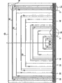
图1描绘了用于等离子体处理装置的喷淋头电极总成10的一个示例性实施方式,其中半导体衬底(例如硅晶圆)在该等离子体处理装置中被处理。该喷淋头电极总成在例如公开号为2005/0133160的共同拥有的美国专利申请中描述过,其内容通过引用并入此处。喷淋头电极总成10包含喷淋头电极,该喷淋头电极包括上电极12、固定到上电极12的支撑构件14和热控制板16。衬底支架18(图1中只显示了它的一部分),其包括下电极和可选的静电夹持电极,被置于该等离子体处理装置的真空处理室中的上电极12下方。经受等离子体处理的衬底20被以机械或静电方式夹持在衬底支架18的上支撑表面22上。
在图示实施方式中,该喷淋头电极的上电极12包括内部电极构件24和可选的外部电极构件30。内部电极构件24优选地是圆柱板(例如,由硅组成的板)并包括暴露于等离子体的底面26和顶面28。内部电极构件的直径可以小于、等于或大于待处理晶圆(例如,直到约8英寸(约200mm),或直到约12英寸(约300mm),如果该板是由硅制成的话)。在一个优选实施方式中,喷淋头电极总成10足够大以处理大衬底,比如具有300mm或更大的直径的半导体晶圆。对于300mm晶圆,上电极12的直径最小为300mm。然而,该喷淋头电极总成的尺寸可以处理其它的晶圆尺寸或具有非圆形外形的衬底。在图示实施方式中,内部电极构件24比衬底20更宽。
为了处理300mm晶圆,提供外部电极构件30以将上电极12的直径从约15英寸扩展到约17英寸。外部电极构件30可以是连续构件(例如,连续多晶硅环)或分段构件(例如,包括2-6个成圆环外形排列的独立段,比如由硅组成的段)。在上电极12包括多个段的外部电极构件30的实施方式中,各段优选地具有边缘,该边缘彼此重叠以保护下面的粘结材料,避免其暴露于等离子体中,并且其中没有气体通道。内部电极构件24优选地包括气体通道32的图案或阵列,其中气体通道32延伸穿过该支撑构件14以将工艺气体注射到位于上电极12和下电极18之间的等离子体反应室中的空间中。可选地,外部电极构件30也包括气体通道的图案或阵列(未示),该气体通道延伸穿过该支撑构件14的支撑环36以将工艺气体注射到位于上电极12和下电极18之间的等离子体反应室中的空间中。
硅是一种用作内部电极构件24和外部电极构件30的等离子体暴露表面的优选材料。两个电极都优选地是由高纯度单晶硅制成的,高纯度单晶硅使等离子体处理过程中衬底的污染最少,并且在等离子体处理过程中平稳磨损,从而使微粒最少。可用于上电极12的等离子体暴露表面的替代材料包括例如SiC或AlN。
在图示实施方式中,支撑构件14包括支撑板34和围绕支撑板34外围延伸的支撑环36。支撑板34包括底面38。在该实施方式中,内部电极构件24是与支撑板34共同延伸的(co-extensive),而外部电极构件30是与周围的支撑环36共同延伸的(co-extensive)。然而,支撑板34可以延伸超出内部电极构件24,从而单一支撑板可以用于支撑内部电极构件24和分段外部电极构件30。内部电极构件24和外部电极构件30通过粘结材料固定于支撑构件14。射频(RF)环形垫片80可以位于内部电极构件24和内部电极构件24的外部外围的支撑板34之间。支撑构件14包含多个孔40,孔40适于接收加固构件42以将支撑构件14固定于热控制板16。支撑板34还包括多个气体通道44,气体通道44延伸穿过支撑板34并与内部电极构件24中的气体通道32流体连通。可选地,支撑环36也包括多个气体通道(未示),该气体通道延伸穿过支撑板36并与外部电极构件30中的可选气体通道(未示)流体连通。
支撑板34和支撑环36优选地是由与等离子体处理室中用来处理半导体衬底的工艺气体化学兼容,并且导电导热的材料制成的。可用于制造支撑构件14的示例性的合适材料包括铝、铝合金、石墨和SiC。支撑板34和支撑环36的优选材料是没有被阳极化的铝合金6061。
可以用合适的导电并导热的弹性体的粘结材料将上电极12固定于支撑板34和支撑环36,该弹性体粘结材料适应热应力,并在上电极12和支撑板34和支撑环36间传递热和电能。使用弹性体将电极总成的各表面粘结起来在例如专利号为6,073,577的共同持有的美国专利中描述过,其内容通过引用并入此处。
在一个实施方式中,该弹性体接缝是弹性胶粘片。该胶粘片可以是任何合适的弹性体材料,比如与真空环境兼容并且在高温(比如200摄氏度)下耐热老化的聚合物材料。该弹性体材料可选地包括导电和/或导热微粒制成的填充剂,或其它形状的填充剂,比如金属丝网、编织或非编织导电纤维。可用于160摄氏度以上的等离子体环境的聚合粘结材料包括聚酰亚胺、聚酮、聚醚酮、聚醚砜、聚对苯二甲酸乙二醇酯、氟乙烯丙烯共聚物、纤维素、三乙酸盐、硅酮和橡胶。
优选地,该胶粘片是将上电极铝(Al)支撑板粘结到单晶硅(Si)喷淋头的导热硅酮粘结剂。优选地,在室温到180摄氏度或更高(例如室温到300摄氏度)的温度范围内,该粘结剂承受至少200%的高剪切应变(shear strain)(例如,200到500%或200到300)。更优选地,该粘结剂承受至少300%的高剪切应变(例如,300到500%)。该粘结剂需要340psi量级的切变应力以达到300%的应变(在室温到180摄氏度或更高温度下)。优选地,该粘结剂需要20到300psi量级的切变应力以达到300%的应变(在室温到180摄氏度或更高温度下)。例如,该粘结剂可需要20-50psi、50-100psi、100-200psi、或200-300psi的切变应力以达到300%的应变(在室温到180摄氏度或更高温度下)。最优选地,该粘结剂可需要20-80psi量级的切变应力以达到200-400%的应变(在室温到180摄氏度或更高温度下)。优选地,该粘结剂呈现线性切变应力/应变曲线,直到至少200%或直到至少300%,在从室温到180摄氏度或从室温到300摄氏度的温度范围内,然而近似线性也是优选的。更优选地,该粘结剂具有在最终故障处的最低可能最大切变应力,例如,在400%应变下(在从室温到180摄氏度或室温到300摄氏度的温度范围内)小于或等于80psi的切变应力。
优选地,当该电极板是直径至少200mm的单晶硅圆片时,该胶粘片呈现线性切变应力/应变曲线,直到至少200%或直到至少300%,在室温到180摄氏度或室温到300摄氏度的温度范围内,来自约5,000个将该电极总成从室温加热到250摄氏度的温度循环之后,20到340psi的切变应力。
当该铝支撑板和硅喷淋头以不同速率热膨胀时,用于将这两个部件粘结起来的该粘结剂耦合这两个部件之间的负载。相反,当该粘结剂是软的(根据一个实施方式,在给定应变下有低切变应力)时,这两个部件不会引起应力或隔板偏转到彼此中。优选地,该支撑板和喷淋头具有在这两个配合表面的非粘结区域间有空隙。隔板偏转可能使得在两个部件的热膨胀过程中,该支撑板表面的非粘结区域与该喷淋头表面的非粘结区域接触并摩擦。这样的摩擦可能从一个或两个表面上磨掉微粒。而且当隔板偏转存在于该上电极总成中时,在该铝支撑板与该热控制板配合的地方可能出现更高的局部接触负载。这可能导致该支撑板和该热控制板之间的擦伤,在该系统内产生微粒。因此,当该粘结剂是软的时,由于没有或很少隔板偏转以及在该支撑板和热控制板之间没有或很少来自由于热膨胀系数不匹配而带来的部件变形带来的擦伤,所以产生更少的微粒污染物。
该胶粘片可以是仅用高分子量二甲基硅酮和可选的填充剂配制的,或者它可以是围绕玻璃纤维筛(纱布)或金属筛成长的或者与玻璃微珠和/或玻璃或其它材料的纳米珠混合成的,以适应各种应用的要求。优选地,该胶粘片是用围绕Al2O3微珠成母体的高分子量二甲基硅酮配制的。胶粘片的组合层可以被制造或叠层,其具有不同的物理性质。在一个优选实施方式中,该胶粘片的共面区域可以被离散地配制为具有不同的物理性质。物理性质的例子是导热性、弹性、拉伸和切变强度、厚度、热膨胀系数、耐化学性、微粒腐蚀和工作温度范围。
例如,填充用弹性体材料可以经受等离子体腐蚀并且有可能在等离子体处理过程中释放导电填充剂微粒。在等离子体处理过程中,离子或基团可能移动到气体通道32中,导致围绕该孔的接缝交界处的该填充用弹性体材料的腐蚀。例如,在蚀刻工艺过程中,源自被等离子体腐蚀的弹性体材料的铝合金填充剂微粒可能沉积在晶圆上而产生缺陷。在用于减少导电填充剂微粒的释放的一个实施方式中,该胶粘片的共面区域可以被离散地配置有不同的填充剂微粒密度。例如,暴露于通过气体通道32迁移过来的离子或基团的接缝交界处的该胶粘片的区域可以不被填充(没有填充剂微粒),而不暴露于该离子或基团的该胶粘片的共面区域可以包括填充剂微粒。
优选地,该弹性胶粘片的该高纯度弹性体材料是基于联苯二甲基硅酮共聚物的热固化导热硅酮。优选的弹性胶粘片是从导热室温未硫化的硅酮片配制的,该硅酮片是可以从NUSIL TECHNOLOGY公司得到的商品HCR-9800-30。优选地,该硅酮胶粘片产品使用Al2O3填充剂,并被配制为是热固化的,也就是说,优选地,该胶粘片不需要单独的活化剂施加来启动交联(cross-linking)反应。优选地,该胶粘片被配置为具有合适的热活化成分以在预定固化温度下执行该交联反应,例如,该热活化交联剂可以是过氧化物。这样配制的胶粘片可以从NUSIL TECHNOLOGY公司获得。
在该弹性体是导电弹性体的情况下,该导电填充剂材料可以包含导电材料的微粒。可用于等离子体反应室的对杂质敏感的环境的潜在导电材料是镀镍碳粉、镍粉、碳纳米管、石墨烯、石墨及其结合。
在该弹性体是导热弹性体的情况下,该导热填充剂金属可以包含导热金属或金属合金微粒。可用于等离子体反应室的对杂质敏感的环境中的一种优选金属是铝合金、氧化铝(Al2O3)或氮化硼(BN)。优选地,该弹性胶粘片具有低强度,可以承受高剪切应变并具有高导热率。优选地,热传导率在0.5W/mK,更优选地在0.8W/mK,最优选地至少1.0W/mK。在弹性胶粘片中比在液体或浆糊弹性体粘结材料中能够实现导热和/或导电微粒的更均匀分布。
为了保持在最终形成的接缝的弹性极限内,可以使用合适的粘结厚度。也就是说太薄的胶粘片接缝在热循环过程中可能撕裂而太厚的胶粘片接缝会减少其连接的部件间的热传导率。不是一定要使用导电和/或导热的弹性体,因为由于该电极和该支承构件之间的电容耦合,足够的RF电力可以通过该弹性体接缝的薄的区域提供给该电极。
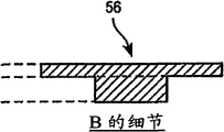
图1显示了多个缺口48位于支撑板34中的实施方式,其中支撑板34具有位于其中的胶粘片52的扁平环以粘结内部电极构件28和支撑板38的配合表面。图1的实施方式显示了缺口54,缺口54具有更大的深度以接收扁平环胶粘片56。这个实施方式还显示,在内部电极构件24和内部电极构件24的外围附近的支撑板34之间有RF垫圈80。在图1的实施方式中,外部环电极30可以通过支撑环58的缺口中的胶粘片60的单一扁平环粘结于支撑环36。
该电极和支承构件的配合表面可以是平面的或非平面的。例如,一个吻合表面可以是平面的,而另一个可以包括用于接收该胶粘片粘结材料的缺口。例如,这样的缺口可以保护该胶粘片免于暴露于等离子体。替代地,该配合表面的外形可以提供连锁和/或自我对准布置。为了提高该弹性体粘结材料的粘结性,该配合表面优选地涂覆有合适的底胶。当该粘结材料是从上述NUSILTECHNOLOGY HCR-9800-30材料配制而成时,该底胶可以是NUSIL TECHNOLOGY制造的商品名为SP-120或SP-270的硅酮底胶。优选地,这样的底胶被用于该配合表面,并在将该胶粘片放置在待粘结表面位置之前被干燥。
该底胶可以作为薄涂层通过任何合适技术施加,比如擦拭、刷、喷淋,优选地在该喷淋头总成元件的离散的粘结表面上以形成后来施加的粘结材料的粘结点。如果该底胶包含溶剂,通过擦拭施加该底胶可以通过清洁该表面而增强粘结。当在空气中在室温下固化时,含硅氧烷的底胶与空气反应并产生硅粘结点。这样的底胶提供粘结点的量的可视指示,因为有过量底胶的位置显得满是粉末。
该胶粘片优选地在用于处理的转移片之间。优选地,该转移片是由DUPONT制造的TEFLON。转移片优选地阻止例如未固化的胶粘片的变形和损害。通过除去一个转移片并将该胶粘片的暴露表面应用到第一配合表面、除去另一个转移片并将第二配合表面应用到该胶粘片的另一个暴露表面,而将该胶粘片应用到到配合表面或底涂过的配合表面。该胶粘片表面可以是粘的(tacky)并且优选地,可以使用工具以精确地除去转移片而将该胶粘片放在配合表面上。更优选地,该配合表面上的该胶粘片可以被放在真空下以吸出该粘结剂下方的任何空隙或空穴并施加临时固定载荷(seating load),比如通过真空装袋。
在该胶粘片粘结材料被施加到该表面中的至少一个之后,该部件可以被组合从而各表面在压缩下、在静态重量下或通过真空袋内的大气压而被压在一起。因此该弹性体是胶粘片形式的,所以不是一定要施加初始轻微压力(比如手的压力)以使该弹性体在整个待形成的接缝上展开。然而,轻微压力(比如手的压力)或真空袋内的轻的大气压负载是需要的,以使该粘结剂固定(seat)于该配合表面。在大约五分钟或更少的固定载荷之后,优选地,除去该粘结剂上的所有载荷。该固化应当优选地在没有任何显著的静态重量或真空袋负载的情况下被执行。该粘结可以在较高温度下在大气压或保护气体环境下固化。该总成可以被放于对流烘箱中并被加热以活化固化该粘结的交联处理。例如,热固化的粘结材料被在110摄氏度到122摄氏度之间的初级固化温度下(例如,116摄氏度)处理10到20分钟(例如15分钟)。在成功检查该总成之后,该粘结材料被在140摄氏度和160摄氏度之间的次级固化温度(例如,150摄氏度)下处理1.5到2.5小时(例如,2小时)。替代地,只有该次级固化被施加2.5到3.5小时(例如,3.5小时),跳过初级固化。
优选地,该胶粘片保持其几何形状从而在粘结和固化过程中该胶粘片不凸起或流动。然而,固化过程中该胶粘片的体积变化可以达到5%的体积收缩。优选地,该胶粘片在固化过程中经历不多于2到3%的体积收缩。
在等离子体处理过程中,该弹性体粘结电极总成能够保持高工作温度、大功率密度和长射频小时。而且,在半导体晶圆的等离子体处理过程中,使用粘结剂弹性体材料作为连接电极总成的机构相对非胶粘片有额外的优点。
具有残留的未使用的底胶的元件的区域(非粘结区域)可能是污染源。例如,使用硅氧烷底胶(例如,RHODIA SILICONES VI-SILV06C)已经确定具有引入污染物(包括钛)水平的可能。钛污染物有可能与硅衬底反应,在蚀刻处理过程中在该衬底的不想要的区域中形成硅化钛。
通过将该底胶选择性施加在该喷淋头总成上稍后会施加胶粘片粘结材料的区域,而不是用该底胶涂覆所有表面,胶粘片允许减少源自该底胶材料的污染物。图2是内部电极构件24的俯视图,内部电极构件24包括多个延伸穿过底部等离子体暴露表面26的气体通道32。在此实施方式中,该胶粘片弹性体材料作为环形区图案46被施加到包含气体通道32的区域之间。然而,在施加该弹性体材料之前,可以以对应于该弹性体材料的同样的环形区图案施加底胶。
尽管图中显示该胶粘片是施加在环形区的然而施加胶粘片的图案不受限制而且可以以其它图案(比如不是环形的区域)施加。胶粘片可以被以任何期望的图案切割以及从该转移片除去的部分以允许该胶粘片的离散部分向相连接的部件的转移。
该底胶可以以预定的粘结区域图案(被非粘结区域围绕)被施加到内部电极构件24的顶面28。在一个实施例中,通过围绕其中心点C旋转内部电极构件24,并通过在单一位置或相对于该中心点C的多个半径位置接触分发器的一个或多个出口,每次生成一个或多个环形区,而用该分发器(例如,神经末梢分发器)按图案46施加该底胶。在另一个实施例中,该环形区图案(或任何期望图案)可以通过用具有预定图案的开口的掩模覆盖内部电极构件24的顶面28而施加。然而,该底胶可以以任何适当的预定图案(例如,多个离散区域、半径和/或间断的环形区)施加,只要该底胶只施加到该胶粘片弹性体材料下的区域。该底胶还可以通过该掩模的开口通过擦拭、刷、喷淋施加。上面描述的两种方法还可以用于将底胶施加到支撑板34的底面38。在只将该底胶施加到该胶粘片弹性体材料下方的选定区域46中时,与该底胶的施加有关的污染物可以显著减少。
掩模材料的例子可以包括(聚酰亚胺基材料)、 (聚酯基材料)或
 (氟聚合物树脂),都可以从DU PONT得到。
该胶粘片比液体、凝胶和浆糊状粘结剂好的另一个优点是流量控制或流量消除。例如,如图3A所示,当待连接的喷淋头总成元件包含气体通道32/44时,液体或浆糊状的未固化弹性体材料50的流动在该弹性体被固化之前在该元件被压在一起时必须被控制。当未固化的浆糊50被施加到两个元件之间并被按压时,难以控制该未固化的弹性体材料的流动。如图3B所示,未固化弹性体材料50的无控制流动导致气体通道32/44的阻塞或堵塞。结果是,需要额外的清洁或机械加工来清洁被阻塞或堵塞的气体通道32/44。该胶粘片弹性体材料可以避免这样的问题,因为该胶粘片52可以以比图4A所示的液体或浆糊弹性体材料更细微的容差被放置在待连接的喷淋头总成元件之间。该胶粘片可被配置为呈现出良好的体积控制从而不会渗漏或流入不期望的区域。同样地,胶粘片弹性体材料52可以比液体、浆糊或凝胶更靠近气体通道32/44而没有阻塞或堵塞气体通道32/44的危险。
当上电极12和支撑构件14是由具有不同热膨胀系数的材料组成的时,该弹性体材料的厚度可以被改变以适应热膨胀的差异。例如,上电极12可以是硅而支撑构件14可以是金属(例如,铝、不锈钢、铜、钼或其合金)。然而,如果具有更大的热膨胀系数差异的两个元件被粘结起来(即,铝和硅),在温度固化过程中或该电极操作过程中加热时,在该弹性体粘结材料中会由于不同的热膨胀率而产生不均匀的切变应力。例如,如果圆形的铝支撑构件14被同心地粘结于圆形硅上电极12的话,支撑构件14和上电极12的中心附近的弹性体粘结材料中的切变应力在更高的处理温度下是最小的。然而,铝支撑构件14的外部部分会比硅上电极12的外部部分经受更大量的热膨胀。因此,当这两个材料粘结起来时,在支撑构件14或上电极12的外部圆周边缘中(在那里热膨胀的差异是最大的)出现最大的切变应力。
片的形式的粘结剂可以提供卓越的粘结厚度控制以精确控制粘结表面在很大面积上的平行度从而不需要插入物或垫片来控制粘结厚度或平行度。图4A显示了粘结于气体通道44之间的支撑板34的底面中的缺口48的胶粘片52的一个实施方式。图4B显示了粘结于气体通道32/44之间的支撑板34的底面38和上电极24的顶面28的胶粘片52。
片的形式允许卓越的体积控制以限制或阻止粘结剂泄漏到不期望的区域。胶粘片的应用免除了对用于施加液体或浆糊粘结剂的精确的分发设备的需要。因此消除了自动化和/或人工分发过程的供料速度问题,以及相关的粘结剂分发小珠的干燥、颈缩(necking)或成球(globing)问题。该胶粘片有更均匀的导热填充剂的悬浮、预期更好的货架寿命,并可以提供更高效而可靠的制造处理过程。
可以设计预成形(pre-form)胶粘片的形状以符合不规则形状的平面特征,并可以被优化以最大化与配合部件的表面接触面积。例如,在图3A中,液体或粘结浆糊50的小珠沿着缺口48中的横截面显示的小珠50的弯曲表面接触支撑板34。小珠50和支撑板38的配合表面之间的接触面积比小珠50更窄,并且难以控制粘结的均匀性和可再现性。在图3B中,当电极24被配合到支撑板34时,液体或浆糊粘结剂小珠50和支撑板和电极38/28的配合表面之间的接触被限制,并且难以控制,从而该接触面积会比小珠50的直径更小,为了实现支撑板34和电极24之间合适的粘结强度和导热和/或导电率所需的接触面积,需要过量的液体或浆糊粘结剂。
在图4A中,弹性胶粘片52沿着平行于支撑板表面的缺口48中横截面显示的胶粘片的预定表面精确地接触支撑板34。胶粘片52和支撑板34和电极24的配合表面38/28之间的接触面积提供了对于图4B中所示的弹性体粘结剂的体积的最大接触面积比例。胶粘片52的更大的接触面积允许在粘结时使用更少的弹性胶粘片52来达到支撑板34和电极24之间合适的导热和/或导电率、粘结强度和粘结弹性。
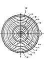
优选地,该胶粘片可以被切割为预成形形状,例如通过激光、水力喷射、冲模切割、绘图切割及其他切割方法。该胶粘片还可以被浇铸成预成形形状,例如通过浇铸,比如带式浇铸、滚筒或喷墨印刷。图5A-C显示了胶粘片100被切割为扁平环52的一个优选实施方式。图5A显示了胶粘片100和有各种内径和外径的扁平环52(即,该扁平环可以有各种平面宽度)的平面图。图5B显示了图5A中的胶粘片实施方式的侧视图。图5C显示了图5A中的胶粘片实施方式的区域“A”的细节视图,描绘了从片100切割出的有很窄的平面宽度和很大直径的胶粘片环。例如,胶粘片100的厚度可以是0.012英寸(305μm),且扁平环52的内径和外径可以是(以英寸计):(0.195,0.464),(0.854,1.183),(1.573,1.902),(2.725,3.625),(4.449,4.778),(5.168,5.497),(6.320,7.220),(8.043,8.372),(9.196,10.096),(10.919,11.248),(11.638,11.724)和(11.913,12.000)。
优选地,该胶粘片和胶粘片52的扁平环是作为TEFLON(未示)的转移片之间的叠层被切割、处理和转移的。图6显示了被置于支撑板34的配合表面38中的缺口48上方的胶粘片52的扁平环的横截面。这样的缺口48是跑道凹槽形式的。尽管不是优选的,胶粘片的扁平环可以具有凸起部(elevation jog)。图6显示扁平环胶粘片56具有凸起部从而该扁平环沿着它的平面宽度有不断改变的厚度。扁平环胶粘片56匹配支撑板34中的跑道凹槽54。图7显示了图6中的胶粘片环56中的凸起部的细节视图“B”,其中胶粘片环在该环的中心更厚。这样的凸起部可以是例如通过层压(laminating)具有不同径向宽度和/或不同轴向高度(厚度)的胶粘片的扁平环制成的。图8显示了为了接收胶粘片环56而在支撑板34中形成的缺口54的细节视图“D”。
图9显示了图6中显示的支撑板34(未反转的)的细节视图“E”。配合表面38中的缺口48可以被定位以精确控制粘结和非粘结区域。该非粘结区域可以是配合表面38的表面面积的1%到95%。例如,该非粘结区域可以是配合表面38的表面面积的1-5%、5-10%、10-15%、15-20%、20-30%、30-40%、40-50%、50-60%、60-70%、70-80%、80-90%或90-95%。气体通道44在非粘结区域中而该胶粘片粘结该粘结区域。胶粘片的边缘(例如,扁平环52的内径或外径)和表面38中的气体通道44的开口之间的距离可以被精确控制以优化粘结性质,并且如同前面提到的,消除了非片状弹性体粘结剂的泄漏或膨胀堵塞气体通道44的危险。优选地,该胶粘片在固化前、固化过程中和固化后基本上保持它的原始尺寸并且保持同样的形状而不会缩小或缩小很少,例如,固化后有2-3%的体积缩小。
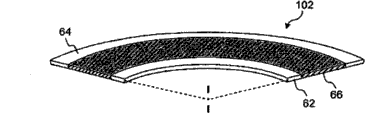
作为优选实施方式,该胶粘片可以是在厚度方向(叠层的)或平面方向(共平面的)上有一个或多个不同物理性质的各种平面宽度的扁平环的组合层。图10显示了具有不同的共平面物理性质的扁平环胶粘片102的一部分。例如,内部部分62和外部部分64可以是用于低微粒污染物释放的未填充的硅酮弹性胶粘片,而中间部分66可以包含用于热传导的Al2O3微粒。
图11显示了胶粘片104的一个实施方式。胶粘片104可以是各种宽度的具有凸起部68(小台阶)的多个扁平圆形或半圆形环。表面70和72可粘结于电极配合表面中的缺口(未示,但是类似于支撑构件14中的缺口48、54和58)或表面70可粘结于没有缺口的电极配合表面,比如内部电极配合表面28和/或外部电极环30的配合表面。表面74和76可粘结于类似于缺口48、54和58的支撑构件14的配合表面中的缺口或表面76可粘结于没有缺口的支撑板和/或支撑环配合表面(未示)。
例如,该胶粘片可以被排列为各种宽度和厚度的点、三角形、行列、及其他几何形状的均匀或非均匀图案而不受限制。图12显示了圆锥体106、方形条108、三角形110、圆点112和具有凸起部114的圆点式的胶粘片。该胶粘片可以是多个这样的几何形状以粘结支撑构件14和电极12的配合表面上的粘结区域。然而,在另一个实施方式中该胶粘片可以是具有“蜘蛛网”几何形状的单一一片以精确匹配粘结区域同时为气体通道32/44留出非粘结区域。图12显示了用于粘结例如配合表面28和38的单片116的实施方式的平面图。相应地,胶粘片116中的空隙78对应于非粘结区域。在此实施方式中,这样的非粘结区域会对应于配合表面面积的90%以上。
在固化以前,该胶粘片优选地具有物理上稳定的性质。固化以前的胶粘片是具有尺寸稳定性的未硫化的、未交联的成分。该未固化的胶粘片可以是可延展的。如同提到过的,优选使用转移片来处理未固化的胶粘片以防止该胶粘片在固化前变形。在加热时,交联剂(比如过氧化物填充剂)优选地以与未固化的胶粘片总体相同的形状固化该胶粘片。在固化以后,该胶粘片在机械力被除去以后回到相同的形状。更大的接触面积控制增加了粘结的部件之间的导热和/或导电率。固化的胶粘片还保持可与固化的凝胶弹性体相比在高容量的填充剂微粒下的弹性,以及比固化的液体和浆糊弹性体在高容量填充剂微粒下的更大的弹性。对于给定容量的弹性体粘结剂,通过在该弹性胶粘片中使用高容量填充剂微粒,在各粘结部件之间可以实现更大的导热和/或导电率而不会牺牲粘结强度或弹性。
优选地,预成形的形状被安装到该配合总成的捕获腔(captivating cavities)48中。安装可以通过比如人工执行、用安装工具人工执行或用自动化机械执行等方法执行。该胶粘片可以被配制为具有有限或无限的工作时间,然后当方便固化时被热固化。
如图4A和4B所示,支撑构件34以这种方式被连接于内部电极24,即该内部电极24的第一气体通道32和支撑构件34的第二气体通道44流体联通。为了增强粘结性,底胶46也可以被以与施加到内部电极构件24的顶面28的相同的预定图案被施加到支撑构件34的底面38。在替代实施方式中,支撑构件34或内部电极构件24可包含增压室(plenums)从而以期望的气体分配图案分配一个或多个气体供应。在另一个实施方式中,气体通道32可以与一个或多个气体通道44流体连通。
在一个优选实施方式中,该胶粘片将电极28的顶面粘结于支撑板38的底面,使得在非粘结区域中之间有51到381μm(0.002到0.015英寸)的空隙。例如,该支撑板底面和/或该电极顶面上的缺口48的深度优选地是102到508μm(0.004到0.020英寸),例如100到200μm或200到500μm。更优选地,该缺口48的深度是178μm(0.007英寸)。然而,该支撑板底面和电极顶面可以通过该胶粘片粘结而无需缺口。更优选地,该胶粘片将该支撑板底面平行于该电极顶面粘结,其中两个配合表面之间的距离在小于+/-25μm(0.001英寸)之间变化。
该支撑板34被通过合适的加固构件附着于热控制板16,例如,在共同持有的美国专利申请公开号2007/006829中所描述的,其内容皆由引用而纳入此处。支撑构件34容纳多个适于接收加固构件42的孔40以将支撑构件34附着于热控制板16。
实施例
胶粘片的非限制性实施例被像上面描述的那样配制、热固化和测试。试验样品是由胶粘片组成的以模拟胶粘片在配合表面之间的粘结中的性能,然而应当注意,电极和支撑构件之间的实际粘结的试验结果没有在这里显示。剪切试验是在室温下和在较高温度下(例如,在180摄氏度下)执行的。高温疲劳测试是在例如180摄氏度下执行的。图14显示了在室温下实施例1胶粘片的剪切试验结果。实施例1显示了一个近似线性的应力应变曲线,有超过300%的剪切应变以及在高剪切应变下的低切变应力。用这样的软的胶粘片制成的粘结适于适应高剪切应变而没有耦合力引起的粘结的电极和支承板之间的隔膜形成(diaphraming)。
图15和17显示了在180摄氏度下实施例2胶粘片的剪切试验结果。实施例2经历了近似线性的线性应力应变曲线,在180摄氏度下有超过300%的剪切应变和高应变下的低强度。这样的软胶粘片粘结适于适应高剪切应变而没有粘结的电极和支撑板之间的隔膜形成(diaphraming)。
图16显示了在180摄氏度下实施例3胶粘片的疲劳试验结果。该疲劳试验被执行超过36,000个循环(cycles)(显示了约35,000个)。尽管只测试了胶粘片的样品,然而每个循环模拟了一次热循环,其中在等离子体处理过程中由于该支撑板和电极的材料的热膨胀系数的差异,支撑板扩展的量不同于电极的扩展的量。图17显示了在超过36,000个循环的疲劳试验后在180摄氏度下实施例3胶粘片的剪切试验结果。实施例3呈现了近似线性的应力应变曲线,在180摄氏度下有超过300%的剪切应变以及在高应变下的低强度。例如,实施例3呈现了接近线性的应力应变曲线,剪切应变范围为约0%到约450%。这样的软胶粘片粘结适于适应高剪切应变而即便在36,000个温度循环后仍没有粘结的电极和支撑板之间的隔膜形成(diaphraming)。
尽管本发明是参考其具体实施方式进行详细描述的,然而,对本领域的技术人员来说,显然,可以在不悖离所附权利要求的范围的基础上,对本发明作出变更和修改。
Claims (25)
1.一种用于在等离子体处理装置生成等离子体的组合喷淋头电极总成,包含:
包含顶面和底面的支撑板,在该顶面和该底面之间有第一气体通道,该底面具有粘结和非粘结区域,该第一气体通道在非粘结区域中有出口以向该等离子体处理装置的内部供应工艺气体;
具有顶面、等离子体暴露底面和在该顶面和该底面之间延伸并与该第一气体通道流体连通的第二气体通道的电极板,其中该第二气体通道在该电极板的顶面的非粘结区域中有进口;以及
在每个粘结区域、位于配合表面之间的弹性胶粘片接缝,该胶粘接缝允许在温度周期变化过程中由于该电极板和该支撑板中热膨胀系数的不匹配而产生的该电极板相对于该支撑板的横向移动。
2.根据权利要求1所述的组合喷淋头电极总成,其中
该支撑板包含内部支撑板和外部支撑环,该外部支撑环围绕该内部支撑板,其中该第一气体通道在该内部支撑板中并可选地在该外部支撑环中,
该电极板包含粘结于该内部支撑板的内部喷淋头电极和粘结于该外部支撑环的外部环形电极,其中该第二气体通道在该内部喷淋头电极中并可选地在该外部环形电极中。
3.根据权利要求2所述的组合喷淋头电极总成,其中(a)该支撑板的配合表面平行于该喷淋头电极的配合表面和/或(b)该 电极是单晶硅、多晶硅、石墨或碳化硅的;以及该支撑构件是铝、石墨或碳化硅的。
4.根据权利要求1所述的组合喷淋头电极总成,其中该弹性胶粘片接缝包含导热硅酮胶粘片。
5.根据权利要求4所述的组合喷淋头电极总成,其中该弹性胶粘片接缝在室温到200摄氏度的温度范围内从约20到340psi的切变应力在横向方向上可以弹性变形到至少200%的剪切应变。
6.根据权利要求5所述的组合喷淋头电极总成,其中该弹性胶粘片接缝从约20到80psi的切变应力在横向方向上可以弹性形变到至少300%的剪切应变。
7.根据权利要求5所述的组合喷淋头电极总成,其中该电极板是直径为至少200mm的单晶硅圆盘而该弹性胶粘片接缝是在5000个将该喷淋头电极总成的温度从室温加热到250摄氏度的温度循环之后,在室温到300摄氏度的温度范围内,从约20到340psi的切变应力在横向方向上可以弹性形变到至少200%的剪切应变。
8.根据权利要求4所述的组合喷淋头电极总成,其中该导热硅酮胶粘片包含两个或多个有不同物理性质的叠层和/或该导热硅酮胶粘片包含两个或多个有不同物理性质的共平面部分。
9.根据权利要求4所述的组合喷淋头电极总成,其中该导热硅酮胶粘片的一个部分具有0.5W/mK到0.8W/mK的导热率,该导热硅酮胶粘片的至少一个部分有0.8W/mK到1W/mK的导热 率和/或该导热硅酮胶粘片的至少一个部分有超过1W/mK的导热率。
10.根据权利要求4所述的组合喷淋头电极总成,其中(a)该弹性胶粘片接缝进一步包含在该支撑构件和/或该电极背部的一个或多个配合表面上的底胶;和/或(b)该导热硅酮胶粘片包含均匀分布的导热填充剂。
11.根据权利要求10所述的组合喷淋头电极总成,其中(a)该导热填充剂是氮化硼(BN)、氧化铝(Al2O3)、硅、碳化硅及其结合之一和/或(b)该导热硅酮胶粘片是(i)高分子量二甲基硅酮和该导热填充剂,(ii)高分子量二甲基硅酮和围绕玻璃纤维筛成长的导热填充剂,(iii)高分子量二甲基硅酮和围绕金属筛成长的导热填充剂或(iv)高分子量二甲基硅酮和与玻璃微珠或纳米珠混合的导热填充剂制成的。
12.根据权利要求1所述的组合喷淋头电极总成,其中一该配合表面之间的空隙距离的变化小于±0.001英寸。
13.根据权利要求1所述的组合喷淋头电极总成,其中(a)该弹性胶粘片接缝包含被浇铸或被轧制成预成形形状的弹性胶粘片;(b)该弹性胶粘片接缝包含冲模切割的预成形形状的弹性胶粘片;(c)该弹性胶粘片接缝包含激光切割、绘图切割和/或水力喷射切割成预成形形状的弹性胶粘片;和/或(d)该配合表面之一包含缺口。
14.根据权利要求13所述的组合喷淋头电极总成,其中(a)该缺口的深度在100到200μm范围内;(b)在缺口的深度在200到500μm范围内;(c)该缺口包含凸起部,该凸起部的尺寸与该胶粘片的尺寸相匹配;(d)该胶粘片将该电极的顶面粘结 到该支撑构件的底面,其中该电极的顶面和该支撑构件的底面之间的间隔为50到400微米;(e)该胶粘片接缝包含单片形式的硅酮胶粘片;(f)该胶粘片接缝包含一个或多个扁平环、具有凸起部的扁平环、圆柱体、扁平或柱状多角形、块状或其结合的形式的硅酮胶粘片;和/或(g)该弹性胶粘片接缝包含热固化粘结剂。
15.一种用于等离子体处理装置的用于连接组合喷淋头电极总成的各元件的方法,包含:
以预定图案将未固化弹性胶粘片的第一表面施加到粘结区域的预定图案的支撑构件的底面,该粘结区域不包括要保持非粘结的区域,该支撑构件具有顶面和在该顶面和该底面之间延伸并在非粘结区域中有出口的多个第一气体通道;
以粘结区域的预定图案将电极的顶面施加到未固化弹性胶粘片的第二表面,该电极具有等离子体暴露底面和多个在该电极的该顶面和该底面之间延伸的第二气体通道,其中该第二气体通道在该电极的该顶面的非粘结区域中有进口;以及
将该电极的该顶面粘结到该支撑构件的该底面,该弹性胶粘片在该电极的该顶面与该支撑构件的该底面之间,其中该第二气体通道与该第一气体通道流体连通。
16.根据权利要求15所述的用于连接组合喷淋头电极总成的各元件的方法,进一步包括:
以预定图案向该支撑构件的底面施加底胶;以及
以预定图案向该电极的该顶面施加底胶。
17.根据权利要求15所述的用于连接组合喷淋头电极总成的各元件的方法,其中向该电极的该顶面施加底胶包含:
围绕其中心点旋转该电极并通过使分发器的出口与该旋转电极在相对于该中心点的多个径向位置接触而用该分发器沉积该底胶的环形区;或
用具有预定图案的开口的掩模覆盖该顶面并在该顶面的无屏蔽区域上涂覆该底胶。
18.根据权利要求17所述的用于连接组合喷淋头电极总成的各元件的方法,其中该掩模中的该预定图案是多个半环形区。
19.根据权利要求16所述的用于连接组合喷淋头电极总成的各元件的方法,其中向该支撑构件的该底面施加底胶包括:
围绕其中心点旋转该支撑构件并通过使该分发器的出口与该旋转支撑构件在相对于该中心点的多个径向位置接触而用该分发器沉积该底胶的环形区;或
用具有预定图案的开口的掩模覆盖该底面并在该底面的无屏蔽区域上涂覆该底胶。
20.根据权利要求15所述的用于连接组合喷淋头电极总成的各元件的方法,其中
(a)施加该弹性胶粘片的该第一表面包含使用机械切割、冲模切割、激光切割、水力喷射切割、等离子切割、绘图切割及其组合将该弹性胶粘片的粘结材料预切割为预定图案;
(b)该电极的顶面和/或该支撑构件的底面包含在该预定图案的至少一部分上方的通道;
(c)该弹性胶粘片是填充的、未固化的弹性硅酮片;和/或
(d)该填充的、未固化的弹性硅酮片是用铝、氧化铝、硅、碳化硅、氮化硼或其合金制成的导热颗粒。
21.根据权利要求15所述的用于连接组合喷淋头电极总成的各元件的方法,其中
(a)粘结进一步包括通过在压缩下、在静态重量下或可选地通过真空袋内的气压将该电极的顶面和该支撑构件的底面压在一起而固定该胶粘片,其中该弹性胶粘片是热固化的;
(b)当该静态重量或可选的真空袋内的气压被除去时,在固定后,加热该组合喷淋头电极总成以固化该粘结材料;
(c)该电极是硅、石墨或碳化硅的;以及该支撑构件是铝、石墨或碳化硅的;
(d)施加该弹性胶粘片的该第一表面包含在向该支撑构件的底面施加该第一表面之前从该第一表面除去转移片;
(e)施加该电极的顶面包含在向该胶粘片的该第二表面施加该电极的顶面之前,从该弹性胶粘片的该第二表面除去转移片;
(f)施加弹性胶粘片的该第一表面包含在向该支撑构件的底面施加该第一表面以后施加真空以除去其间的空隙;
(g)施加该电极的顶面包含在向该弹性胶粘片的该第二表面施加该电极的顶面之后施加真空以除去其间的空隙;和/或
(h)该电极包含内部喷淋头电极和外部环形电极而该支撑构件包含内部支撑板和外部支撑环。
22.一种在等离子体处理装置中处理半导体衬底的方法,该方法包括:
将该衬底放入等离子体处理装置的反应室的衬底支座上;
使用权利要求1的该组合喷淋头电极总成将工艺气体引入该反应室;
在该反应室中在该组合喷淋头电极总成和该衬底之间从该工艺气体生成等离子体;
用该等离子体处理该衬底。
23.根据权利要求22的方法,其中该处理包含蚀刻该衬底。
24.一种用于等离子体处理装置的组合喷淋头电极总成,包含:
支撑构件,该支撑构件包括具有待粘结区域、排除保持不被粘结的区域的底面以及在该底面和该支撑构件的顶面之间延伸的多个第一气体通道,其中该第一气体通道在保持不被粘结的区域中有出口,以将工艺气体供应到等离子体处理装置的内部;
在该等离子体处理装置中产生等离子体的电极,该电极具有有待粘结区域的顶面和与该第一气体通道流体连通的多个第二气体通道,该第二气体通道在保持不被粘结的区域中有进口,该第二气体通道从该顶面到该电极的等离子体暴露底面延伸穿过该电极;以及
未固化弹性胶粘片,其要被固化在每个待粘结区域的配合表面之间的接缝中以允许在温度周期变化过程中由于该支撑构件和该电极的热膨胀系数的不匹配而产生的该电极相对于该支撑构件在横向方向上的移动,
其中弹性胶粘片是填充的、热固化的、未硫化的弹性硅酮片。
25.根据权利要求24的组合喷淋头电极总成,其中该未固化的弹性胶粘片是用过氧化物作为热活化成分以执行交联反应而配 制的,该弹性胶粘片在固化过程中的体积收缩是3-5%,或小于3%。
Applications Claiming Priority (3)
| Application Number | Priority Date | Filing Date | Title |
|---|---|---|---|
| US815207P | 2007-12-19 | 2007-12-19 | |
| US61/008,152 | 2007-12-19 | ||
| PCT/US2008/013782 WO2009085163A1 (en) | 2007-12-19 | 2008-12-17 | A composite showerhead electrode assembly for a plasma processing apparatus |
Publications (2)
| Publication Number | Publication Date |
|---|---|
| CN101903979A CN101903979A (zh) | 2010-12-01 |
| CN101903979B true CN101903979B (zh) | 2012-02-01 |
Family
ID=40789176
Family Applications (1)
| Application Number | Title | Priority Date | Filing Date |
|---|---|---|---|
| CN200880123061XA Active CN101903979B (zh) | 2007-12-19 | 2008-12-17 | 组合喷淋头电极总成、连接其各部件的方法及衬底处理方法 |
Country Status (8)
| Country | Link |
|---|---|
| US (2) | US8418649B2 (zh) |
| JP (1) | JP5265700B2 (zh) |
| KR (1) | KR101553422B1 (zh) |
| CN (1) | CN101903979B (zh) |
| MY (1) | MY166000A (zh) |
| SG (2) | SG10201407723PA (zh) |
| TW (1) | TWI507093B (zh) |
| WO (1) | WO2009085163A1 (zh) |
Families Citing this family (45)
| Publication number | Priority date | Publication date | Assignee | Title |
|---|---|---|---|---|
| US7645341B2 (en) * | 2003-12-23 | 2010-01-12 | Lam Research Corporation | Showerhead electrode assembly for plasma processing apparatuses |
| US8702866B2 (en) | 2006-12-18 | 2014-04-22 | Lam Research Corporation | Showerhead electrode assembly with gas flow modification for extended electrode life |
| US8069817B2 (en) * | 2007-03-30 | 2011-12-06 | Lam Research Corporation | Showerhead electrodes and showerhead electrode assemblies having low-particle performance for semiconductor material processing apparatuses |
| MY166000A (en) * | 2007-12-19 | 2018-05-21 | Lam Res Corp | A composite showerhead electrode assembly for a plasma processing apparatus |
| WO2009078923A2 (en) | 2007-12-19 | 2009-06-25 | Lam Research Corporation | Film adhesive for semiconductor vacuum processing apparatus |
| US8161906B2 (en) * | 2008-07-07 | 2012-04-24 | Lam Research Corporation | Clamped showerhead electrode assembly |
| US8206506B2 (en) * | 2008-07-07 | 2012-06-26 | Lam Research Corporation | Showerhead electrode |
| US8221582B2 (en) * | 2008-07-07 | 2012-07-17 | Lam Research Corporation | Clamped monolithic showerhead electrode |
| US8147648B2 (en) * | 2008-08-15 | 2012-04-03 | Lam Research Corporation | Composite showerhead electrode assembly for a plasma processing apparatus |
| US8869741B2 (en) * | 2008-12-19 | 2014-10-28 | Lam Research Corporation | Methods and apparatus for dual confinement and ultra-high pressure in an adjustable gap plasma chamber |
| US8402918B2 (en) * | 2009-04-07 | 2013-03-26 | Lam Research Corporation | Showerhead electrode with centering feature |
| US8272346B2 (en) | 2009-04-10 | 2012-09-25 | Lam Research Corporation | Gasket with positioning feature for clamped monolithic showerhead electrode |
| TWI511619B (zh) * | 2009-07-03 | 2015-12-01 | Advanced Micro Fab Equip Inc | Electrode elements for plasma processing, internal components and methods for their manufacture and separation |
| US8419959B2 (en) * | 2009-09-18 | 2013-04-16 | Lam Research Corporation | Clamped monolithic showerhead electrode |
| JP3160877U (ja) * | 2009-10-13 | 2010-07-15 | ラム リサーチ コーポレーションLam Research Corporation | シャワーヘッド電極アセンブリの端部クランプ留めおよび機械固定される内側電極 |
| US20110097487A1 (en) * | 2009-10-27 | 2011-04-28 | Kerr Roger S | Fluid distribution manifold including bonded plates |
| US20110120651A1 (en) * | 2009-11-17 | 2011-05-26 | Applied Materials, Inc. | Showerhead assembly with improved impact protection |
| DE102010027224A1 (de) * | 2010-07-15 | 2012-01-19 | Forschungszentrum Jülich GmbH | Elektrode zur Erzeugung eines Plasmas, Plasmakammer mit dieser Elektrode und Verfahren zur in situ-Analyse oder -in situ-Bearbeitung einer Schicht oder des Plasmas |
| US8573152B2 (en) | 2010-09-03 | 2013-11-05 | Lam Research Corporation | Showerhead electrode |
| US20120073752A1 (en) * | 2010-09-24 | 2012-03-29 | Memc Electronic Materials, Inc. | Adapter Ring For Silicon Electrode |
| JP5762798B2 (ja) * | 2011-03-31 | 2015-08-12 | 東京エレクトロン株式会社 | 天井電極板及び基板処理載置 |
| US9129795B2 (en) * | 2011-04-11 | 2015-09-08 | Quadrant Epp Ag | Process for plasma treatment employing ceramic-filled polyamideimide composite parts |
| WO2013078098A1 (en) * | 2011-11-23 | 2013-05-30 | Lam Research Corporation | Multi zone gas injection upper electrode system |
| US9058960B2 (en) * | 2012-05-09 | 2015-06-16 | Lam Research Corporation | Compression member for use in showerhead electrode assembly |
| US9543186B2 (en) * | 2013-02-01 | 2017-01-10 | Applied Materials, Inc. | Substrate support with controlled sealing gap |
| US8883029B2 (en) * | 2013-02-13 | 2014-11-11 | Lam Research Corporation | Method of making a gas distribution member for a plasma processing chamber |
| US20140272341A1 (en) * | 2013-03-14 | 2014-09-18 | Applied Materials, Inc. | Thermal treated sandwich structure layer to improve adhesive strength |
| TW201517112A (zh) * | 2013-10-09 | 2015-05-01 | Applied Materials Inc | 具有同軸和方位角對稱和具有一致中央觸發的多區中空陰極放電系統 |
| JP6215002B2 (ja) * | 2013-10-25 | 2017-10-18 | 東京エレクトロン株式会社 | フォーカスリングの製造方法及びプラズマ処理装置の製造方法 |
| KR102342846B1 (ko) * | 2014-04-28 | 2021-12-27 | 삼성디스플레이 주식회사 | 플렉서블 표시장치 |
| KR102251209B1 (ko) * | 2016-06-15 | 2021-05-11 | 어플라이드 머티어리얼스, 인코포레이티드 | 고 전력 플라즈마 에칭 프로세스들을 위한 가스 분배 플레이트 조립체 |
| US10266947B2 (en) * | 2016-08-23 | 2019-04-23 | Lam Research Corporation | Rotary friction welded blank for PECVD heated showerhead |
| US9922857B1 (en) * | 2016-11-03 | 2018-03-20 | Lam Research Corporation | Electrostatically clamped edge ring |
| JP6805032B2 (ja) * | 2017-03-09 | 2020-12-23 | 日本特殊陶業株式会社 | 保持装置の製造方法 |
| US10851457B2 (en) | 2017-08-31 | 2020-12-01 | Lam Research Corporation | PECVD deposition system for deposition on selective side of the substrate |
| CN111385955B (zh) * | 2018-12-28 | 2022-08-23 | 中微半导体设备(上海)股份有限公司 | 一种等离子体处理器的安装结构及相应的等离子体处理器 |
| CN111524775B (zh) * | 2019-02-01 | 2023-03-10 | 中微半导体设备(上海)股份有限公司 | 一种等离子处理器以及用于等离子处理器的上电极组件 |
| CN109848897A (zh) * | 2019-03-18 | 2019-06-07 | 深圳市优界科技有限公司 | 一种带加热功能的真空吸盘 |
| CN112349572B (zh) * | 2019-08-09 | 2024-03-08 | 中微半导体设备(上海)股份有限公司 | 一种气体喷淋头及等离子处理装置 |
| KR102505474B1 (ko) | 2019-08-16 | 2023-03-03 | 램 리써치 코포레이션 | 웨이퍼 내에서 차동 보우를 보상하기 위한 공간적으로 튜닝 가능한 증착 |
| CN112530774B (zh) * | 2019-09-17 | 2024-04-05 | 中微半导体设备(上海)股份有限公司 | 等离子体处理设备 |
| CN112837985B (zh) * | 2019-11-22 | 2023-01-24 | 中微半导体设备(上海)股份有限公司 | 上电极组件以及等离子体处理设备 |
| CN112885691A (zh) * | 2019-11-29 | 2021-06-01 | 中微半导体设备(上海)股份有限公司 | 等离子体处理装置及其稳定性优化的方法 |
| KR20210152072A (ko) * | 2020-06-05 | 2021-12-15 | 삼성디스플레이 주식회사 | 기상 젯 증착 장치 및 기상 젯 노즐 유닛의 제조 방법 |
| US11242600B2 (en) * | 2020-06-17 | 2022-02-08 | Applied Materials, Inc. | High temperature face plate for deposition application |
Citations (4)
| Publication number | Priority date | Publication date | Assignee | Title |
|---|---|---|---|---|
| US6786175B2 (en) * | 2001-08-08 | 2004-09-07 | Lam Research Corporation | Showerhead electrode design for semiconductor processing reactor |
| US6881608B2 (en) * | 1999-12-22 | 2005-04-19 | Lam Research Corporation | Semiconductor processing equipment having improved process drift control |
| US6890861B1 (en) * | 2000-06-30 | 2005-05-10 | Lam Research Corporation | Semiconductor processing equipment having improved particle performance |
| CN1840740A (zh) * | 2005-03-31 | 2006-10-04 | 东京毅力科创株式会社 | 等离子体处理装置 |
Family Cites Families (97)
| Publication number | Priority date | Publication date | Assignee | Title |
|---|---|---|---|---|
| US4340462A (en) | 1981-02-13 | 1982-07-20 | Lam Research Corporation | Adjustable electrode plasma processing chamber |
| DE3122641A1 (de) * | 1981-06-06 | 1982-12-23 | Herberts Gmbh, 5600 Wuppertal | Kathodisch abscheidbares waessriges elektrotauchlack-ueberzugsmittel |
| US4908095A (en) * | 1988-05-02 | 1990-03-13 | Tokyo Electron Limited | Etching device, and etching method |
| US5262029A (en) | 1988-05-23 | 1993-11-16 | Lam Research | Method and system for clamping semiconductor wafers |
| US4948458A (en) | 1989-08-14 | 1990-08-14 | Lam Research Corporation | Method and apparatus for producing magnetically-coupled planar plasma |
| US5074456A (en) * | 1990-09-18 | 1991-12-24 | Lam Research Corporation | Composite electrode for plasma processes |
| US5200232A (en) | 1990-12-11 | 1993-04-06 | Lam Research Corporation | Reaction chamber design and method to minimize particle generation in chemical vapor deposition reactors |
| US6063233A (en) | 1991-06-27 | 2000-05-16 | Applied Materials, Inc. | Thermal control apparatus for inductively coupled RF plasma reactor having an overhead solenoidal antenna |
| US6095083A (en) | 1991-06-27 | 2000-08-01 | Applied Materiels, Inc. | Vacuum processing chamber having multi-mode access |
| ES2113023T3 (es) | 1993-10-06 | 1998-04-16 | Dow Corning Toray Silicone | Composiciones organosiloxanos electroconductoras cargadas de plata. |
| US5801915A (en) | 1994-01-31 | 1998-09-01 | Applied Materials, Inc. | Electrostatic chuck having a unidirectionally conducting coupler layer |
| TW299559B (zh) * | 1994-04-20 | 1997-03-01 | Tokyo Electron Co Ltd | |
| US5569356A (en) * | 1995-05-19 | 1996-10-29 | Lam Research Corporation | Electrode clamping assembly and method for assembly and use thereof |
| US5690795A (en) | 1995-06-05 | 1997-11-25 | Applied Materials, Inc. | Screwless shield assembly for vacuum processing chambers |
| US5838529A (en) | 1995-12-22 | 1998-11-17 | Lam Research Corporation | Low voltage electrostatic clamp for substrates such as dielectric substrates |
| KR0183823B1 (ko) | 1996-02-22 | 1999-04-15 | 김광호 | 웨이퍼 로딩용 스테이지를 갖춘 반도체 제조 장치 |
| JP3789586B2 (ja) * | 1996-03-04 | 2006-06-28 | 信越化学工業株式会社 | 静電チャック |
| US6071630A (en) | 1996-03-04 | 2000-06-06 | Shin-Etsu Chemical Co., Ltd. | Electrostatic chuck |
| US5906683A (en) * | 1996-04-16 | 1999-05-25 | Applied Materials, Inc. | Lid assembly for semiconductor processing chamber |
| JP3454333B2 (ja) | 1996-04-22 | 2003-10-06 | 日清紡績株式会社 | プラズマエッチング電極 |
| US5820723A (en) | 1996-06-05 | 1998-10-13 | Lam Research Corporation | Universal vacuum chamber including equipment modules such as a plasma generating source, vacuum pumping arrangement and/or cantilevered substrate support |
| US5863376A (en) | 1996-06-05 | 1999-01-26 | Lam Research Corporation | Temperature controlling method and apparatus for a plasma processing chamber |
| JP3310171B2 (ja) * | 1996-07-17 | 2002-07-29 | 松下電器産業株式会社 | プラズマ処理装置 |
| US5744199A (en) | 1996-10-31 | 1998-04-28 | Dow Corning Corporation | Method of sealing openings in structural components of buildings for controlling the passage of smoke |
| US5969934A (en) | 1998-04-10 | 1999-10-19 | Varian Semiconductor Equipment Associats, Inc. | Electrostatic wafer clamp having low particulate contamination of wafers |
| US6073577A (en) * | 1998-06-30 | 2000-06-13 | Lam Research Corporation | Electrode for plasma processes and method for manufacture and use thereof |
| US6410893B1 (en) | 1998-07-15 | 2002-06-25 | Thermon Manufacturing Company | Thermally-conductive, electrically non-conductive heat transfer material and articles made thereof |
| US6256187B1 (en) | 1998-08-03 | 2001-07-03 | Tomoegawa Paper Co., Ltd. | Electrostatic chuck device |
| US6279402B1 (en) | 1998-08-10 | 2001-08-28 | Applied Materials, Inc. | Device for measuring pressure in a chamber |
| KR100476845B1 (ko) * | 1999-04-06 | 2005-03-17 | 동경 엘렉트론 주식회사 | 전극, 적재대, 플라즈마 처리 장치 및 전극과 적재대의제조 방법 |
| JP4301468B2 (ja) | 1999-07-07 | 2009-07-22 | 信越化学工業株式会社 | 耐熱熱伝導性シリコーンゴム複合シート及びその製造方法 |
| US6227140B1 (en) | 1999-09-23 | 2001-05-08 | Lam Research Corporation | Semiconductor processing equipment having radiant heated ceramic liner |
| US6408786B1 (en) | 1999-09-23 | 2002-06-25 | Lam Research Corporation | Semiconductor processing equipment having tiled ceramic liner |
| US6490144B1 (en) * | 1999-11-29 | 2002-12-03 | Applied Materials, Inc. | Support for supporting a substrate in a process chamber |
| JP2001226656A (ja) | 2000-02-16 | 2001-08-21 | Tomoegawa Paper Co Ltd | 半導体製造装置またはエッチング装置用接着剤、該装置用接着シート及びそれらを用いた構造部品 |
| US7220937B2 (en) * | 2000-03-17 | 2007-05-22 | Applied Materials, Inc. | Plasma reactor with overhead RF source power electrode with low loss, low arcing tendency and low contamination |
| US7196283B2 (en) * | 2000-03-17 | 2007-03-27 | Applied Materials, Inc. | Plasma reactor overhead source power electrode with low arcing tendency, cylindrical gas outlets and shaped surface |
| JP4592916B2 (ja) | 2000-04-25 | 2010-12-08 | 東京エレクトロン株式会社 | 被処理体の載置装置 |
| JP2002093777A (ja) | 2000-07-11 | 2002-03-29 | Nisshinbo Ind Inc | ドライエッチング装置 |
| US6753498B2 (en) | 2000-07-20 | 2004-06-22 | Tokyo Electron Limited | Automated electrode replacement apparatus for a plasma processing system |
| JP4753460B2 (ja) | 2000-08-16 | 2011-08-24 | 株式会社クリエイティブ テクノロジー | 静電チャック及びその製造方法 |
| US6412437B1 (en) | 2000-08-18 | 2002-07-02 | Micron Technology, Inc. | Plasma enhanced chemical vapor deposition reactor and plasma enhanced chemical vapor deposition process |
| US6475336B1 (en) | 2000-10-06 | 2002-11-05 | Lam Research Corporation | Electrostatically clamped edge ring for plasma processing |
| US6797639B2 (en) | 2000-11-01 | 2004-09-28 | Applied Materials Inc. | Dielectric etch chamber with expanded process window |
| US6733594B2 (en) | 2000-12-21 | 2004-05-11 | Lam Research Corporation | Method and apparatus for reducing He backside faults during wafer processing |
| US20020127853A1 (en) | 2000-12-29 | 2002-09-12 | Hubacek Jerome S. | Electrode for plasma processes and method for manufacture and use thereof |
| JP4311600B2 (ja) | 2001-01-30 | 2009-08-12 | 日本碍子株式会社 | 静電チャック用接合構造体及びその製造方法 |
| KR100372251B1 (ko) * | 2001-02-09 | 2003-02-15 | 삼성전자주식회사 | 반도체 설비용 가스 분배장치 |
| KR101004199B1 (ko) * | 2001-02-09 | 2010-12-24 | 도쿄엘렉트론가부시키가이샤 | 성막 장치 |
| US6818096B2 (en) * | 2001-04-12 | 2004-11-16 | Michael Barnes | Plasma reactor electrode |
| US6781060B2 (en) | 2002-07-26 | 2004-08-24 | X-Ray Optical Systems Incorporated | Electrical connector, a cable sleeve, and a method for fabricating an electrical connection |
| US6827815B2 (en) | 2002-01-15 | 2004-12-07 | Applied Materials, Inc. | Showerhead assembly for a processing chamber |
| US7479304B2 (en) * | 2002-02-14 | 2009-01-20 | Applied Materials, Inc. | Gas distribution plate fabricated from a solid yttrium oxide-comprising substrate |
| JP4034096B2 (ja) | 2002-03-19 | 2008-01-16 | 日本碍子株式会社 | 半導体支持装置 |
| US20030185729A1 (en) * | 2002-03-29 | 2003-10-02 | Ho Ko | Electrode assembly for processing a semiconductor substrate and processing apparatus having the same |
| IL164439A0 (en) * | 2002-04-17 | 2005-12-18 | Lam Res Corp | Silicon parts for plasma reaction chambers |
| JP4847009B2 (ja) * | 2002-05-23 | 2011-12-28 | ラム リサーチ コーポレーション | 半導体処理プラズマ反応器用の多部品電極および多部品電極の一部を取り換える方法 |
| US7543547B1 (en) * | 2002-07-31 | 2009-06-09 | Lam Research Corporation | Electrode assembly for plasma processing apparatus |
| JP2004122621A (ja) | 2002-10-03 | 2004-04-22 | Daicel Chem Ind Ltd | 表面保護フィルム及びその製造方法 |
| US6838012B2 (en) | 2002-10-31 | 2005-01-04 | Lam Research Corporation | Methods for etching dielectric materials |
| US6882537B2 (en) | 2002-12-23 | 2005-04-19 | Eastman Kodak Company | Electrical assemblage and method for removing heat locally generated therefrom |
| US7270713B2 (en) * | 2003-01-07 | 2007-09-18 | Applied Materials, Inc. | Tunable gas distribution plate assembly |
| US20040187787A1 (en) | 2003-03-31 | 2004-09-30 | Dawson Keith E. | Substrate support having temperature controlled substrate support surface |
| US7296534B2 (en) * | 2003-04-30 | 2007-11-20 | Tokyo Electron Limited | Hybrid ball-lock attachment apparatus |
| JP2005019606A (ja) * | 2003-06-25 | 2005-01-20 | Anelva Corp | プラズマ処理装置におけるガスシャワーヘッドまたはターゲットプレートを電極に固定する装置 |
| US20050051098A1 (en) | 2003-09-05 | 2005-03-10 | Tooru Aramaki | Plasma processing apparatus |
| US7137444B2 (en) | 2003-09-08 | 2006-11-21 | Pacific Rubber & Packing, Inc. | Heat-transfer interface device between a source of heat and a heat-receiving object |
| US7220497B2 (en) | 2003-12-18 | 2007-05-22 | Lam Research Corporation | Yttria-coated ceramic components of semiconductor material processing apparatuses and methods of manufacturing the components |
| US7645341B2 (en) * | 2003-12-23 | 2010-01-12 | Lam Research Corporation | Showerhead electrode assembly for plasma processing apparatuses |
| US6983892B2 (en) | 2004-02-05 | 2006-01-10 | Applied Materials, Inc. | Gas distribution showerhead for semiconductor processing |
| US7712434B2 (en) * | 2004-04-30 | 2010-05-11 | Lam Research Corporation | Apparatus including showerhead electrode and heater for plasma processing |
| US8317968B2 (en) | 2004-04-30 | 2012-11-27 | Lam Research Corporation | Apparatus including gas distribution member supplying process gas and radio frequency (RF) power for plasma processing |
| US7470343B2 (en) * | 2004-12-30 | 2008-12-30 | Neenah Paper, Inc. | Heat transfer masking sheet materials and methods of use thereof |
| US7644745B2 (en) | 2005-06-06 | 2010-01-12 | Applied Materials, Inc. | Bonding of target tiles to backing plate with patterned bonding agent |
| US7672110B2 (en) | 2005-08-29 | 2010-03-02 | Applied Materials, Inc. | Electrostatic chuck having textured contact surface |
| US8679252B2 (en) * | 2005-09-23 | 2014-03-25 | Lam Research Corporation | Actively heated aluminum baffle component having improved particle performance and methods of use and manufacture thereof |
| US7651585B2 (en) | 2005-09-26 | 2010-01-26 | Lam Research Corporation | Apparatus for the removal of an edge polymer from a substrate and methods therefor |
| JP4970767B2 (ja) * | 2005-10-26 | 2012-07-11 | リンテック株式会社 | 導電接合シート用の絶縁シート、導電接合シート、導電接合シートの製造方法および電子複合部品の製造方法 |
| US8789493B2 (en) * | 2006-02-13 | 2014-07-29 | Lam Research Corporation | Sealed elastomer bonded Si electrodes and the like for reduced particle contamination in dielectric etch |
| US7875824B2 (en) * | 2006-10-16 | 2011-01-25 | Lam Research Corporation | Quartz guard ring centering features |
| US7854820B2 (en) * | 2006-10-16 | 2010-12-21 | Lam Research Corporation | Upper electrode backing member with particle reducing features |
| US7482550B2 (en) * | 2006-10-16 | 2009-01-27 | Lam Research Corporation | Quartz guard ring |
| US7862682B2 (en) * | 2007-06-13 | 2011-01-04 | Lam Research Corporation | Showerhead electrode assemblies for plasma processing apparatuses |
| WO2009078923A2 (en) | 2007-12-19 | 2009-06-25 | Lam Research Corporation | Film adhesive for semiconductor vacuum processing apparatus |
| MY166000A (en) * | 2007-12-19 | 2018-05-21 | Lam Res Corp | A composite showerhead electrode assembly for a plasma processing apparatus |
| US8161906B2 (en) * | 2008-07-07 | 2012-04-24 | Lam Research Corporation | Clamped showerhead electrode assembly |
| US8206506B2 (en) | 2008-07-07 | 2012-06-26 | Lam Research Corporation | Showerhead electrode |
| US8221582B2 (en) | 2008-07-07 | 2012-07-17 | Lam Research Corporation | Clamped monolithic showerhead electrode |
| US8147648B2 (en) * | 2008-08-15 | 2012-04-03 | Lam Research Corporation | Composite showerhead electrode assembly for a plasma processing apparatus |
| US8449679B2 (en) | 2008-08-15 | 2013-05-28 | Lam Research Corporation | Temperature controlled hot edge ring assembly |
| JP5361457B2 (ja) * | 2009-03-06 | 2013-12-04 | 東京エレクトロン株式会社 | プラズマ処理装置及びプラズマ処理装置用の電極 |
| JP5683822B2 (ja) * | 2009-03-06 | 2015-03-11 | 東京エレクトロン株式会社 | プラズマ処理装置及びプラズマ処理装置用の電極 |
| GB2471330B (en) * | 2009-06-26 | 2012-01-04 | Swelltec Ltd | Improvements to swellable apparatus and materials therefor |
| JP5513104B2 (ja) * | 2009-12-28 | 2014-06-04 | 東京エレクトロン株式会社 | プラズマ処理装置 |
| JP5606063B2 (ja) * | 2009-12-28 | 2014-10-15 | 東京エレクトロン株式会社 | プラズマ処理装置 |
| JP5592129B2 (ja) * | 2010-03-16 | 2014-09-17 | 東京エレクトロン株式会社 | プラズマ処理装置 |
| JP5674328B2 (ja) * | 2010-03-16 | 2015-02-25 | 東京エレクトロン株式会社 | 電極及びプラズマ処理装置 |
-
2008
- 2008-12-17 MY MYPI2010002812A patent/MY166000A/en unknown
- 2008-12-17 US US12/337,323 patent/US8418649B2/en active Active
- 2008-12-17 CN CN200880123061XA patent/CN101903979B/zh active Active
- 2008-12-17 SG SG10201407723PA patent/SG10201407723PA/en unknown
- 2008-12-17 JP JP2010539464A patent/JP5265700B2/ja active Active
- 2008-12-17 KR KR1020107013636A patent/KR101553422B1/ko active IP Right Grant
- 2008-12-17 SG SG2012093449A patent/SG187386A1/en unknown
- 2008-12-17 WO PCT/US2008/013782 patent/WO2009085163A1/en active Application Filing
- 2008-12-18 TW TW097149365A patent/TWI507093B/zh active
-
2013
- 2013-03-14 US US13/828,176 patent/US8701268B2/en active Active
Patent Citations (4)
| Publication number | Priority date | Publication date | Assignee | Title |
|---|---|---|---|---|
| US6881608B2 (en) * | 1999-12-22 | 2005-04-19 | Lam Research Corporation | Semiconductor processing equipment having improved process drift control |
| US6890861B1 (en) * | 2000-06-30 | 2005-05-10 | Lam Research Corporation | Semiconductor processing equipment having improved particle performance |
| US6786175B2 (en) * | 2001-08-08 | 2004-09-07 | Lam Research Corporation | Showerhead electrode design for semiconductor processing reactor |
| CN1840740A (zh) * | 2005-03-31 | 2006-10-04 | 东京毅力科创株式会社 | 等离子体处理装置 |
Also Published As
| Publication number | Publication date |
|---|---|
| US8701268B2 (en) | 2014-04-22 |
| SG10201407723PA (en) | 2014-12-30 |
| MY166000A (en) | 2018-05-21 |
| KR101553422B1 (ko) | 2015-09-15 |
| TW200944067A (en) | 2009-10-16 |
| TWI507093B (zh) | 2015-11-01 |
| US20090163034A1 (en) | 2009-06-25 |
| CN101903979A (zh) | 2010-12-01 |
| WO2009085163A1 (en) | 2009-07-09 |
| JP2011508422A (ja) | 2011-03-10 |
| JP5265700B2 (ja) | 2013-08-14 |
| US20130244441A1 (en) | 2013-09-19 |
| US8418649B2 (en) | 2013-04-16 |
| KR20100095451A (ko) | 2010-08-30 |
| SG187386A1 (en) | 2013-02-28 |
Similar Documents
| Publication | Publication Date | Title |
|---|---|---|
| CN101903979B (zh) | 组合喷淋头电极总成、连接其各部件的方法及衬底处理方法 | |
| JP5567494B2 (ja) | 半導体真空処理装置用のコンポーネント・アセンブリ、アセンブリを結合する方法、及び、半導体基板を処理する方法 | |
| CN102124819B (zh) | 一种用于等离子体加工设备中的复合淋浴头电极总成 | |
| KR101644495B1 (ko) | 웨이퍼 가열 장치, 정전 척, 및 웨이퍼 가열 장치의 제조 방법 | |
| TWI446403B (zh) | 電漿處理設備用之噴淋頭電極組件 | |
| CN104685607B (zh) | 接合基板的方法 | |
| US6490144B1 (en) | Support for supporting a substrate in a process chamber | |
| JP2011508419A5 (ja) | 半導体真空処理装置用のコンポーネント・アセンブリ、アセンブリを結合する方法、及び、半導体基板を処理する方法 | |
| JP2009302508A (ja) | 基板保持装置 | |
| CN102610477A (zh) | 用于半导体真空处理装置的薄膜粘合剂 | |
| TW201516278A (zh) | 具有微溝槽不黏表面之安裝夾具 | |
| KR102184705B1 (ko) | 정전척의 수리 방법 | |
| CN112038256B (zh) | 加热装置和键合装置 | |
| CN103201823A (zh) | 用于连接腔室部件的附着材料 | |
| TW202147923A (zh) | 電漿處理裝置用構件和其製造方法及電漿處理裝置 | |
| KR20240032690A (ko) | 웨이퍼 배치대 |
Legal Events
| Date | Code | Title | Description |
|---|---|---|---|
| C06 | Publication | ||
| PB01 | Publication | ||
| C10 | Entry into substantive examination | ||
| SE01 | Entry into force of request for substantive examination | ||
| C14 | Grant of patent or utility model | ||
| GR01 | Patent grant |